3.1.1.2 Dual Supply Operation (Separate Digital Logic and Driver supplies)
In Dual Supply operation the digital circuit supply, the supply which supplies the R, D, /RE, DE, H/F, SLR,
TERM_RX, and TERM_TX, can be held at a lower level than the VCC voltage of 3 V to 5.5 V as it can go down
to 1.65V. Allowing a 3.3V - 5V RS-485 bus to interface with devices operating at 1.8 V or 2.5 V logic. See Table
3-3 for information on power supply components in dual operation mode.
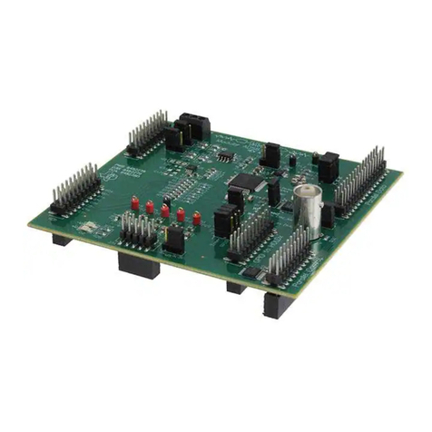
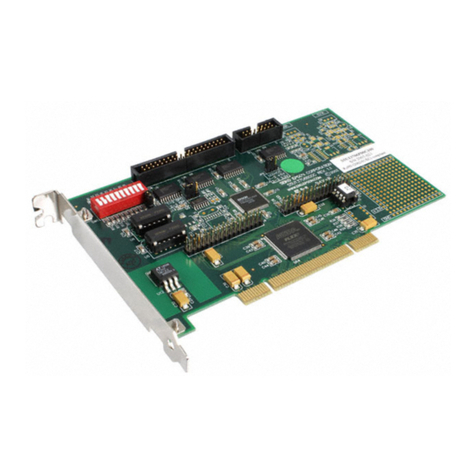
The VL supply is located at J6 on the bottom of the board and VCC is J5 located at the top of the board.
Table 3-3. Dual Supply Operation Configuration Table
Component ID Comment
J5 Connect to VL source (1.65V to 5.5V) for Logic Supply
J6 Connect to VCC Source (3V to 5.5V)
J7 Leave Open
C2, C3, C4, and/or C5 Have Minimum of 1uF of Decoupling Capacitance on VL
C6 and/or C8 If More Decoupling Capacitance is Desired Attach Capacitors to C6
and C8
R14 and/or R15 Install Resistor if Low impedance pathway between GND and
EARTH is desired
3.1.1.3 Default Operation Mode
With an understanding of how the board is setup and how to power the board for both supply situations the next
topic is how to operate the board. Out of the box the board, when powered, can operate the THVD1424 as a
full or half duplex RS-485 transceiver. The devices pins can be broken down into 4 distinct groups: single ended
communication pins, differential communication pins, power pins, and control pins. Power pins are discussed
above in the previous section, section 3.3, details below for the other 3 categories.
The single ended communication pins are to be connected directly, through their respective jumpers, to a single
ended bus – these pins are the “R” and “D” pins and represent RX and TX single ended data respectively. R is
connected to J1 and D is connected to J4 – these are the console side signal connection points for the EVM.
The THVD1424 has six control pins that vary in function. Two signals are enable signals for the driver (DE –
active high) and receiver (/RE – active low) that are accessed through J3 and J2 respectively. The other four
control signals are TERM_TX, H/F, TERM_RX, and the SLR pins which can be accessed through J8 and have
internal pull-downs leaving a default state as logic low on these four pins. A jumper configuration for J1 – J4 and
J8 are shown in Figure 3-1 with board orientation having jumper J1 at the top left corner of the board. A function
table for the control signals are shown in Table 3-4
Board Description www.ti.com
8THVD1424 Evaluation Module (EVM) User Guide SLLU356 – SEPTEMBER 2022
Submit Document Feedback
Copyright © 2022 Texas Instruments Incorporated
