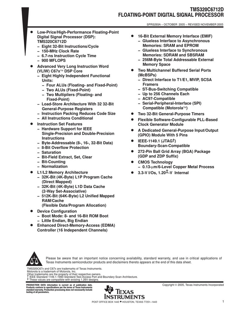
Texas Instruments TMS320C2x User manual

TMS320C2x
User's Guide
1604907-9761 revision C
January 1993

Running Title—Attribute Reference
1-1
Chapter 1
Introduction
TheTMS320familyof16/32-bitsingle-chipdigitalsignalprocessorscombines
theflexibilityofahigh-speedcontrollerwiththenumericalcapabilityofanarray
processor, offering an inexpensive alternative to custom VLSI and multichip
bit-slice processors for signal processing.
The TMS32010, the first digital signal processor in the TMS320 family, was
introduced in 1982. Since that time, the TMS320 family has established itself
astheindustrystandard for digital signalprocessing.Thepowerful instruction
set,inherentflexibility,high-speednumber-crunchingcapabilities,andinnova-
tive architecture make these high-performance, cost-effective processors
idealformanytelecommunications,computer,commercial,industrial,andmil-
itary applications.
Note:
Throughout this document, TMS320C2x refers to the TMS320C25,
TMS320C25-33, TMS320C25-50, TMS320E25, TMS320C26, and
TMS320C28 unless stated otherwise. Where applicable, ROM includes the
on-chip EPROM of the TMS320E25.
Topics in this chapter include
Topic Page
1.1 General Description 1-2. . . . . . . . . . . . . . . . . . . . . . . . . . . . . . . . . . . . . . . . . . .
1.2 Key Features 1-6. . . . . . . . . . . . . . . . . . . . . . . . . . . . . . . . . . . . . . . . . . . . . . . . .
1.3 Typical Applications 1-8. . . . . . . . . . . . . . . . . . . . . . . . . . . . . . . . . . . . . . . . . . .

General Description
1-2
Introduction
1.1 General Description
The TMS320 family currently consists of five generations: TMS320C1x,
TMS320C2x, TMS320C3x, TMS320C4x, and TMS320C5x (see Figure 1–1).
The family expansion includes enhancements of existing generations and
morepowerfulnewgenerationsofdigitalsignalprocessors.Manyfeaturesare
commonamong thesegenerations. Somespecific featuresare addedin each
processor to provide different cost/performance tradeoffs. Software compati-
bilityis maintainedthroughout thefamilytoprotecttheuser’sinvestmentinar-
chitecture. Each processor has software and hardware tools to facilitate rapid
design.
This document discusses the TMS320C2x devices:
-
TMS320C25, a CMOS 40-MHz digital signal processor capable of twice
the performance of the TMS320C1x devices
-
TMS320C25-33 a CMOS 33-MHz version of the TMS32025
-
TMS320C25-50, a CMOS enhanced-speed (50-MHz) version of the
TMS320C25
-
TMS320E25, a version of the TMS320C25 (40-MHz) with on-chip ROM
replaced by secure, on-chip EPROM
-
TMS320C26,aversionoftheTMS320C25(40-MHz)withexpandedconfi-
gurable program/data RAM
-
The TMS320C28, a version of the TMS320C25 (40-MHz) with expanded
8K-word on-chip ROM and an added power-down mode.

General Description
1-3
Figure 1–1.TMS320 Device Evolution
ÇÇ
ÇÇ
ÇÇÇÇÇÇ
ÇÇÇÇÇÇ
ÇÇÇÇÇÇ
ÇÇÇÇÇÇ
ÇÇÇÇÇÇ
ÇÇÇÇÇÇ
ÇÇÇÇÇÇ
ÇÇÇÇÇÇ
ÇÇÇÇÇÇ
ÇÇÇÇÇÇ
ÇÇÇÇÇÇ
ÇÇÇÇÇÇ
ÇÇÇÇÇÇ
ÇÇÇÇÇÇ
ÇÇÇÇÇÇ
ÇÇÇÇÇÇ
ÇÇÇÇÇÇ
ÇÇÇÇÇÇ
ÇÇÇÇÇÇ
ÇÇÇÇÇÇ
ÇÇÇÇÇÇ
ÇÇÇÇÇÇ
ÇÇÇÇÇÇ
ÇÇÇÇÇÇ
ÇÇÇÇÇÇ
ÇÇÇÇÇÇ
ÇÇÇÇÇÇ
ÇÇÇÇÇÇ
ÇÇÇÇÇÇ
ÇÇÇÇÇÇ
ÇÇÇÇÇÇ
ÇÇÇÇÇÇ
ÇÇÇÇÇÇ
ÇÇÇÇÇÇ
ÇÇÇÇÇÇ
ÇÇÇÇÇÇ
ÇÇÇÇÇÇ
ÇÇÇÇÇÇ
ÇÇÇÇÇ
ÇÇÇÇÇ
ÇÇÇÇÇ
ÇÇÇÇÇ
ÇÇÇÇÇ
ÇÇÇÇÇ
ÇÇÇÇÇ
ÇÇÇÇÇ
ÇÇÇÇÇ
ÇÇÇÇÇ
ÇÇÇÇÇ
ÇÇÇÇÇ
ÇÇÇÇÇ
ÇÇÇÇÇ
ÇÇÇÇÇ
ÇÇÇÇÇ
ÇÇÇÇÇ
ÇÇÇÇÇ
ÇÇÇÇÇ
ÇÇÇÇÇ
ÇÇÇÇÇ
ÇÇÇÇÇÇ
ÇÇÇÇÇÇ
TMS320C4x
TMS320C3x
TMS320C30
TMS320C30-27
TMS320C30-40
TMS320C31
TMS320C31-27
TMS320C31-40
TMS320C31PQA
TMS320C2x
TMS320C25
TMS320E25
TMS320C25-33
TMS320C25-50
TMS320C26
TMS320C28
TMS320C5x
TMS320C50
TMS320C51
TMS320C53
TMS320C1x
TMS320C10
TMS320C10-14/-25
TMS320C14
TMS320E14/P14
TMS320C15/LC15
TMS320E15/P15
TMS320C15-25
TMS320E15-25
TMS320C16
TMS320C17/LC17
TMS320E17/P17
Fixed-Point Generations Floating-Point Generations
TMS320C40
P
E
R
F
O
R
M
A
N
C
E
M
I
P
S
/
M
F
L
O
P
S
GENERATION
TMS320C40-40
PlansforexpansionoftheTMS320familyincludemorespinoffsoftheexisting
generations as well as more powerful future generations of digital signal pro-
cessors.
The TMS320 family combines the high performance and specialized features
necessary in digital signal processing (DSP) applications with an extensive
program of development support, including hardware and software develop-
menttools,productdocumentation,textbooks,newsletters,DSPdesignwork-
shops, and a variety of application reports. See Appendix K for a discussion
of the wide range of development tools available.

General Description
1-4
Introduction
The combination of the TMS320’s Harvard-type architecture (separate pro-
gram and data buses) and its special digital signal processing instruction set
providespeed andflexibility toexecute 12.8MIPS (millioninstructions perse-
cond). The TMS320 family optimizes speed by implementing functions in
hardware that other processors implement through software or microcode.
This hardware-intensive approach provides the design engineer with power
previously unavailable on a single chip.
The TMS320C2x generation includes six members: TMS320C25,
TMS320C25-33, TMS320C25-50, TMS320E25, TMS320C26, and
TMS320C28. Table 1–1 provides an overview of the TMS320C2x generation
of processors with comparisons of memory, I/O, cycle timing, and package
type.
Table 1–1.TMS320C2x Processors Overview
Device Memory
On-chip ROM/ Off-chip
RAM EPROM Prog Data I/O Ports †
Ser Par DMA
Cycle
Time
(ns)
Package
Type*
PGA PLCC CER QFP
TMS320C25‡ 544 4K 64K 64K Yes 16 ×16 Con 100 68 68 — —
TMS320C25-33 544 4K 64K 64K Yes 16 ×16 Con 120 —68——
TMS320C25-50§ 544 4K 64K 64K Yes 16 ×16 Con 80 —68——
TMS320E25§ 544 4K 64K 64K Yes 16 ×16 Con 100 — — 68 80
TMS320C26 1568 256 64K 64K Yes 16 ×16 Con 100 —68——
TMS320C28 544 8K 64K 64K Yes 16 ×16 Con 100 —68—80
†Ser = serial; Par = parallel; DMA = direct memory access; Con = concurrent DMA.
‡Military version available; contact nearest TI Field Sales Office for availability.
§Military version planned; contact nearest TI Field Sales Office for details.
*PGA = 68-pin grid array; PLCC = plastic-leaded chip carrier; CER = surface mount ceramic-leaded chip carrier (CER-QUAD);
QFP = plastic quad flat package
The TMS320C25, like all members of the TMS320C2x generation, is pro-
cessedin CMOS technology.TheTMS320C25iscapableofexecuting10mil-
lioninstructionspersecond. Enhanced featuressuchas24 additional instruc-
tions (133 total), eight auxiliary registers, an eight-level hardware stack, 4K
wordsofon-chipprogramROM,abit-reversedindexedaddressingmode,and
thelowpower dissipation inherent to the CMOS process contribute to the high
performance.
The TMS320C25-33 is a 33-MHz version of the TMS320C25. It is capable of
an instruction cycle of 120 ns. It is architecturally identical to the 40-MHz ver-
sionof theTMS320C25andispin-for-pinandobject-codecompatiblewith the
TMS320C25.
The TMS320C25-50 is a high-speed version of the TMS320C25. It is capable
ofaninstructioncycletimeof80ns.Itisarchitecturallyidenticaltothe40-MHz
versionof the TMS320C25 and is pin-for-pin and object-code compatible with
the TMS320C25.
General Description
1-5
The TMS320E25 is identical to the TMS320C25, except that the on-chip
4K-word program ROM is replaced with a 4K-word on-chip program EPROM.
On-chip EPROM allows realtime code development and modification for im-
mediate evaluation of system performance.
The TMS320C26 is pin-for-pin and object-code compatible (except for RAM
configurationinstructions) with the TMS320C25. Itis capableof aninstruction
cycle time of 100 ns. The enhancement over the TMS320C25 consists of a
larger, configurable, on-chip RAM divided into 4 blocks, for a total 1568-word
program/dataspace.TheTMS320C26issimilartotheTMS320C25exceptfor
its internal memory configuration. This is discussed in Section 3.4 and in Ap-
pendix B.
TheTMS320C28isobjectcode-compatiblewiththeTMS320C25.Itiscapable
ofaninstruction cycletime of 100ns. The TMS320C28contains an expanded
8K words of on-chip program ROM and an added power-down mode, which
conservespowerwhilesavingthecontentsofon-chipSRAM(B0,B1,andB2).

Key Features
1-6
Introduction
1.2 Key Features
Key features of the TMS320C2x devices are listed below. Those that pertain
to a particular device are followed by the device name within parentheses.
-
Instruction cycle timing:
80-ns (TMS320C25-50)
100-ns (TMS320C25, TMS320E25, TMS320C26, and TMS320C28)
120-ns (TMS320C25-33)
-
544-word programmable on-chip data RAM
-
1568-word configurable program/data RAM (TMS320C26 only)
-
4K-word on-chip program ROM (TMS320C25, TMS302C25-33, and
TMS320C25-50)
-
8K-word on-chip program ROM (TMS320C28 only)
-
Secure 4K-word on-chip program EPROM (TMS320E25)
-
128K-word total data/program memory space
-
32-bit ALU/accumulator
-
16- ×16-bit parallel multiplier with a 32-bit product
-
Single-cycle multiply/accumulate instructions
-
Repeat instructions for efficient use of program space and enhanced
execution
-
Block moves for data/program management
-
On-chip timer for control operations
-
Up to eight auxiliary registers with dedicated arithmetic unit
-
Up to eight-level hardware stack
-
Sixteen input and sixteen output channels
-
16-bit parallel shifter
-
Wait states for communication to slower off-chip memories/peripherals
-
Serial port for direct codec interface
-
Synchronization input for synchronous multiprocessor configurations

Key Features
1-7
-
Global data memory interface
-
TMS320C1x source-code upward compatibility
-
Concurrent DMA using an extended hold operation
-
Instructions for adaptive filtering, FFT, and extended-precision arithmetic
-
Bit-reversed indexed-addressing mode for radix-2 FFT
-
On-chip clock generator
-
Single 5-V supply
-
Power-down mode (TMS320C28 only)
-
Device packaging:
68-pin PGA (TMS320C25)
68-lead PLCC (TMS320C25, TMS320C26, and TMS320C28)
68-lead CER-QUAD (TMS320E25)
80-pin QFP (TMS320C28)
-
Commercial and military versions available

Typical Applications
1-8
Introduction
1.3 Typical Applications
TheTMS320family’suniqueversatilityandrealtimeperformanceofferflexible
design approaches in a variety of applications. In addition, TMS320 devices
cansimultaneouslyprovidethemultiplefunctionsoftenrequiredinthosecom-
plex applications. Table 1–2 lists typical TMS320 family applications.
Table 1–2.Typical Applications of the TMS320 Family
General-Purpose DSP Graphics/Imaging Instrumentation
Digital Filtering
Convolution
Correlation
Hilbert Transforms
Fast Fourier Transforms
Adaptive Filtering
Windowing
Waveform Generation
3-D Rotation
Robot Vision
Image Transmission/
Compression
Pattern Recognition
Image Enhancement
Homomorphic Processing
Workstations
Animation/Digital Map
Spectrum Analysis
Function Generation
Pattern Matching
Seismic Processing
Transient Analysis
Digital Filtering
Phase-Locked Loops
Voice/Speech Control Military
Voice Mail
Speech Vocoding
Speech Recognition
Speaker Verification
Speech Enhancement
Speech Synthesis
Text-to-Speech
Disk Control
Servo Control
Robot Control
Laser Printer Control
Engine Control
Motor Control
Secure Communications
Radar Processing
Sonar Processing
Image Processing
Navigation
Missile Guidance
Radio Frequency Modems
Telecommunications Automotive
Echo Cancellation
ADPCM Transcoders
Digital PBXs
Line Repeaters
Channel Multiplexing
1200 to 19200-bps Modems
Adaptive Equalizers
DTMF Encoding/Decoding
Data Encryption
FAX
Cellular Telephones
Speaker Phones
Digital Speech
Interpolation (DSI)
X.25 Packet Switching
Video Conferencing
Spread Spectrum
Communications
Engine Control
Vibration Analysis
Antiskid Brakes
Adaptive Ride Control
Global Positioning
Navigation
Voice Commands
Digital Radio
Cellular Telephones
Consumer Industrial Medical
Radar Detectors
Power Tools
Digital Audio/TV
Music Synthesizer
Toys and Games
Solid-State Answering
Machines
Robotics
Numeric Control
Security Access
Power Line Monitors
Hearing Aids
Patient Monitoring
Ultrasound Equipment
Diagnostic Tools
Prosthetics
Fetal Monitors
Many of the TMS320C2x features, such as single-cycle multiply/accumulate
instructions, 32-bit arithmetic unit, large auxiliary register file with a separate
arithmeticunit, and large on-chip RAM and ROM make the device particularly
applicableindigitalsignalprocessingsystems.Atthesametime,general-pur-
pose applications are greatly enhanced by the large address spaces, on-chip
timer,serialport,multipleinterruptstructure,provisionforexternalwaitstates,
and capability for multiprocessor interface and direct memory access.

Typical Applications
1-9
The TMS320C2x has the flexibility to be configured to satisfy a wide range of
systemrequirements.Thisallowsthedevicetobeappliedinsystemscurrently
using costly bit-slice processors or custom ICs. These are examples of such
system configurations:
-
A standalone system using on-chip memory,
-
Parallel multiprocessing systems with shared global data memory, or
-
Host/peripheral coprocessing using interface control signals.

1-10
Introduction

Running Title—Attribute Reference
2-1
Chapter 2
Pinouts and Signal Descriptions
The TMS320C2x generation digital signal processors are available in one or
more of four package types. The TMS320C25 (40-MHz version only) is avail-
able in a 68-pin grid array (PGA) package. The TMS320C25 (33-MHz,
40-MHz,and 50-MHzversions) andthe TMS320C26are availablein aplastic
68-lead chip carrier (PLCC) package. The TMS320E25 is packaged in a ce-
ramic surface mount 68-lead chip carrier (CER-QUAD) package. The
TMS320C28 is available in a 80-pin quad flat package (QFP). All TMS320
packages conform to JEDEC specifications.
Conversion sockets that accept PLCC and CER-QUAD packages and have
aPGA footprintare commerciallyavailable. Formore information,refer toAp-
pendix D.
Whenusing the XDSemulator, refer tosubsection 6.1.3for user targetdesign
considerations.
The TMS320C26 is similar to the TMS320C25 except for its internal memory
configuration. This is discussed in Section 3.4 and in Appendix B.
Topics in this chapter include
Topic Page
2.1 TMS320C2x Pinouts 2-2. . . . . . . . . . . . . . . . . . . . . . . . . . . . . . . . . . . . . . . . . . .
2.2 TMS320C2x Signal Descriptions 2-4. . . . . . . . . . . . . . . . . . . . . . . . . . . . . . . .

TMS320C2x Pinouts
2-2
Pinouts and Signal Descriptions
2.1 TMS320C2x Pinouts
Figure 2–1 shows pinouts of the PGA, PLCC, and CER-QUAD packages for
the TMS320C2x devices. Note that the pinout and external dimensions of
PLCC and CER-QUAD are identical. Figure 2–2 shows preliminary pinouts
of the QFP package for the TMS320C28 device.
Figure 2–1.TMS320C2x Pin Assignments
1234567891011
A
B
C
D
E
F
G
H
J
K
L
IACK
MSC
CLKOUT1
CLKOUT2
XF
HOLDA
DX
FSX
X2 CLKIN
X1
BR
D8
D9
D10
D11
D12
D13
D14
D15
READY
CLKR
CLKX
STRB
R/W
PS
IS
DS
VSS
10
11
12
13
14
15
16
17
18
19
20
21
22
23
24
25
2627 28 29 30 31 32 33 34 35 36 37 38 39 40 41 42 43
9 8 7 6 5 4 3 2 1 6867666564636261
VSS
D7
D6
D5
D4
D3
D2
D1
D0
SYNC
INT0
INT1
INT2
VCC
DR
FSR
A0
60
59
58
57
56
55
54
53
52
51
50
49
48
47
46
45
44
A1
A2
A3
A4
A5
A6
A7
A8
A9
A10
A11
A12
A13
A14
A15
VSS
VCC
VCC
VCC
68-Pin FN Plastic Leaded Chip Carrier
Package and 68-Pin FZ CER-QUAD
Package (Top View)
68-Pin GB Pin Grid Array
Ceramic Package (Top View)

†Packages are shown for pinout reference only.
CC
SS
1
2
3
4
5
6
7
8
9
10
11
12
13
14
15
16
17
18
19
20
21
22
23
24
64
63
62
61
60
59
58
57
56
55
54
53
52
51
50
49
48
47
46
45
44
43
42
41
IACK
PDI
VCC
VCC
CLKX
VSS
CLKR
RS
READY
HOLD
BIO
MP/MC
D15
VSS
D14
D13
VCC
D12
D11
D10
D0
D6
VSS
VSS
WAKEUP
VSS
A15
A14
A13
A12
VSS
A11
A10
A9
A8
VCC
VCC
A7
A6
VSS
A5
A4
A3
A2
A1
PDACK
VSS
A0
80 79 78 77 76 75 74 73 72 71 70 69 68 67 66 65
25 26 27 28 29 30 31 32 33 34 35 36 37 38 39 40
D7
D6
D5
D4
D3
D2
VD1
D0
SYNC
INT0
INT1
INT2
VDR
FSR
MSC
CLKOUT1
CLKOUT2
XF
HOLDA
V
DX
FSX
X2/CLKIN
X1
BR
STRB
R/W
PS
IS
DS
SS
80-Pin PH Quad Flat Package †
(Top View)
TMS320C2x Pinouts
2-3
Figure 2–2.TMS320C28 Pin Assignments
ADVANCE INFORMATION

TMS320C2x Signal Descriptions
2-4
Pinouts and Signal Descriptions
2.2 TMS320C2x Signal Descriptions
The signal descriptions for the TMS320C2x devices are provided in this sec-
tion. Table 2–1 lists each signal, its pin location (PGA, PLCC, and CER-
QUAD),function, andoperating mode(s): thatis, input, output,or high-imped-
ance state as indicated by I, O, or Z. The signals in Table 2–1 are grouped ac-
cording to function and alphabetized within that grouping.
Table 2–1.TMS320C2x Signal Descriptions
Signal Pin
(PGA/PLCC†)I/O/Z‡Description
Address/Data Buses
A15 MSB
A14
A13
A12
A11
A10
A9
A8
A7
A6
A5
A4
A3
A2
A1
A0 LSB
L10/43
K9/42
L9/41
K8/40
L8/39
K7/38
L7/37
K6/36
K5/34
L5/33
K4/32
L4/31
K3/30
L3/29
K2/28
K1/26
O/Z Parallel address bus A15 (MSB) through A0 (LSB).
Multiplexed to address external data/program memory or I/O.
Placed in high-impedance state in the hold mode.
D15 MSB
D14
D13
D12
D11
D10
D9
D8
D7
D6
D5
D4
D3
D2
D1
D0 LSB
B6/2
A5/3
B5/4
A4/5
B4/6
A3/7
B3/8
A2/9
B2/11
C1/12
C2/13
D1/14
D2/15
E1/16
E2/17
F1/ 18
I/O/Z Parallel data bus D15 (MSB) through D0 (LSB). Multiplexed to
transfer data between the TMS320C2x and external data/pro-
grammemoryorI/O devices.Placedin thehigh-impedancestate
when not outputting or when RS or HOLD is asserted.
Interface Control Signals
DS
PS
IS
K10/45
J10/47
J11/46
O/Z Data, program, and I/O space select signals. Always high unless
low level asserted for communicating to a particular external
space. Placed in high-impedance state in the hold mode.
READY B8/66 IDatareadyinput.Indicatesthatanexternaldeviceispreparedfor
the bus transaction to be completed. If the device is not ready
(READY = 0), the TMS320C2x waits one cycle and checks
READY again. READY also indicates a bus grant to an external
device after a BR (bus request) signal.
† Pin numbers apply to CER-QUAD as well as to PLCC.
‡ Input/Output/High-impedance state.

TMS320C2x Signal Descriptions
2-5
Table 2–1.TMS320C2x Signal Descriptions (Continued)
Signal Pin
(PGA/PLCC†)I/O/Z‡Description
Interface Control Signals (Continued)
R/W H11/48 O/Z Read/writesignal.Indicatestransferdirectionwhencommunicat-
ing to an external device. Normally in read mode (high), unless
low level asserted for performing a write operation. Placed in
high-impedance state in the hold mode.
STRB H10/49 O/Z Strobesignal. Always high unless asserted low to indicate an ex-
ternal bus cycle. Placed in high-impedance state in the hold
mode.
Multiprocessing Signals
BR G11/50 OBus request signal. Asserted when the TMS320C2x requires ac-
cess to an external global data memory space. READY is as-
sertedtothedevice whenthe busisavailable andthe globaldata
memory is available for the bus transaction.
HOLD A7/67 IHold input. When this signal is asserted, the TMS320C2x places
the data, address, and control lines in the high-impedance state.
HOLDA E10/55 OHold acknowledge signal. Indicates that the TMS320C2x has
gone into the hold mode and that an external processor may ac-
cess the local external memory of the TMS320C2x.
SYNC F2/19 ISynchronization input. Allows clock synchronization of two or
more TMS320C2xs. SYNC is an active-low signal and must be
asserted on the rising edge of CLKIN.
Interrupt and Miscellaneous Signals
BIO B7/68 IBranchcontrol input. Polled byBIOZinstruction. If BIO is low, the
TMS320C2xexecutesabranch.Thissignalmustbeactiveduring
the BIOZ instruction fetch.
IACK B11/60 OInterrupt acknowledge signal. Output is valid only while
CLKOUT1islow.Indicatesreceiptofaninterruptandthatthepro-
gram is branching to the interrupt-vector location designated by
A15–A0.
INT2
INT1
INT0
H1/22
G2/21
G1/20
IExternaluser interruptinputs. Prioritized andmaskableby the in-
terrupt mask register and the interrupt mode bit.
MP/MC A6/1 IMicroprocessor/microcomputer mode select pin for the
TMS320C25.Whenasserted low(microcomputer mode),the pin
causes the internal ROM to be mapped into the lower 4K words
of the program memory map. In the microprocessor mode, the
lower 4K words of program memory are external.
† Pin numbers apply to CER-QUAD as well as to PLCC.
‡ Input/Output/High-impedance state.

TMS320C2x Signal Descriptions
2-6
Pinouts and Signal Descriptions
Table 2–1.TMS320C2x Signal Descriptions (Continued)
Signal Pin
(PGA/PLCC†)I/O/Z‡Description
Interrupt and Miscellaneous Signals (Continued)
MSC C10/59 OMicrostate complete signal. Asserted low and valid only during
CLKOUT1 low when the TMS320C2x has just completed a
memoryoperation,suchasaninstructionfetchoradata memory
read/write. MSC can be used to generate a one wait-state
READY signal for slow memory.
RS A8/65 IResetinput. Causes the TMS320C2x toterminate execution and
forcesthe programcounter to zero.When RSis broughtto ahigh
level, execution begins at location zero of program memory. RS
affects various registers and status bits.
XF D11/56 OExternal flag output (latched software-programmable signal).
Used for signaling other processors in multiprocessor configura-
tions or as a general-purpose output pin.
Supply/Oscillator Signals
CLKOUT1 C11/58 OMasterclock output signal(CLKINfrequency/4). CLKOUT1 rises
atthe beginningofquarter-phase3(Q3)andfallsatthebeginning
of quarter-phase 1 (Q1).
CLKOUT2 D10/57 OAsecond clock output signal.CLKOUT2rises at thebeginning of
quarter-phase 2 (Q2) and falls at the beginning of quarter-phase
4 (Q4).
VCC A10/61
B10/62
H2/23
L6/35
IFour 5-V supply pins, tied together externally.
VSS B1/10
K11/44
L2/27
IThree ground pins, tied together externally.
X1 G10/51 OOutput pin from the internal oscillator for the crystal. If a crystal is
not used, this pin should be left unconnected.
X2/CLKIN F11/52 IInput pin to the internal oscillator from the crystal. If crystal is not
used, a clock may be input to the device on this pin
† Pin numbers apply to CER-QUAD as well as to PLCC.
‡ Input/Output/High-impedance state.

TMS320C2x Signal Descriptions
2-7
Table 2–1.TMS320C2x Signal Descriptions (Continued)
Signal Pin
(PGA/PLCC†)I/O/Z‡Description
Serial Port Signals
CLKR B9/64 IReceive clock input. External clock signal for clocking data from
the DR (data receive) pin into the RSR (serial port receive shift
register). Must be present during serial port transfers.
CLKX A9/63 ITransmit clock input. External clock signal for clocking data from
the XSR (serial port transmit shift register) to the DX (data trans-
mit) pin. Must be present during serial port transfers.
DR J1/24 ISerialdatareceiveinput.SerialdataisreceivedintheRSR(serial
port receive shift register) via the DR pin.
DX E11/54 O/Z Serial data transmit output. Serial data transmitted from the XSR
(serial port transmit shift register) via the DX pin. Placed in high-
impedance state when not transmitting.
FSR J2/25 IFrame synchronization pulse for receive input. The falling edge
oftheFSRpulseinitiatesthedata-receiveprocess,beginningthe
clocking of the RSR.
FSX F10/53 I/O Framesynchronizationpulsefortransmitinput/output.Thefalling
edgeof the FSXpulse initiates the data- transmitprocess,begin-
ning the clocking of the XSR. Following reset, the default operat-
ing condition of FSX is as an input. This pin may be selected by
software to be an output when the TXM bit in the status register
is set to 1.
† Pin numbers apply to CER-QUAD as well as to PLCC.
‡ Input/Output/High-impedance state.
Note: See Appendix C for TMS320C28 signal descriptions.

2-8
Pinouts and Signal Descriptions

iii
Read This First
About This Manual
The purpose of this user’s guide is to serve as a reference book for the
TMS320C2x digital signal processors. Chapters 2 through 6 provide specific
information about the architecture and operation of the devices. Appendices
A through E furnish electrical specifications and mechanical data.
How to Use This Manual
This document contains the following chapters:
Chapter 1 Introduction
Description and key features of the TMS320C2x generation of digital signal
processors.
Chapter 2 Pinouts and Signal Descriptions
Package drawings for TMS320C2x devices. Functional listings of the signals,
their pin locations, and descriptions.
Chapter 3 Architecture
TMS320C2x design description, hardware components, and device
operation. Functional block diagram and internal hardware summary table.
Chapter 4 Assembly Language Instructions
Addressing modes and format descriptions. Instruction set summary listed
according to function. Alphabetized individual instruction descriptions with
examples.
Chapter 5 Software Applications
Software application examples for the use of various TMS320C2x instruction
set features.
Chapter 6 Hardware Applications
Hardware design techniques and application examples for interfacing to
memories, peripherals, or other microcomputers/microprocessors. XDS
design considerations. System applications.
Other manuals for TMS320C2x
1
Table of contents
Other Texas Instruments Processor manuals

Texas Instruments
Texas Instruments MSP50C6xx User manual

Texas Instruments
Texas Instruments Sitara AM335x User manual

Texas Instruments
Texas Instruments OMAP5910 Product manual

Texas Instruments
Texas Instruments DM38x DaVinci User manual

Texas Instruments
Texas Instruments TMS320C6712D User manual

Texas Instruments
Texas Instruments TAS5026REF User manual

Texas Instruments
Texas Instruments Sitara AM3359 User manual

Texas Instruments
Texas Instruments TMS3320C5515 User manual

Texas Instruments
Texas Instruments TMS320DM643x User manual

Texas Instruments
Texas Instruments TMS320C6454 User manual