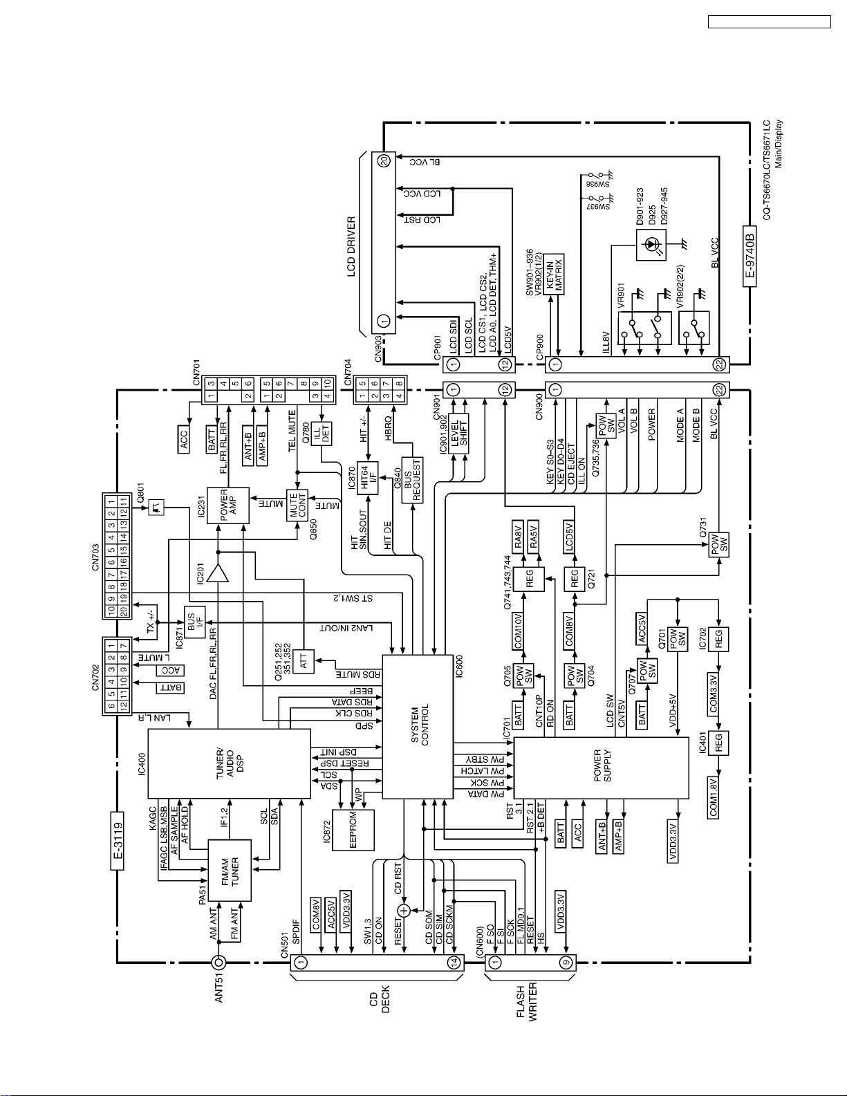
6.1. Main Block
IC600: C2DBLK000110
No. Port Descriptions I/O FM AM CD
1 AVDD Standard voltage for A/D
converter - 3.4 3.4 3.4
2 GND Ground Terminal - 0 0 0
3 ILL-DET H: Illumination off
L: Illumination on I 3.4 3.4 3.4
4 (PORT) H: LAN-MUTE off (normal)
L:LAN-MUTE on (DSP-MUTE) I 0 0 0
5 VDD - - 3.4 3.4 3.4
6 MUTE
ON/OFF H: MUTE on L: MUTE off O 0 0 0
7 NC No Connection - - - -
8 IC/
FLMD0 - - 0 0 0
9 VDDO - - 3.4 3.4 3.4
10 REGCPU Regulator output stable capacity
connection and power when
regulator stops
- 2.5 2.5 2.6
11 GND Ground - 0 0 0
12 X1 Oscillation (main clock)
4.718MHz I 1.2 1.2 1.2
13 X2 Oscillation (main clock)
4.718MHz O 1.2 1.2 1.2
14 RESET H: Normal L: Reset I 3.3 3.4 3.4
15 XT1 Oscillation (sub) 32.768kHz I - - -
16 NC No connection - - - -
17 NC No connection - - - -
18 Lo-BAT.
RESET H:+B, 3.1V or more
L: +B, less than 3.1V I 3.3 3.3 3.4
19 SW1 H: SW1 on L: SW1 off I 0 0 3.4
20 DRST On-chip debug I 0 0 0
21 PWR H: PWR off L: PWR on I 3.3 3.3 3.3
22 CD-SOM CD (IDC) deck serial
communication I 0 0 1.9
23 CD-SIM CD (IDC) deck serial
communication
H: data "1" L: data "0"
O 0 0 2.6
24 CD-
SCKM CD (IDC) deck serial
communication clock O 0 0 3.4
25 SIYOU1 Specification 1 - - - -
26 LOAD (LOAD) I 1.7 1.7 1.7
27 SW3 H: SW3 on L: SW3 off I 0 0 3.3
28 BEEP Beep output terminal O 0 0 0
29 SPD Input from the vehicle pulse
1 pulse: 1/2548km I 0 0 0
30 SIYOU2 Specification 2 - - - -
31 TX + AVC-LAN data input O 0 0 0
32 TX - AVC-LAN data output I 0 0 0
33 GND GND for I/O port and combined
function - 0 0 0
34 VDD Postive power supply for I/O port
and combined function - 3.4 3.4 3.4
35 HIT-
SOUT HIT64 data output terminal O 3.5 3.5 3.5
36 HIT SIN HIT64 data input I 4.6 4.7 4.6
37 NC No connection - - - -
38 ILL-ON H: Ill on L: Ill off O 0 0 0
39 DDI On-chip debug terminal O 0 0 0
40 DDO On-chip debug terminal O 0 0 0
41 DCK On-chip debug terminal O 0 0 0
42 DMS On-chip debug terminal O 0 0 0
43 DSP-SDA DSP (SAF7730HV) (H/L) I/O 2.7 2.7 2.7
44 DSP-SCL DSP (SAF7730HV) clock signal
output (H/L) O 2.4 2.4 2.4
45 WP H: E2PROM write protect (in)
L: E2PROM is writing (out) I/O 3.1 3.1 3.1
46 LCD-DET H: Normal L: S1D15605 sudden
drop I 4.5 4.5 4.5
47 LCD-
RESET H: Normal L: LCD reset O 4.5 4.5 4.5
48 LCD-CS2 S1D15605 chip select terminal 2 O 4.5 4.5 4.5
49 LCD-CS1 S1D15605 chip select terminal 1 O 4.5 4.5 4.5
50 LCD-A0 S1D15605 data; command
switch output O 4.5 4.5 4.5
51 LCD-
DATA S1D15605 data output/input O 0 0 0
52 LCD-SCL S1D15605 clock output O 3.4 3.4 3.4
53 RDS-
DATA RDS demodulator data input I 1.5 3.3 1.7
54 HIT-
HBRQ HIT64 BRQ terminal H: on L: off O 3.4 3.4 3.4
55 RDS-CL RDS demodulator clock input I 1.6 3.3 1.6
56 HIT-DE H: Sending data
L: Not sending data O 0 0 0
57 NC No connection - - - -
58 ACC-DET H: Acc on L: Acc off I 3.4 3.4 3.4
59 RESET_
DSP H: DSP normal L: DSP reset O 3.4 3.4 3.4
60 DSP_
INIT H: INIT complete
L: INIT incomplete I 3.3 3.3 3.3
61 +B-DET H: +B on L: +B off I 3.4 3.4 3.4
62 RDS-
MUTE H: RDSMUTE on
L: RDSMUTE off O 0 0 0
63 L/R H: Left handle L: Right handle I 3.1 3.1 3.1
64 NC No connection - - - -
65 DIV-SW H: Main is fixed L: Diver operation I 0 0 0
66 TEL-
MUTE H: VOL operation is valid
L: VOL operation is invalid I 3.4 3.4 3.4
67 CD-
RESET H: Normal L: Reset O 3.4 3.4 3.4
68 CD-ON H: CD deck microcomputer
communication is possible
L: Not possible
O 0 0 3.4
69 GND
(BVSS) (BVSS) Ground for bus interface - 0 0 0
70 VDD
(BVDD) Positive power supply for bus
interface - 3.4 3.4 3.4
71 NC No connection - - - -
72 NC No connection - - - -
73 BRIGHT-
IND - O - - -
74 NC No connection - - - -
75 CD-EJ H: CD-EJ off L: CD-EJ on I 3.3 3.3 3.3
76 FLMD1 - O 0 0 0
77 KEY-D0 Key matrix input terminal D0 I 0 0 0
78 KEY-D1 Key matrix input terminal D1 I 0 0 0
79 KEY-D2 Key matrix input terminal D2 I 0 0 0
80 KEY-D3 Key matrix input terminal D3 I 0 0 0
81 KEY-D4 Key matrix input terminal D4 I 0 0 0
82 KEY-S3 Key matrix output terminal S3 O 0 0 0
83 KEY-S2 Key matrix output terminal S2 O 0 0 0
84 PW-
STBY2 STBY2 output for power IC
(BD4902) No reversing O 3.4 3.4 3.4
85 PW-
STBY STBY output for power IC
(BD4902) No reversing O 3.4 3.4 3.4
86 PW-
LATCH Latch signal output for power IC
(BD4902) No reversing O 3.4 3.4 3.4
87 PW-SCK Clock output for power IC
(BD4902) No reversing O 0 0 0
88 PW-
DATA Data output for power IC
(BD4902) No reversing O 0 0 0
89 KEY-S1 Key matrix output terminal S1 O 0 0 0
90 KEY-S0 Key matrix output terminal S0 O 0 0 0
91 MODE-A Mode encoder input terminal A I 3.1 3.1 3.2
92 MODE-B Mode encoder input terminal B I 3.1 3.1 3.2
6 TERMINALS DESCRIPTION
6
CQ-TS6670LC / CQ-TS6671LC