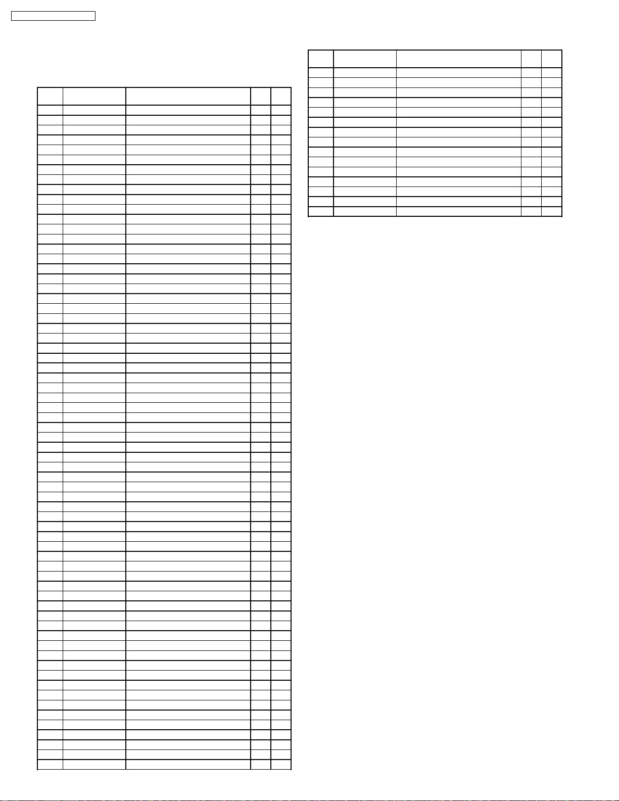
Toyota CX-WT8261A User manual

General
Power Supply DC 12V (11V - 16V),
Test Voltage 13.2V
Negative Ground
Current Consumption Less than 4A
DVD Player
Signal to Noise Ratio More than 90dB (IHF-A)
Channel Separation Less than -65dB (IHF-A)
Distortion Less than 0.05% (1kHz, 0dB)
Video Output Voltage 1.0 ± 0.2Vp-p (75Ω)
Display
Type TFT LCD
Size 7-inch wide type
CX-WT8260A
CX-WT8261A
DVD Player with Display for Rear Seat
PART No. (CX-WT8260A) : 86680-48010-A0
(CX-WT8261A) : 86680-48010-B0
VEHICLE : LEXUS
DESTINATION : North America
PRODUCED AFTER : Jan., 2003
Dimensions when closing** 306×75×323mm (W×H×D)
Weight** 2.8kg
* Specifications and the design are subject to possible modification
without notice due to improvements.
** Dimensions and Weight shown are approximate.
Specifications*
I0

1 FEATUERS 2
2 LASER PRODUCTS 2
3 SYSTEM BLOCK DIAGRAM 2
4 APPEARANCE 3
5 WIRING CONNECTION 4
6 BLOCK DIAGRAM 6
7 TERMINALS DESCRIPTION 10
8 IC BLOCK DIAGRAM 13
∙
Multi Discs Supported (DVD-V, DVD-A, V-CD, CD-DA, CD
TEXT, dtsCD, CD-R/RW).
∙
Wide Type 7-inch TFT LCD
∙
NTSC Output.
9 ADJUSTMENTS 17
10 REPLACEMENT PARTS LIST 19
11 EXPLODED VIEW (Unit) 27
12 DVD PLAYER PARTS LIST 28
13 EXPLODED VIEW (DVD Deck) 32
14 WIRING DIAGRAM 33
15 SCHEMATIC DIAGRAM 45
16 MEMO 51
∙
Tow-jack Audio Output.
∙
Wireless Audio Output.
∙
Scan, Repeat, Random function.
∙
AVC-LAN Interface.
CONTENTS
Page Page
1 FEATUERS
2 LASER PRODUCTS
3 SYSTEM BLOCK DIAGRAM
2
CX-WT8260A / CX-WT8261A

4 APPEARANCE
3
CX-WT8260A / CX-WT8261A

6 BLOCK DIAGRAM
6.1. Main, ESC, IR Block
6
CX-WT8260A / CX-WT8261A

6.2. Display Block
7
CX-WT8260A / CX-WT8261A

6.3. DVD Servo Block -1
8
CX-WT8260A / CX-WT8261A

6.4. DVD Servo Block -2
9
CX-WT8260A / CX-WT8261A

7.1. Main Block
IC600 C2CBJG000307
Pin
No. Port Descriptions I/O Vol
(V)
1 DVD RST DVD reset O 5.2
2-7 NC No connection - -
8 FLASH W_CLK Not used - -
9 FLASH W_SO Not used - -
10 FLASH W_SI Not used - -
11 RESET System reset I 5.1
12 XT2 Not used - -
13 XT1 (Connected to ground) - 0
14 VSS Ground - 0
15 X2 Crystal oscillator - 1.8
16 X1 Crystal oscillator - 1.7
17 REG OFF (Connected to ground) - 0
18 REGC Bypass capacitor terminal - 3.8
19 VDD +5V power supply - 5.2
20 B/L ADJ1 LCD backlight adjustment 1 O 0
21 B/L ADJ2 LCD backlight adjustment 2 O 0
22 B/L ADJ3 LCD backlight adjustment 3 O 0
23 B/L ADJ4 LCD backlight adjustment 4 O 5.2
24-27 B/L ADJ 11-14 Not used - -
28-30 NC No connection - -
31 KR4 Key-return detection 4 I 0
32 KR3 Key-return detection 3 I 0
33 KR2 Key-return detection 2 I 0
34 KR1 Key-return detection 1 I 0
35 KR0 Key-return detection 0 I 0
36 KS2 (COM) Key-scan 2/common O 1.8
37 KS1 Key-scan 1 O 1.8
38 KS0 Key-scan 0 O 1.9
39 NC No connection - -
40 VSS Ground - 0
41 VDD +5V power supply - 5.2
42,43 NC No connection - -
44 LOC-CNT Local control O 0
45 SW f2 Not used - -
46 L:USA H:JPN (Connected to ground) - 0
47 L:500N H:480N No connection - -
48 NC No connection - -
49 DC/DC STBY DVD power stand-by O 5.2
50 NC No connection - -
51 ILL-IND Disc indicator LED on/off O 5.2
52 NC No connection - -
53 IND Indicator LED power cont. O 5.2
54 OP/CL Open/close detection I 5.2
55 ACC.ON 5V regulator on/off O 5.2
56 ILL.ON Illumination power control O 0
57 REMO Remote control I 5.0
58 DISP-ON Display power control O 5.1
59 IR-CNT Cordless audio Tx control O 0
60 NC No connection - -
61 LAN-OFF LAN-off control O 5.2
62 NC No connection - -
63 LPF-SEL Not used - -
64 A9V-CNT ACC 9V power control O 5.2
65 NC No connection - -
66 TFT-SI TFT communication data I 4.9
67 TFT-SO TFT communication data O 5.0
68,69 NC No connection - -
70 O-MUTE Mute control O 0
71,72 NC No connection - -
73 TEST Not used - 0
74 DEG IN Temperature detection I 2.4
75-79 NC No connection - -
80 FAN-ON Fan control O 5.1
81 NC No connection - -
82 AVDD +5V power supply - 5.2
83 AVREF +5V power supply - 5.2
84 AVSS Ground - 0
Pin
No. Port Descriptions I/O Vol
(V)
85 RX Communication data I 0
86 TX Communication data O 0
87 NMI (Pulled up to VDD) - 5.1
88 /EJT Eject detection I 5.1
89 LOW+B-DET (Pulled up to VDD) - 5.1
90,91 NC (Pulled up to VDD) - 5.1
92 +B-DET Battery level detection I 5.1
93 ACC-DET ACC level detection I 5.1
94 NC No connection - -
95 DVD SO DVD serial data I 4.8
96 DVD SI DVD serial data O 5.0
97 MUTE CUT Mute enable/disable O 0
98 IEC-CNT Not used - -
99 TFT RST TFT display reset O 5.2
100 DC/DC ON TFT power control O 5.2
7 TERMINALS DESCRIPTION
10
CX-WT8260A / CX-WT8261A

7.2. DVD Servo Block
IC301 C1AB00001621
Pin
No. Port Descriptions I/O Vol
(V)
1 VDDIO I/O pad power (3.3V) - 3.3
2 MD10 SDRAM data bus I/O 0
3 MD11 SDRAM data bus I/O 0.6
4 VDD Core power (1.8V) - 1.8
5 MD12 SDRAM data bus I/O 0
6 VSSIO I/O pad ground - 0
7 MD13 SDRAM data bus I/O 0.7
8 MD14 SDRAM data bus I/O 0.5
9 MD15 SDRAM data bus I/O 0
10 VDDIO I/O pad power (3.3V) - 3.3
11 /DQM1 SDRAM data byte enable O 0
12 MA9 SDRAM address bus O 0
13 MA8 SDRAM address bus O 0
14 VSSIO I/O pad ground - 0
15 MA7 SDRAM address bus O 2.3
16 MA6 SDRAM address bus O 1.9
17 VSS Core ground - 0
18 MA5 SDRAM address bus O 1.1
19 VDDIO I/O pad power (3.3V) - 3.3
20 MA4 SDRAM address bus O 2.0
21 MA3 SDRAM address bus O 2.3
22 MCLK SDRAM clock O 1.7
23 VSSIO I/O pad ground - 0
24 CKE SDRAM clock enable O 3.3
25 MA2 SDRAM address bus O 2.3
26 MA1 SDRAM address bus O 1.0
27 VDDIO I/O pad power (3.3V) - 3.3
28 MA0 SDRAM address bus O 1.0
29 MA10 SDRAM address bus O 0
30 MA11 Not used - -
31 VSSIO I/O pad ground - 0
32 MA12 SDRAM address bus O 2.1
33 MA13 SDRAM address bus O 2.1
34 VDD Core power (1.8V) - 1.8
35 /CS0 SDRAM primary bank chip
select O 2.7
36 VDDIO I/O pad power (3.3V) - 3.3
37 /RAS SDRAM row address select O 3.1
38 /CAS SDRAM column address select O 2.9
39 /WE SDRAM write enable O 3.2
40 VSSIO I/O pad ground - 0
41 /DQM0 SDRAM data byte enable O 0
42 /DQM2 SDRAM data byte enable O 0
43 MD16 SDRAM data bus I/O 0.5
44 VDDIO I/O pad power (3.3V) - 3.3
45 MD17 SDRAM data bus I/O 0.5
46 MD18 SDRAM data bus I/O 0.5
47 VSS Core ground - 0
48 MD19 SDRAM data bus I/O 0.7
49 VSSIO I/O pad ground - 0
50 MD20 SDRAM data bus I/O 0
51 MD21 SDRAM data bus I/O 1.5
52 MD22 SDRAM data bus I/O 1.0
53 VDDIO I/O pad power (3.3V) - 3.3
54 MD23 SDRAM data bus I/O 0
55 MD24 SDRAM data bus I/O 0.5
56 MD25 SDRAM data bus I/O 0.5
57 VSSIO I/O pad ground - 0
58 MD26 SDRAM data bus I/O 0.5
59 MD27 SDRAM data bus I/O 0.8
60 MD28 SDRAM data bus I/O 0
61 MD29 SDRAM data bus I/O 1.0
62 VDDIO I/O pad power (3.3V) - 3.3
63 MD30 SDRAM data bus I/O 0.7
64 MD31 SDRAM data bus I/O 0.5
65 /DQM3 SDRAM data byte enable O 0
66 /CS1 Not used O -
67 VSSIO I/O pad ground - 0
68 SPDIF S/PDIF digital audio output O 1.3
69 VSS Core ground - 0
Pin
No. Port Descriptions I/O Vol
(V)
70 AIN Digital audio input I 3.3
71 AOUT3 Serial audio data
(Left/Right) O 0
72 AOUT2 Serial audio data
(Center/LFE) O 0
73 AOUT1 Serial audio data (Sound
Left/Right) O 0
74 AOUT0 Serial audio data
(Left/Right) O 0
75 VDDIO I/O pad power (3.3V) - 3.3
76 PCMCLK Audio DAC PCM sampling
clock O 1.8
77 VDD Core power (1.8V) - 1.8
78 ACLK Audio interface serial data
clock O 1.7
79 LRCLK Left/Right channel clock O 1.7
80 /SRST Reset signal O 3.3
81 /RSTP Power on reset I 3.3
82 VSSIO I/O pad ground - 0
83 RXD1 Not used - -
84 SSPIN1 SSP1 data in / UART1 16-
time clock I/O 1.5
85 VSS Core ground - 0
86 SSPOUT1 SSP1 data out / UART1 DTR I/O 0
87 SSPCLK1 SSP1 clock / UART1 CTS I/O 3.3
88 SSPCLK0 Not used - -
89 VDD Core power (1.8V) - 1.8
90 SSIN0 Not used - -
91 VDDIO I/O pad power (3.3V) - 3.3
92 SSPOUT0 Not used - -
93 TXD0 UART0 serial data O 3.2
94 RXD0 UART0 serial data I 3.0
95 /CTS0 Not used - -
96 /RTS0 YART0 RTS O 0
97 VSSIO I/O pad ground - 0
98 CXI Crystal Oscillator terminal I 1.6
99 CXO Not used - -
100 OSCVSS Oscillator ground - 0
101 OSCVDD Oscillator power (1.8V) - 1.8
102 MVCLVDD Main/Video clock-PLL power
(3.3V) - 3.3
103 SCEN Not used - -
104 MVCKVSS Main/Video clock-PLL Ground - 0
105 ACLKVSS Audio clock-PLL ground - 0
106 SCMD Not used - -
107 ACLKVDD Audio clock PLL power - 3.3
108 VDDDAC DAC digital power (1.8V) - 1.8
109 VSSDAC DAC digital ground - 0
110 CVBS2/CR/R Pulled down to ground O 0
111 IOM Pulled down to ground O 0
112 C/CB/B Pulled down to ground O 0
113 VAA3 DAC analog power (3.3V) - 3.3
114 Y/G Pulled down to ground O 0.4
115 VSSA DAC analog ground - 0
116 VREF Not used - -
117 VAA Pulled down to ground - 1.8
118 CVBS/C Composite/S-Video
Chrominance O 0.5
119 RSET Current setting resistor
terminal O 1.4
120 COMP Compensation capacitor
terminal O 2.0
121 VSS Core ground - 0
122 VCLK Not used - -
123 VSYNC Not used - -
124 HSYNC Not used - -
125 VDDIO I/O pad power (3.3V) - 3.4
126-
131 VI07-02 Not used - -
132 VSSIO I/O pad ground - 0
133 Not used - - -
134 Not used - - -
135 VDD Core power (1.8V) - 1.9
136-
139 AD31-28 Not used - -
140 VDDIO I/O pad power (3.3V) - 3.4
11
CX-WT8260A / CX-WT8261A

Pin
No. Port Descriptions I/O Vol
(V)
141-
144 AD27-24 Not used - -
145 /PWE3 Not used - -
146 AD23 Not used - -
147 VSSIO I/O pad ground - 0
148-
150 AD22-20 Not used - -
151-
153 AD19-17 Address/Data bus I/O 0
154 VDDIO I/O pad power (3.3V) - 3.4
155 AD16 Address/Data bus I/O 0
156 /PWE2 Not used - -
157,
158 AD15, 14 Address/Data bus I/O 0
159 VDD Core power (1.8V) - 1.9
160 SCLK External bus clock O 2.1
161 ACK WAIT/ACK/RDY control I 3.4
162 VSSIO I/O pad ground - 0
163-
168 AD13-08 Address/Data bus I/O 0
169 VDDIO I/O pad power (3.3V) - 3.4
170 /PWE1 Not used - -
171 VSS Core ground - 0
172-
176 AD7-3 Address/Data bus I/O 0
177 VSSIO I/O pad ground - 0
178-
180 AD02-00 Address/Data bus I/O 0
181 VDDIO I/O pad power (3.3V) - 3.4
182 /PWE0 Byte write enable O 0
183 ALE Address latch enable O 0
184-
187 LA0-3 Latch address O 3.3
188 VSSIO I/O pad ground - 0
189 RD Read signal O 3.4
190 LHLDA Not used - -
191 LHLD Not used - -
192 VDD Core power (1.8V) - 1.9
193 /PCS0 Peripheral LSI chip select
0O 3.4
194 XI01 Not used - -
195 DACCS2 DAC output select 2 O 3.4
196 VDDIO I/O pad power (3.3V) - 3.4
197 DACCS1 DAC output select 1 O 3.4
198 NINTCPPM CPPM interrupt I 0
199 CPPMCS CPPM LSI chip select O 3.4
200 XI06 Not used - -
201 VSS Core ground - 0
202 FRAMCS FRAM chip select O 0
203 ASEL Audio selection O 0
204 VSSIO I/O pad ground - 3.4
205 FEPCS Front End Pro. LSI chip
select O 3.4
206 FEPRST Front End Pro. reset O 3.4
207 SODCCS SODC LSI chip select O 3.4
208 NINTHOST HOST interrupt I 3.4
209 NINTDDC DDC interrupt I 3.2
210 VDDIO I/O pad power (3.3V) - 3.4
211 NINTDSC DSC interrupt I 3.5
212 VDD Core power (1.8V) - 1.9
213 DSYNV DVD parallel SYNC I 3.4
214 DREQ DVD parallel data request O 3.4
215 DCLK Data sampling clock I 3.4
216 DSTB Parallel data valid/Serial
clock I 0.7
217 DVD0 DVD drive parallel data I 0
218 VSSIO I/O pad ground - 0
219 DVD1 DVD drive parallel data I 0
220 DVD2 DVD drive parallel data I 0
221 DVD3 DVD drive parallel data I 3.4
222 DVD4 DVD drive parallel data I 0.8
223 DVD5 DVD drive parallel data I 0.8
224 VDDIO I/O pad power (3.3V) - 3.4
225 DVD6 DVD drive parallel data I 3.4
226 DVD7 DVD drive parallel data I 3.4
Pin
No. Port Descriptions I/O Vol
(V)
227 MD0 SDRAM data bus I/O 0.5
228 VSSIO I/O pad ground - 0
229 MD1 SDRAM data bus I/O 0
230 VSS Core ground - 0
231 MD2 SDRAM data bus I/O 0.8
232 MD3 SDRAM data bus I/O 0.8
233 VDDIO I/O pad power (3.3V) - 3.3
234 MD4 SDRAM data bus I/O 3.3
235 MD5 SDRAM data bus I/O 0
236 MD6 SDRAM data bus I/O 0.8
237 VSSIO I/O pad ground - 0
238 MD7 SDRAM data bus I/O 0
239 MD8 SDRAM data bus I/O 0
240 MD9 SDRAM data bus I/O 0
12
CX-WT8260A / CX-WT8261A

8.1. Main Block
IC200 : C0ABCB000030
IC201 : C0JBAS000146
IC601 : C1EB00000001
IC603 : YEAMT7ST32UL
IC670 : AN31910A-NF
IC751 : C0CBCBG00002
IC950 : C1AB00000003
8 IC BLOCK DIAGRAM
13
CX-WT8260A / CX-WT8261A

8.2. Display Block
IC551 : AN8049SH-E1
IC601 : C3EBDC000049
IC801 : C0EBH0000058
14
CX-WT8260A / CX-WT8261A

IC202 : MN13821JP
IC203, 204 : YEAMT7ST08UL
IC206, 207 : C0JBAZ001014
IC305, 306 : C0JBAH000082
IC501 : C3GBCC000001
8.3. IR Block
IC401 : C0ABBB000179
8.4. DVD Servo Block
15
CX-WT8260A / CX-WT8261A

IC502 : C0JBAB000255
IC602 : C0JBAR000191
IC703 : C0JBAB000175
IC307 : C3ABPJ000028
16
CX-WT8260A / CX-WT8261A

9.1. Flicker Adjustment
<Preparation>
*1: Refer to ´SYSTM BLOCK DIAGRAM´.
*2: The following things can generate horizontal bars:
∙
AVN with Video output
∙
Pattern generator and so on.
<View Angle>
<Adjustment point>
∙
VR801 on the Display PCB
1.Turn the power on and enter to the video mode.
2.Adjust VR801 so that the flicker becomes minimum.
3.Turn the power off to finish the adjustment.
9.2. PD Pulse Width Adjustment
<Preparation>
∙
Oscilloscope
<Test Point>
∙
PD test point of the same line as IC802 pin33
<Adjustment Point>
∙
R829 (Variable resistor) on the Display PCB
<Adjustment Procedure>
1.Monitor the waveform at the test point by oscilloscope.
2.Adjust R829 so that the pulse width satisfies the following
condition.
T = 3.2µs ±0.1µs
9 ADJUSTMENTS
17
CX-WT8260A / CX-WT8261A

9.3. Carrier Frequency Adjustment
In this adjustment, two frequencies, which are for audio L-ch (2.3MHz) and R-ch (2.8MHz) signals on the IR PCB, can be set to the
target frequencies by using the variable resistors (VR400 and VR450).
You should pick up the L/R mixed signal on the IR PCB and separate them by the BPF, and then set to each frequency.
<Preparation>
∙
Dedicated Tool
∙
Frequency Counter
∙
Power Supply (9V)
<Adjustment Point>
∙
VR450 on the IR PCB for L-ch
∙
VR400 on the IR PCB for R-ch
<Target Frequency>
∙
L-ch (VR450): 2305 ±5 kHz
∙
R-ch (VR400): 2805 ±5 kHz
<Adjustment Procedure>
1.Insert the connector of dedicated tool to CN450.
2.Turn the power on.
3.Change the L/R switch to L-ch side.
4.Adjust VR450 (L-ch) for the target frequency while confirming it by the frequency counter.
5.Change the L/R switch to R-ch side.
6.Adjust VR400 (R-ch) for the target frequency while confirming it by the frequency counter.
7.Turn the power off and remove the connector to finish the adjustment.
18
CX-WT8260A / CX-WT8261A

10 REPLACEMENT PARTS
LIST
Notes :
1.Be sure to make your orders of replacement parts
according to this list.
2.Important safety notice: Components, identified by mark
have special characteristics important for safety. When
replacing any of these components, use only
manufacturer´s specified parts.
3.Location keys in the remarks column indicates the general
location of the parts shown in the exploded drawing, as in a
road map.
4.The marking (RTL) indicates that Retention Time is limited
for this item. After the discontinuation of assembly in
production, the item will continue to be available for a
specific period of time. The retention period of availability is
dependent on the type of assembly, and in accordance with
the laws governing part and product retention. After the end
of this period, the assembly will no longer be available.
5. "A" or "B" marks in remarks column are indicated as
follows :
∙
A : CX-WT8260A
∙
B : CX-WT8261A
Ref.
No. Part No. Part Name & Description Remarks
[E9164A] Main Block
IC´s and TRANSISTORs
IC200 C0ABCB000030 IC
IC201 C0JBAS000146 IC
IC600 C2CBJG000307 IC
IC601 C1EB00000001 IC
IC603 YEAMT7ST32UL IC
IC670 AN31910A-NF IC
IC700 C0CBADE00034 IC
IC702 C0DAEZH00007 IC
IC703 C0CAZHG00001 IC
IC704 YEAMA41W12ST IC
IC705 YEAMPQ30RV2 IC
IC750 C0DBAZZ00012 IC
IC751 C0CBCBG00002 IC
IC950 C1AB00000003 IC
Q602 YEANC114YKX Transistor
Q603 B1GDCFNN0002 Transistor
Q605 B1GDCFJJ0002 Transistor
Q606 YEANC1621T2 Transistor
Q700 B1BBAC000007 Transistor
Q702 YEANHQ1F3PT1 Transistor
Q703 B1GBCFNN0004 Transistor
Q704 B1GDCFNN0002 Transistor
Q705 B1GBCFNL0001 Transistor
Q706 2SB1398QTA Transistor
Q707 YEANC114YKX Transistor
Q710 YEANFP1F3PT1 Transistor
Q711 YEANC114YKX Transistor
Q712 YEANFP1F3PT1 Transistor
Q713 YEANC114YKX Transistor
Q715 B1GDCFJN0004 Transistor
Q716 B1GBCFNN0004 Transistor
Q731 B1GBCFJJ0007 Transistor
Q732 B1GBCFJJ0007 Transistor
Q733 B1GBCFJJ0007 Transistor
Q734 B1GBCFJJ0007 Transistor
Q750 YEAN2SA1244L Transistor
Q751 YEAN2SA1244L Transistor
Q752 YEANC114YKX Transistor
Ref.
No. Part No. Part Name & Description Remarks
DIODEs
D600 YEADRD18M2T1 Diode
D601 YEADRD18M2T1 Diode
D604 MA152WKTX Diode
D700 B0BC02700005 Diode
D701 MAZ81800ML Diode
D702 YEADSR1544TL Diode
D704 YEADRB051L40 Diode
D706 YEADRB051L40 Diode
D707 YEADRB051L40 Diode
D710 YEADSR1544TL Diode
D750 YEADRB051L40 Diode
D751 YEADRB051L40 Diode
D795 B0ACCK000005 Diode
D920 B0BC5R700005 Diode
D952 B0BD6R800002 Diode
CAPACITORs
C200 ECEA1CPK100I Electrolytic, 10µF 16WV
C201 ECEA1CPK100I Electrolytic, 10µF 16WV
C202 YECUZ1H332KX Ceramic, 3300PF 50WV
C203 F1J1H102A422 Ceramic, 1000PF 50WV
C204 F1J1H102A422 Ceramic, 1000PF 50WV
C205 F1H1H470A231 Ceramic, 47PF 50WV
C206 ECEA1CPD100I Electrolytic, 10µF 16WV
C207 ECEA1CPD100I Electrolytic, 10µF 16WV
C220 F1J2A101A003 Ceramic, 100PF 100WV
C221 F1J2A101A003 Ceramic, 100PF 100WV
C222 F1J2A101A003 Ceramic, 100PF 100WV
C223 F1J2A101A003 Ceramic, 100PF 100WV
C224 F1J2A101A003 Ceramic, 100PF 100WV
C225 F1J2A101A003 Ceramic, 100PF 100WV
C300 ECEA1CPK100I Electrolytic, 10µF 16WV
C301 ECEA1CPK100I Electrolytic, 10µF 16WV
C302 YECUZ1H332KX Ceramic, 3300PF 50WV
C303 F1J1H102A422 Ceramic, 1000PF 50WV
C304 F1J1H102A422 Ceramic, 1000PF 50WV
C305 F1H1H470A231 Ceramic, 47PF 50WV
C306 ECEA1CPD100I Electrolytic, 10µF 16WV
C307 ECEA1CPD100I Electrolytic, 10µF 16WV
C320 F1J2A101A003 Ceramic, 100PF 100WV
C321 F1J2A101A003 Ceramic, 100PF 100WV
C322 F1J2A101A003 Ceramic, 100PF 100WV
C323 F1J2A101A003 Ceramic, 100PF 100WV
C324 F1J2A101A003 Ceramic, 100PF 100WV
C325 F1J2A101A003 Ceramic, 100PF 100WV
C600 F1J1H1020024 Ceramic, 1000PF 50WV
C601 F1H1H180A231 Ceramic, 18PF 50WV
C602 F1H1H180A231 Ceramic, 18PF 50WV
C603 F1J1H221A672 Ceramic, 220PF 50WV
C604 F1J1H221A672 Ceramic, 220PF 50WV
C605 F1J1H221A672 Ceramic, 220PF 50WV
C606 YECUZ1H102KX Ceramic, 1000PF 50WV
C608 YECUS1C104KX Ceramic, 0.1µF 16WV
C609 YECUZ1H102KX Ceramic, 1000PF 50WV
C611 F1J1H1020024 Ceramic, 1000PF 50WV
C637 F1H1H101A231 Ceramic, 100PF 50WV
C638 F1H1H101A231 Ceramic, 100PF 50WV
C639 F1H1H101A231 Ceramic, 100PF 50WV
C640 F1H1H101A231 Ceramic, 100PF 50WV
C641 F1J1H101A672 Ceramic, 100PF 50WV
C670 YECUZ1E223KX Ceramic, 0.022µF 25WV
C672 YECUZ1C104KX Ceramic, 0.1µF 16WV
C673 YECUZ1C104KX Ceramic, 0.1µF 16WV
C700 F1J1E2240009 Ceramic, 0.22µF 25WV
C701 F1J1E2240009 Ceramic, 0.22µF 25WV
C702 ECA1CDT222U Electrolytic, 2200µF 16WV
C703 YECUZ1H103KX Ceramic, 0.01µF 50WV
C704 EEVHA1E220P Electrolytic, 22µF 25WV
C705 F2G0J2210002 Electrolytic, 220µF 6.3WV
C706 YECUZ1C104KX Ceramic, 0.1µF 16WV
19
CX-WT8260A / CX-WT8261A

Ref.
No. Part No. Part Name & Description Remarks
C708 F1J1C1050013 Ceramic, 1µF 16WV
C709 YECUS1C104KX Ceramic, 0.1µF 16WV
C710 YECUZ1C104KX Ceramic, 0.1µF 16WV
C711 YECUZ1C104KX Ceramic, 0.1µF 16WV
C712 YECUS1C104KX Ceramic, 0.1µF 16WV
C713 YECUZ1C104KX Ceramic, 0.1µF 16WV
C714 F2G0J2210002 Electrolytic, 220µF 6.3WV
C715 EEVHA0J470R Electrolytic, 47µF 6.3WV
C716 EEVHA0J470R Electrolytic, 47µF 6.3WV
C717 YECUZ1C104KX Ceramic, 0.1µF 16WV
C718 ECEA1CPD100I Electrolytic, 10µF 16WV
C719 ECA1CHG331B Electrolytic, 330µF 16WV
C720 YECUS1C104KX Ceramic, 0.1µF 16WV
C721 YECUS1C104KX Ceramic, 0.1µF 16WV
C722 EEUFC1C820H Electrolytic, 82µF 16WV
C723 YECUZ1C104KX Ceramic, 0.1µF 16WV
C724 ECEA1CPD220I Electrolytic, 22µF 16WV
C727 ECEA1APD470I Electrolytic, 47µF 10WV
C729 YECUZ1C104KX Ceramic, 0.1µF 16WV
C731 ECEA1APD470I Electrolytic, 47µF 10WV
C732 YECUS1C104KX Ceramic, 0.1µF 16WV
C733 ECA1CHG331B Electrolytic, 330µF 16WV
C734 EEUFC1C820H Electrolytic, 82µF 16WV
C735 YECUZ1H103KX Ceramic, 0.01µF 50WV
C736 EEVHA0J101P Electrolytic, 100µF 6.3WV
C737 ECA1CHG331B Electrolytic, 330µF 16WV
C738 YECUS1C104KX Ceramic, 0.1µF 16WV
C740 EEUFC1C820H Electrolytic, 82µF 16WV
C741 YECUS1C104KX Ceramic, 0.1µF 16WV
C742 ECA1CHG331B Electrolytic, 330µF 16WV
C743 EEUFC1C820H Electrolytic, 82µF 16WV
C744 YECUS1C104KX Ceramic, 0.1µF 16WV
C745 EEUFC1C820H Electrolytic, 82µF 16WV
C746 YECUS1C104KX Ceramic, 0.1µF 16WV
C747 F1J1E2240009 Ceramic, 0.22µF 25WV
C748 F1J1E2240009 Ceramic, 0.22µF 25WV
C749 EEVHA1C100R Electrolytic, 10µF 16WV
C750 EEVFC1E330P Electrolytic, 33µF 25WV
C751 EEVFC1E330P Electrolytic, 33µF 25WV
C752 YECUZ1H102KX Ceramic, 1000PF 50WV
C753 YECUZ1H102KX Ceramic, 1000PF 50WV
C754 YECUZ1H102KX Ceramic, 1000PF 50WV
C756 YECUZ1H103KX Ceramic, 0.01µF 50WV
C757 YECUZ1H102KX Ceramic, 1000PF 50WV
C758 EEVFC1E330P Electrolytic, 33µF 25WV
C759 YECUZ1H103KX Ceramic, 0.01µF 50WV
C760 EEVFC1C100R Electrolytic, 10µF 16WV
C761 YECUZ1H271JC Ceramic, 270PF 50WV
C763 YECUZ1H102KX Ceramic, 1000PF 50WV
C764 YECUZ1H102KX Ceramic, 1000PF 50WV
C765 EEVFC1E330P Electrolytic, 33µF 25WV
C766 EEVFC1E330P Electrolytic, 33µF 25WV
C767 EEVFC1E330P Electrolytic, 33µF 25WV
C768 EEVFC1E330P Electrolytic, 33µF 25WV
C769 EEVFC1E330P Electrolytic, 33µF 25WV
C770 EEVFC0J101P Electrolytic, 100µF 6.3WV
C771 EEFCD1B220R Electrolytic, 22µF 12.5WV
C772 YECUZ1H103KX Ceramic, 0.01µF 50WV
C773 EEFCD1B220R Electrolytic, 22µF 12.5WV
C774 EEVHA0J101P Electrolytic, 100µF 6.3WV
C775 EEVFC0J101P Electrolytic, 100µF 6.3WV
C776 EEFCD0J470R Electrolytic, 47µF 6.3WV
C777 YECUZ1H103KX Ceramic, 0.01µF 50WV
C778 EEFCD0J470R Electrolytic, 47µF 6.3WV
C779 EEVHA0J101P lectrolytic, 100µF 6.3WV
C780 EEVFC0J470R Electrolytic, 47µF 6.3WV
C781 F1H1H101A231 Ceramic, 100PF 50WV
C782 F1J1H101A672 Ceramic, 100PF 50WV
C783 F1J1H101A672 Ceramic, 100PF 50WV
C784 F1H1H101A231 Ceramic, 100PF 50WV
C785 YECUZ1C104KX Ceramic, 0.1µF 16WV
C786 F1J1H1020024 Ceramic, 1000PF 50WV
C787 YECUZ1H102KX Ceramic, 1000PF 50WV
Ref.
No. Part No. Part Name & Description Remarks
C788 YECUZ1H102KX Ceramic, 1000PF 50WV
C789 YECUZ1H102KX Ceramic, 1000PF 50WV
C790 YECUZ1H102KX Ceramic, 1000PF 50WV
C791 F1H1H101A231 Ceramic, 100PF 50WV
C795 YECUS1C104KX Ceramic, 0.1µF 16WV
C920 YECUS1H390JM Ceramic, 39PF 50WV
C921 F1H1H390A230 Ceramic, 39PF 50WV
C922 F1H1H390A230 Ceramic, 39PF 50WV
C923 F1H1H390A230 Ceramic, 39PF 50WV
C924 F1H1H390A230 Ceramic, 39PF 50WV
C926 F1J1H101A672 Ceramic, 100PF 50WV
C951 YECUZ1C104KX Ceramic, 0.1µF 16WV
C952 YECUZ1C104KX Ceramic, 0.1µF 16WV
C953 YECUZ1C104KX Ceramic, 0.1µF 16WV
C955 YECUZ1C104KX Ceramic, 0.1µF 16WV
C956 F1J0J4750001 Ceramic, 4.7µF 6.3WV
C957 ECEA0JKS331I Electrolytic, 330µF 6.3WV
J702 YECUS1C104KX Ceramic, 0.1µF 16WV
RESISTORs
FB200 ERJ3GEY0R00V Chip, 0Ω
ΩΩ
Ω1/16W
FB201 ERJ3GEY0R00V Chip, 0Ω
ΩΩ
Ω1/16W
FB300 ERJ3GEY0R00V Chip, 0Ω
ΩΩ
Ω1/16W
FB301 ERJ3GEY0R00V Chip, 0Ω
ΩΩ
Ω1/16W
FB721 ERJ6GEY0R00V Chip, 0Ω
ΩΩ
Ω1/10W
FB761 ERJ8GEY0R00V Chip, 0Ω
ΩΩ
Ω1/8W
J600 ERJ3GEY0R00V Chip, 0Ω
ΩΩ
Ω1/16W
J605 ERJ3GEY0R00V Chip, 0Ω
ΩΩ
Ω1/16W
J606 ERJ3GEY0R00V Chip, 0Ω
ΩΩ
Ω1/16W
J607 ERJ3GEY0R00V Chip, 0Ω
ΩΩ
Ω1/16W
J608 ERJ3GEY0R00V Chip, 0Ω
ΩΩ
Ω1/16W
J611 ERJ3GEY0R00V Chip, 0Ω
ΩΩ
Ω1/16W
J612 ERJ3GEY0R00V Chip, 0Ω
ΩΩ
Ω1/16W
J613 ERJ3GEY0R00V Chip, 0Ω
ΩΩ
Ω1/16W
J620 ERJ3GEYJ471V Chip, 470Ω
ΩΩ
Ω1/16W
J621 ERJ3GEYJ471V Chip, 470Ω
ΩΩ
Ω1/16W
J622 ERJ3GEYJ471V Chip, 470Ω
ΩΩ
Ω1/16W
J623 ERJ3GEYJ471V Chip, 470Ω
ΩΩ
Ω1/16W
J631 ERJ6GEY0R00V Chip, 0Ω
ΩΩ
Ω1/10W
J645 ERJ6GEYJ104 Chip, 100kΩ
ΩΩ
Ω1/10W
J666 ERJ6GEY0R00V Chip, 0Ω
ΩΩ
Ω1/10W
J700 ERJ6GEY0R00V Chip, 0Ω
ΩΩ
Ω1/10W
J701 ERJ6GEY0R00V Chip, 0Ω
ΩΩ
Ω1/10W
J704 ERJ6GEY0R00V Chip, 0Ω
ΩΩ
Ω1/10W
J710 ERJ6GEY0R00V Chip, 0Ω
ΩΩ
Ω1/10W
J713 ERJ6GEY0R00V Chip, 0Ω
ΩΩ
Ω1/10W
J714 ERJ6GEY0R00V Chip, 0Ω
ΩΩ
Ω1/10W
J715 ERJ6GEY0R00V Chip, 0Ω
ΩΩ
Ω1/10W
J718 ERJ6GEY0R00V Chip, 0Ω
ΩΩ
Ω1/10W
J719 ERJ6GEY0R00V Chip, 0Ω
ΩΩ
Ω1/10W
J720 ERJ6GEY0R00V Chip, 0Ω
ΩΩ
Ω1/10W
J725 ERJ6GEY0R00V Chip, 0Ω
ΩΩ
Ω1/10W
J726 ERJ6GEY0R00V Chip, 0Ω
ΩΩ
Ω1/10W
J728 ERJ6GEY0R00V Chip, 0Ω
ΩΩ
Ω1/10W
J730 ERJ6GEY0R00V Chip, 0Ω
ΩΩ
Ω1/10W
J735 ERJ12Y0R00H Chip, 0Ω
ΩΩ
Ω1/2W
J740 ERJ6GEY0R00V Chip, 0Ω
ΩΩ
Ω1/10W
J750 ERJ6GEY0R00V Chip, 0Ω
ΩΩ
Ω1/10W
J752 ERJ6GEY0R00V Chip, 0Ω
ΩΩ
Ω1/10W
J795 ERJ6GEY0R00V Chip, 0Ω
ΩΩ
Ω1/10W
J903 ERJ6GEY0R00V Chip, 0Ω
ΩΩ
Ω1/10W
J910 ERJ3GEY0R00V Chip, 0Ω
ΩΩ
Ω1/16W
J915 ERJ3GEY0R00V Chip, 0Ω
ΩΩ
Ω1/16W
J916 ERJ3GEY0R00V Chip, 0Ω
ΩΩ
Ω1/16W
J917 ERJ3GEY0R00V Chip, 0Ω
ΩΩ
Ω1/16W
R202 ERJ3GEYJ392V Chip, 3.9kΩ
ΩΩ
Ω1/16W
R203 ERJ3GEYJ392V Chip, 3.9kΩ
ΩΩ
Ω1/16W
R204 ERJ3GEYJ202V Chip, 2kΩ
ΩΩ
Ω1/16W
R205 ERJ3GEYJ202V Chip, 2kΩ
ΩΩ
Ω1/16W
R206 ERJ3GEYJ201V Chip, 200Ω
ΩΩ
Ω1/16W
R207 ERJ3GEYJ201V Chip, 200Ω
ΩΩ
Ω1/16W
R208 ERJ3GEYJ103V Chip, 10kΩ
ΩΩ
Ω1/16W
20
CX-WT8260A / CX-WT8261A
This manual suits for next models
1
Table of contents
Other Toyota Car Stereo System manuals

Toyota
Toyota 08601-00911 User manual

Toyota
Toyota Audio 2000 Avensis User manual

Toyota
Toyota 08601-00911 User manual

Toyota
Toyota 08691-00834 User manual

Toyota
Toyota PT296-00170 User manual

Toyota
Toyota CQ-TS7421K User manual

Toyota
Toyota TAS200 User manual

Toyota
Toyota TAS500 User manual

Toyota
Toyota CQ-ES0470K User manual

Toyota
Toyota CQ-TS6670LC User manual