Twiga TV10 0071 User manual

Technical manual – LVDS to YPbPr, CVBS converter board 1/9
Technical manual
LVDS to YPbPr, CVBS
converter board
TV10 0071
Ref: LVDS_YPbPr_SD_Technical_Manual
Date: 10 Jan 2020

Technical manual – LVDS to YPbPr, CVBS converter board 2/9
Documentation Revision History
Date
Revision
Description
Modified by
Note
10/01/20
B
In Specification: Modification of video formats
for SD and HD analogue outputs
NMA
Contents
Product overview ......................................................................................................................................3
Synoptics ..............................................................................................................................................3
1 Main function ...............................................................................................................................3
Specifications .......................................................................................................................................3
2 LVDS camera input ......................................................................................................................3
3 SD Analog Outputs.......................................................................................................................3
4 HD Analog Outputs ......................................................................................................................3
5 Serial control.................................................................................................................................3
6 GPI control ...................................................................................................................................4
7 Power ............................................................................................................................................4
8 Mechanical....................................................................................................................................4
Board connections.....................................................................................................................................5
Connectors pinout ................................................................................................................................5
10 Analog video, RS, power (J102).................................................................................................5
11 RS 232 (J104) .............................................................................................................................5
12 LVDS camera (J101) ..................................................................................................................6
13 GPI controls (J103).....................................................................................................................7
GPI controls ..............................................................................................................................................7
Output modes selection.............................................................................................................................8
YPbPr output ........................................................................................................................................8
SD output..............................................................................................................................................8
LED signalization .....................................................................................................................................9

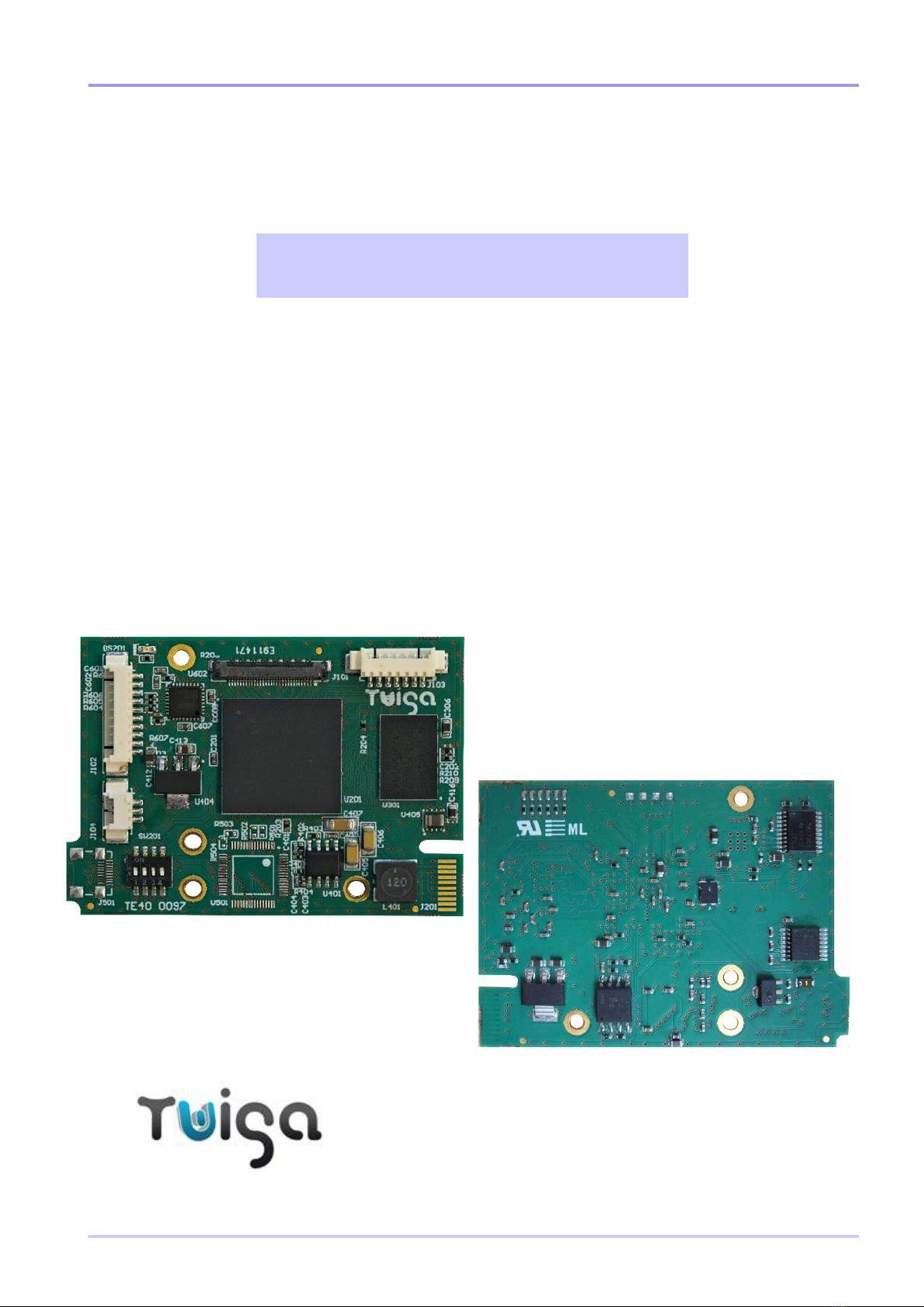
Technical manual – LVDS to YPbPr, CVBS converter board 3/9
Product overview
This board converts a LVDS HD video signal to component YPbPr or composite SD (PAL or NTSC).
Format supported are 720p and 1080p/i – up to 1080p25/30 for YPbPr.
The composite SD video corresponds to complete area of the HD 1080p25 or 1080p30 view with letter
box or cropped option to realize 16/9 to 4/3 adaptation.
Output mode is selected with micro switches.
The remote configuration of the camera with a serial communication - TTL or RS232 level - is in
accordance with VISCA protocol.
Synoptics
1. Main functions
•LVDS signal decoding (with FPGA)
•Memorization of the SD image to realize NTSC or PAL interlacing
•SD NTSC / PAL Signal scaling (FPGA)
•NTSC & PAL Coding (SD video encoder)
•YPbPr digital to analog conversion
•TTL/RS232 for remote control
•Power supply of the camera (8 to 12V), and of the board functions (1.2V, 1.8V and 3.3V)
Specifications
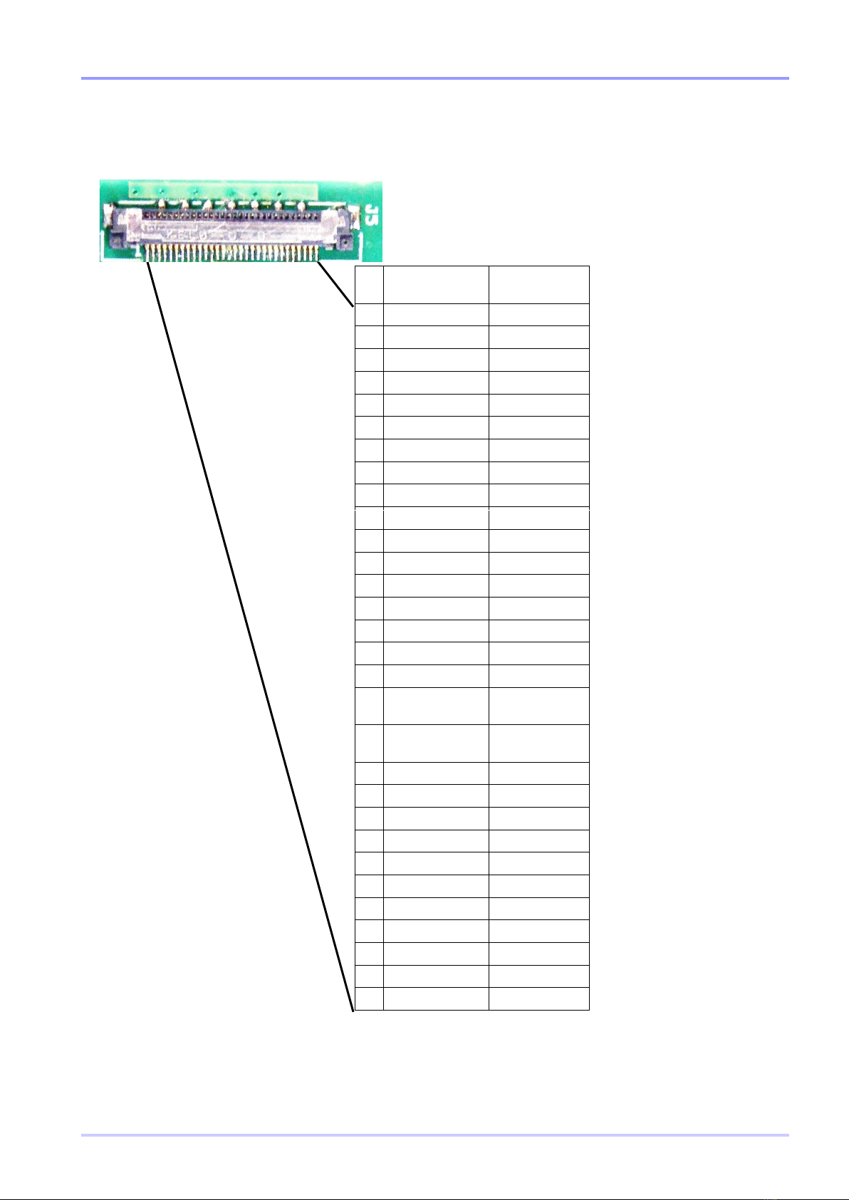
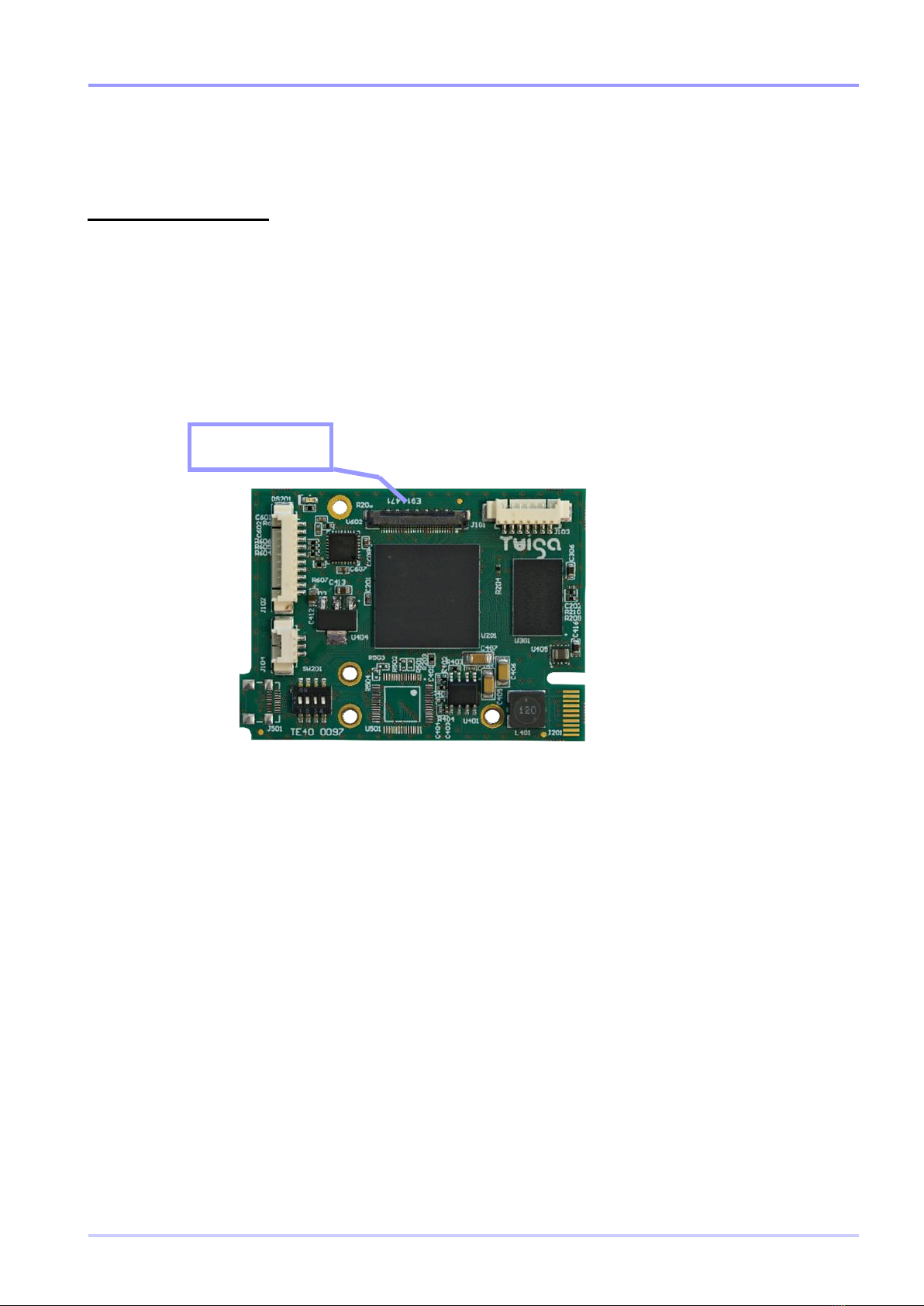
2. LVDS camera input
•LVDS (Y, Cb, Cr, Sync, Clk) 5 channels 8 bits (“Channel link format”)
•LVDS clock: 74,25MHz or 148,5MHz
•HD video formats: 720p50/60, 1080p25/30, 1080i50/60, 1080p50/60
•KEL 30 ways connector
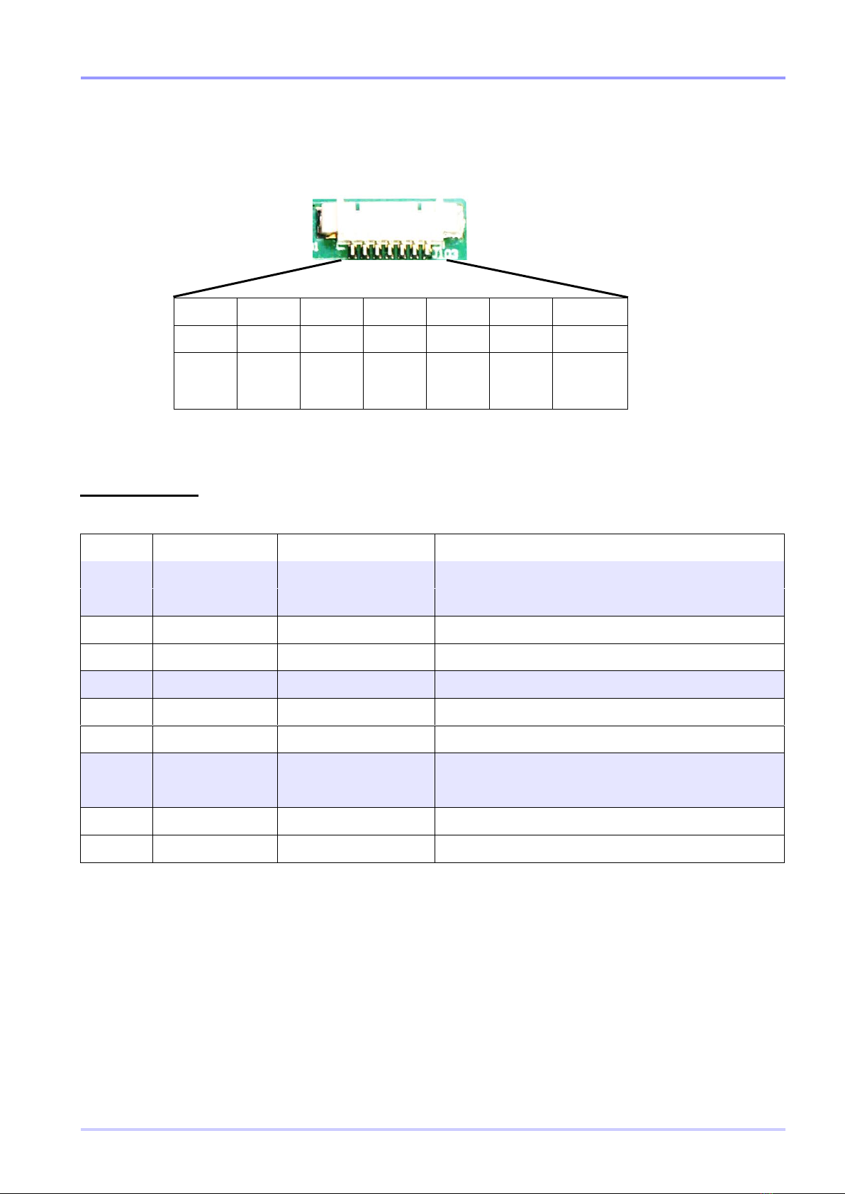
3. SD Analog Outputs
•VBS and YC :1V pp, 75ohm
•NTSC (with 1080p30/29,97 or 1080p60/59,94 configuration)
•PAL (with 1080p25 or 1080p50 configuration)
•“Letter box” or “crop” conversion from HD 16/9 to SD 4/3 aspect ratio
•Delay from LVDS inputs to analog outputs: about 40ms for PAL and moving from 33ms to
67ms for NTSC
•MOLEX 10 ways connector
4. HD Analog Outputs
•YPbPr :1V pp, 75ohm
•From 720p50 to 1080p30 video formats
•MOLEX 10 ways connector
5. Serial control
•VISCA (SONY) protocol
•Baud rate: 9600, 19200, 38400, 115200
•Logical level +3V3 on MOLEX 10 ways connector
•RS232 level on MOLEX 3 ways connector

Technical manual – LVDS to YPbPr, CVBS converter board 4/9
6. GPI control
•Zoom, focus and freeze controls
•Connection to ground to activate the control.
•Logical level +3V3
•MOLEX 7 ways connector
7. Power
•+8 to 12V voltage, about 5W consumption with camera
•MOLEX 10 ways connector
8. Mechanical
•Board dimensions: 55mm x 41,5mm
•Four 2,2mm diameter mounting holes

Technical manual – LVDS to YPbPr, CVBS converter board 5/9
Board connections
Connectors pinout
9. Analog video, RS, power (J102)
MOLEX 53261-1071 connector
1
Y / CVBS
2
0V-GND
3
TxD-TTL (board input)
4
RxD-TTL (board output)
5
0V-GND
6
+8 to 12V
7
0V-GND
8
Pr / S-video (C)
9
0V-GND
10
Pb / S-video (Y)
10. RS 232 (J104)
MOLEX 53261-0371 connector
1
0V-GND
2
RxD-232 (board output)
3
TxD-232 (board input)
LVDS source
GPI Controls
- VBS Output
- YC Output
- Serial link
- Power
RS232
DIP Switches

Technical manual – LVDS to YPbPr, CVBS converter board 6/9
11. LVDS camera (J101)
KEL USL00-30L Connector
LVDS 4
channels
LVDS 8
channels
30
NC
TX4-
29
NC
TX4+
28
NC
TX5-
27
NC
TX5+
26
Reset
Reset
25
NC
NC
24
NC
TX6-
23
NC
TX6+
22
NC
TX7-
21
NC
TX7+
20
0V-GND
0V-GND
19
0V-GND
0V-GND
18
+V
+V
17
+V
+V
16
+V
+V
15
+V
+V
14
+V
+V
13
RxD (TTL
camera input)
RxD (TTL
camera input)
12
TxD (TTL
camera output)
TxD ( TTL
camera output)
11
0V-GND
0V-GND
10
TX0-
TX0-
9
TX0+
TX0+
8
TX1-
TX1-
7
TX1+
TX1+
6
TX2-
TX2-
5
TX2+
TX2+
4
TXCLKOUT-
TXCLKOUT-
3
TXCLKOUT+
TXCLKOUT+
2
TX3-
TX3-
1
TX3+
TX3+

Technical manual – LVDS to YPbPr, CVBS converter board 7/9
12. GPI controls (J103)
MOLEX 53261-0771 Connector
7
6
5
4
3
2
1
Ctrl6
Ctrl5
Ctrl4
Ctrl3
Ctrl2
Ctrl1
0V-GND
Freeze
Focus far
Focus
near
Focus
Auto/
Manual
Zoom -
Zoom +
GPI controls
Pin
Action
Control
VISCA command (hexa)
Ctrl1
Press
Zoom +
81 01 04 07 23 FF
Release
Zoom stop
81 01 04 07 00 FF
Ctrl 2
Press
Zoom -
81 01 04 07 33 FF
Release
Zoom stop
81 01 04 07 00 FF
Ctrl 3
Press
Focus auto/manual
81 01 04 38 10 FF
Ctrl 4
Press
Focus near
81 01 04 08 30 FF
Release
Focus stop
81 01 04 08 00 FF
Ctrl 5
Press
Focus far
81 01 04 08 20 FF
Release
Focus stop
81 01 04 08 00 FF
Ctrl 6
Press
Image freeze
81 01 04 62 02 FF
Next press
End of freeze
81 01 04 62 03 FF
A control is activated (= Press) when the pin is grounded, it is deactivated (= Release) when the pin is
unconnected.

Technical manual – LVDS to YPbPr, CVBS converter board 8/9
Output modes selection
YPbPr output
when SW2 = OFF and SW1 = ON
SD output
when SW2 = ON and SW1 = OFF
SW3 selects 16/9 to 4/3 conversion:
➢«Letter box » aspect ratio
No part of HD view is cut, black horizontal bars are added on top and bottom of SD output
This mode is selected when SW4 switch is OFF
➢«Crop » aspect ratio
Left and right sides of HD view are cut, whole high is preserved on SD output.
This mode is selected when SW4 switch is ON
➢«Squeeze » aspect ratio
16/9 HD video content converted to 4/3 SD output resulting in vertical elongation,
This mode is selected when SW3 switch is ON
SD
720
576 – PAL
483 - NTSC
or

Technical manual – LVDS to YPbPr, CVBS converter board 9/9
LED signalization
During initialization phase, led blinking indicates the state of the board:
•1 flash every 2 seconds: waiting for RX pin ready
•2 flashes every 2 seconds: waiting for message reception (3s time out)
•3 flashes every 2 seconds: camera baud rate measurement
•4 flashes every 2 seconds: camera identification
•5 flashes every 2 seconds: initialization OK
LED indicator
Table of contents
Other Twiga Computer Hardware manuals
Popular Computer Hardware manuals by other brands

Mitsubishi Electric
Mitsubishi Electric 800 Series instruction manual

PINBALL TECHNOLOGY
PINBALL TECHNOLOGY NW7 user manual

KUULAIRE
KUULAIRE KA12 owner's manual

Pepperl+Fuchs
Pepperl+Fuchs HiSHPTB/32/TR-AI-01 Product installation manual

Excalibur
Excalibur DAS-429PCI/Mx user manual

Epson
Epson S1C88655 Technical manual