Carrier Board Design Guide for VIA QSM-8Q60
iv
Table of Contents
1. Introduction ...................................................................................................................................1
1.1. Document Overview.........................................................................................................................................1
1.2. Acronyms and Definitions ...............................................................................................................................2
1.3. Illustrations and Schematics............................................................................................................................3
2. General Carrier Board Recommendations ...............................................................................4
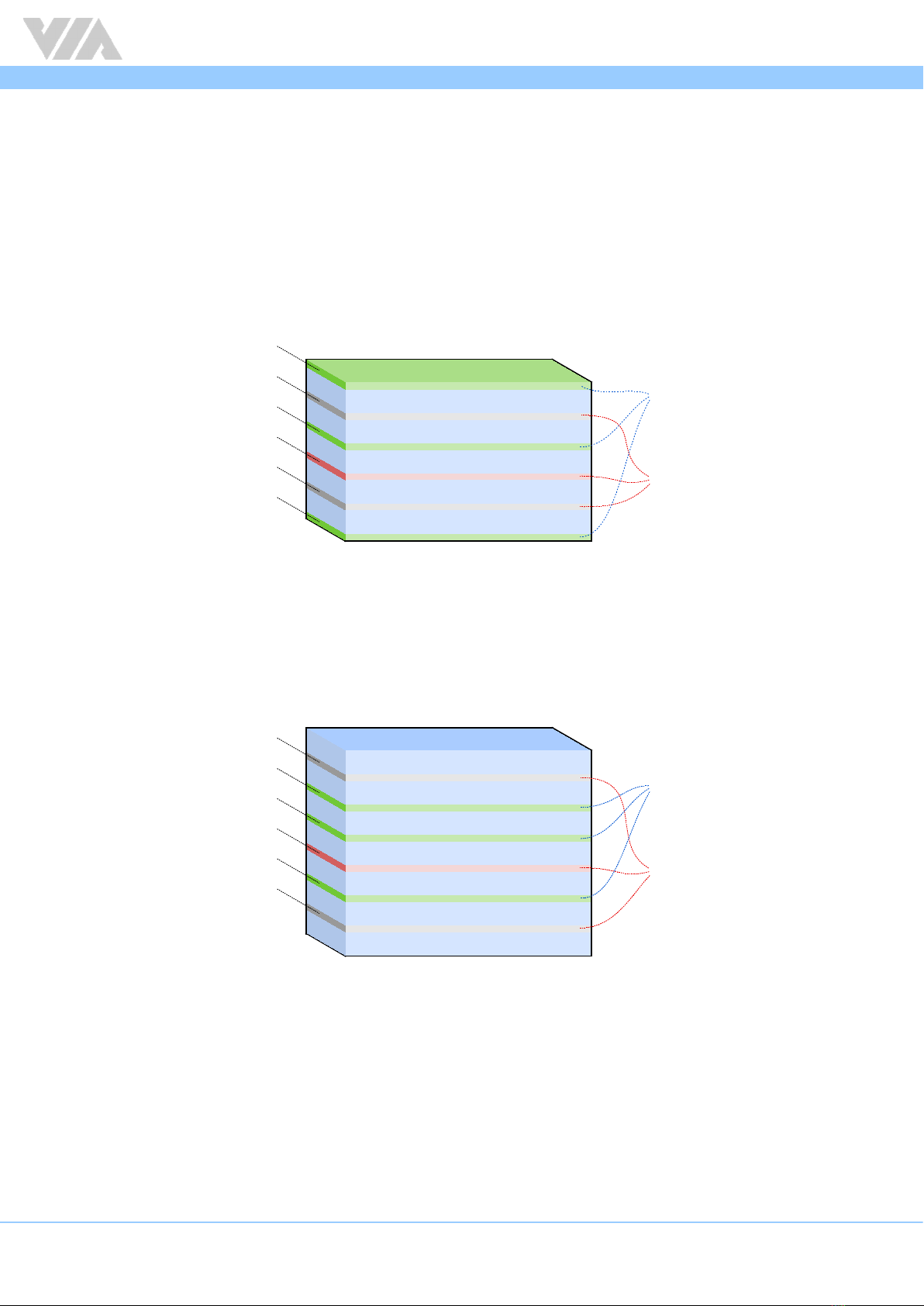
2.1. PCB Stackup Example.......................................................................................................................................4
2.1.1. Microstrip Versus Stripline Designs .......................................................................................................4
2.2. General Layout and Routing Guidelines ......................................................................................................6
2.2.1. Routing Styles and Topology ..................................................................................................................6
2.2.2. General Trace Attribute Recommendations ........................................................................................7
2.2.3. General Clock Routing Considerations .................................................................................................7
3. Qseven Specification Overview.................................................................................................9
3.1. Qseven Module Placement.............................................................................................................................9
3.2. Qseven Mechanical Characteristics...............................................................................................................9
3.3. VIA QSM-8Q60 Module and Carrier Board Dimensions........................................................................... 10
3.4.MXM Connector ............................................................................................................................................. 11
3.4.1. MXM Connector Dimensions................................................................................................................ 11
3.4.2. MXM Connector Footprint .................................................................................................................... 12
3.4.3. VIA QSM-8Q60 Module and MXM Connector Footprint ............................................................. 12
3.5. MXM Connector Pinouts............................................................................................................................... 13
4. Layout and Routing Recommendations ..................................................................................17
4.1. PCI Express Interface ..................................................................................................................................... 17
4.1.1. MiniPCIe Slot............................................................................................................................................ 17
4.1.2. PCI Express Layout and Routing Recommendations ....................................................................... 19
4.1.3. PCI Express Reference Schematics ...................................................................................................... 20
4.2. Ethernet Interface ........................................................................................................................................... 21
4.2.1. Ethernet Interface Topology................................................................................................................. 22
4.2.2. Gigabit Ethernet Layout and Routing Recommendations............................................................... 23
4.2.3. Gigabit Ethernet Reference Schematics ............................................................................................. 24
4.3. USB Interface ................................................................................................................................................... 25
4.3.1. USB Layout and Routing Recommendations ..................................................................................... 25
4.3.2. USB Reference Schematics.................................................................................................................... 28
4.4. LVDS Interface................................................................................................................................................. 29
4.4.1. LVDS Layout and Routing Recommendations................................................................................... 30
4.4.2. LVDS Reference Schematics ................................................................................................................. 32
4.5. HDMI Interface ................................................................................................................................................ 33
4.5.1. HDMI Layout and Routing Recommendations.................................................................................. 34
4.5.2. HDMI Reference Schematics................................................................................................................. 35
4.6. Audio Interface ............................................................................................................................................... 36
4.6.1. Audio Layout and Routing Recommendations ................................................................................. 36
4.6.2. Audio Reference Schematics ................................................................................................................ 37