2.4 VK16K33 SOP24 Pin Description
February 2020Rev. 1.26/27
www.szvinka.com
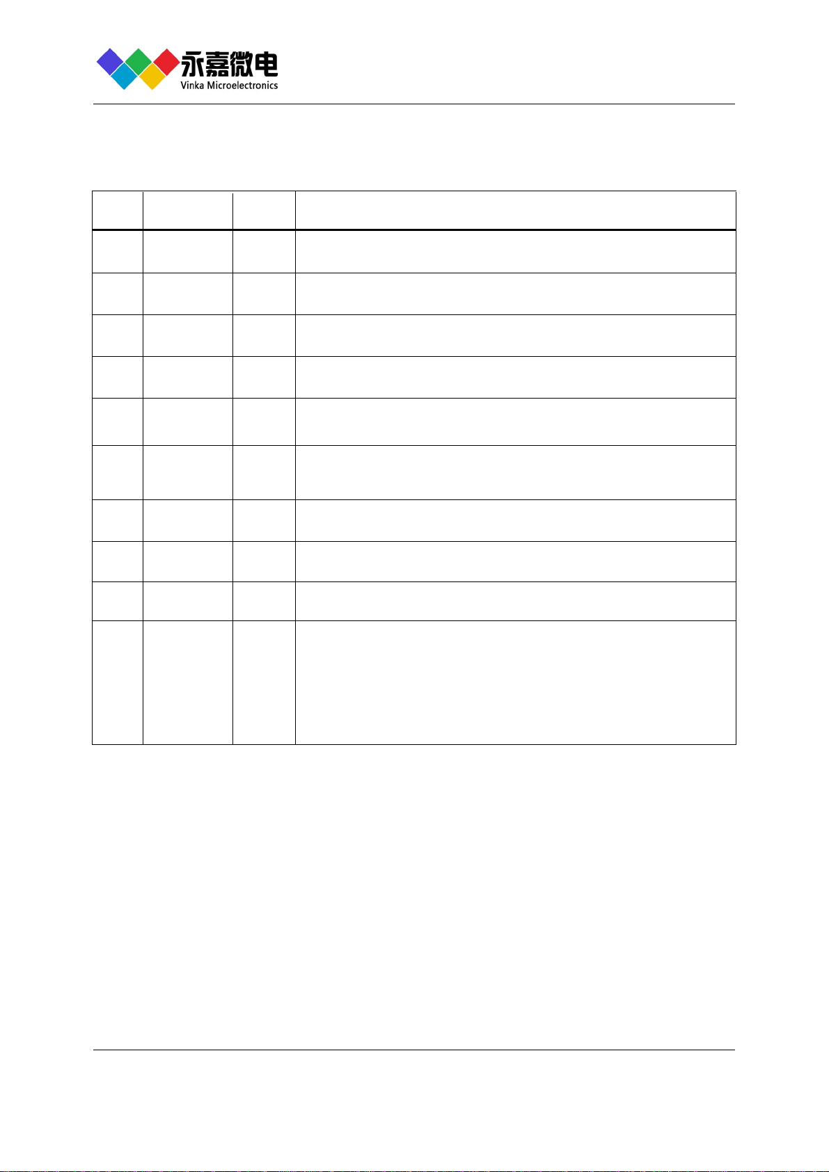
O
VSS
11-19 I/O
SEG10/K9-
SEG2/K1
22 O
SCL
GRID1/KS0-
GRID3/KS2
6~9 OLED GRID outputs(N-MOS open drain )
Serial Clock Input for I2C interface
2GRID0/AD
Negative power supply
3-5
1VSS
O
I/O
SDA
24 VDD
VDD
Serial Data Input/Output for I2C interface
Positive power supply
23
GRID4 ~GRID7
10 SEG11/K10
/INT I/O
20-21 SEG1/A0-
SEG0/A1 I/O LED SEG outputs(P-MOS open drain )
I2C slave address setting pin, 4 address 0xe0-0xe3 can be set,
and bit0 is the read / write bit. *1
LED GRID outputs(N-MOS open drain );
Key source output pin, active high during key scan operation
LED SEG outputs(P-MOS open drain );
Key data input pin, internal pull-low during key scan operation
LED GRID outputs(N-MOS open drain )
I2C slave address source output pin, active high during power on and key scan *1
*1 I2C slave address is selected through A2-A0 pins, and I2C slave address is updated during power on reset
or key scanning cycle
VK16K33
16×8 LED DRIVER
No. I/O
Name Function
I. when bit0 of SEG / INT register is set to“ 0”,this pin is LED SEG output(P-
MOS open drain )and Key data input during key scan operation.
II. when bit0 of SEG / INT register is set to“ 1”,this pin is Interrupt signal (INT)
output pin
bit1 of SEG/INT register is set to“ 0”,INT pin output active-low
bit1 of SEG/INT register is set to“ 1”,INT pin output active-high