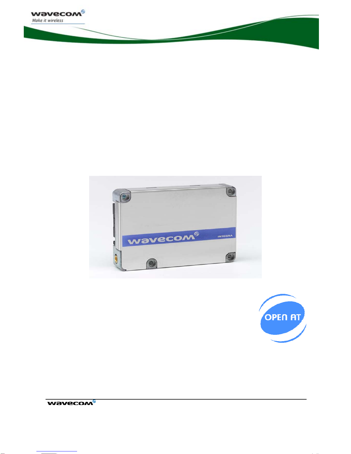
Wavecom Integra M2106+ Owner's manual

©Confidential Page: 1 / 77
This document is the sole and exclusive property of Wavecom. Not to be distributed or divulged without prior written
agreement.
WA_DEV_M2106+_PTS_003-001 April, 2007
Plug & Play Wireless CPU®
Integra M2106+
Product Specification
Reference: WA_DEV_M2106+_PTS_003
Revision: 001
Date: April, 2007
Supports Open AT®embedded ANSI C applications

Integra M2106+
©Confidential Page: 2 / 77
This document is the sole and exclusive property of Wavecom. Not to be distributed or divulged without prior written
agreement.
WA_DEV_M2106+_PTS_003-001 April, 2007
Document Information
Revision Date History of the evolution
001 April 2007 Creation

Integra M2106+
©Confidential Page: 3 / 77
This document is the sole and exclusive property of Wavecom. Not to be distributed or divulged without prior written
agreement.
WA_DEV_M2106+_PTS_003-001 April, 2007
Caution
Information furnished herein by Wavecom is accurate and reliable. However, no responsibility is assumed for
its use. Please read carefully the safety precautions for an application based on the Integra M2106+
Wireless CPU®.
Trademarks
WAVECOM®, Open AT®,Wireless CPU®are trademarks or registered trademarks of WAVECOM SA. All
other company and/or product names mentioned may be trademarks or registered trademarks of their
respective owners.
Copyright
This manual is copyrighted by WAVECOM with all rights reserved. No part of this manual may be
reproduced in any form without the prior written permission of WAVECOM. No patent liability is assumed
with respect to the use of the information contained herein.

Integra M2106+
©Confidential Page: 4 / 77
This document is the sole and exclusive property of Wavecom. Not to be distributed or divulged without prior written
agreement.
WA_DEV_M2106+_PTS_003-001 April, 2007
Web Site Support
General information about Wavecom and its range of
products:
www.wavecom.com
Carrier/Operator approvals: www.wavecom.com/approvals
Open AT®Introduction: www.wavecom.com/OpenAT
Developer support for software and hardware: www.wavecom.com/forum

Integra M2106+
©Confidential Page: 5 / 77
This document is the sole and exclusive property of Wavecom. Not to be distributed or divulged without prior written
agreement.
WA_DEV_M2106+_PTS_003-001 April, 2007
Overview
This document defines and specifies the Integra M2106+ Plug & Play Wireless CPU®. It also contains
guidelines for application design and recommendations to use the Integra development kit.
This Plug and Play Wireless CPU®is an E-GSM/GSM - GPRS Class 10 900/1800 product, based on the
Q24 Wireless CPU®which supports Open AT®by default.
Open AT®is the world’s most comprehensive cellular development environment, which allows embedded
standard ANSI C applications to be natively executed directly on the Wireless CPU®.
This Product Specification document covers the Wireless CPU®alone and does not include the
programmable capabilities provided via the use of Open AT®Software Suites.
For detailed software programming guides, refer to the documents shown in the “Reference Documents”
section.

Integra M2106+
©Confidential Page: 6 / 77
This document is the sole and exclusive property of Wavecom. Not to be distributed or divulged without prior written
agreement.
WA_DEV_M2106+_PTS_003-001 April, 2007
Contents
1References ........................................................................................................................................... 10
1.1 Reference Documents........................................................................................................................... 10
1.1.1 Open AT®Software Documentation............................................................................................ 10
1.1.2 AT Software Documentation ....................................................................................................... 10
1.1.3 Other Documents ........................................................................................................................ 10
2General Description ............................................................................................................................ 13
2.1 Presentation .......................................................................................................................................... 13
2.2 Key Features ......................................................................................................................................... 14
2.3 Difference between M2106B and M2106+ Wireless CPU®.................................................................. 14
2.4 GSM/GPRS Services ............................................................................................................................ 15
2.5 Functional Description........................................................................................................................... 16
2.5.1 Block Diagram............................................................................................................................. 16
2.5.2 RF Functionalities ....................................................................................................................... 17
2.5.3 Firmware ..................................................................................................................................... 17
2.6 CE Conformity ....................................................................................................................................... 17
2.7 RoHS Compliance................................................................................................................................. 17
3Interfaces.............................................................................................................................................. 18
3.1 General Purpose Connector.................................................................................................................. 18
3.1.1 Pin Allocation .............................................................................................................................. 19
3.1.2 Signal Description ....................................................................................................................... 20
3.2 Power Supply ........................................................................................................................................ 22
3.3 ON/~OFF Control .................................................................................................................................. 24
3.3.1 General Description .................................................................................................................... 24
3.3.2 Operating Sequences ................................................................................................................. 25
3.4 Alternative Download Control (BOOT pin) ............................................................................................ 28
3.5 Reset Signal (~RST) ............................................................................................................................. 29
3.5.1 General Presentation .................................................................................................................. 29
3.5.2 Reset Sequence.......................................................................................................................... 30
3.6 Serial Link.............................................................................................................................................. 31
3.6.1 Interface Description ................................................................................................................... 31
3.6.2 Application Note with Level Shifter .............................................................................................32
3.7 SPI Bus.................................................................................................................................................. 32
3.8 Keyboard Interface ................................................................................................................................ 33
3.9 Audio Interface ...................................................................................................................................... 34
3.9.1 Microphone Inputs....................................................................................................................... 34
3.9.2 Speaker Outputs ......................................................................................................................... 36
3.10 General Purpose Input/Output .............................................................................................................. 38
3.11 Analog to Digital Converter (ADC) ........................................................................................................ 39

Integra M2106+
©Confidential Page: 7 / 77
This document is the sole and exclusive property of Wavecom. Not to be distributed or divulged without prior written
agreement.
WA_DEV_M2106+_PTS_003-001 April, 2007
3.12 Activity Status Indication (Flashing LED) .............................................................................................. 39
3.13 RF Interface........................................................................................................................................... 41
3.13.1 RF Interface Characteristics........................................................................................................ 41
3.13.2 RF Performance.......................................................................................................................... 41
3.13.3 Antenna Specifications................................................................................................................ 42
3.14 SIM Card Interface ................................................................................................................................ 43
3.14.1 Internal SIM Card Interface......................................................................................................... 44
3.14.2 External SIM Card Interface........................................................................................................ 45
4Technical Specifications..................................................................................................................... 47
4.1 Environmental Constraints .................................................................................................................... 47
4.2 Mechanical Specifications ..................................................................................................................... 47
4.2.1 Mechanical Overview .................................................................................................................. 47
4.2.2 Mechanical Characteristics ......................................................................................................... 48
4.2.3 Mechanical Drawings .................................................................................................................. 48
4.3 Electrical Specifications......................................................................................................................... 50
4.3.1 Power Mode ................................................................................................................................ 50
4.3.2 Power Consumption without Open AT®Processing ................................................................... 51
4.3.3 Power Consumption with Open AT®Processing ........................................................................ 52
4.3.4 Current Consumption Waveform ................................................................................................ 53
5Applicable Normative Documents..................................................................................................... 54
5.1 Normative Specifications....................................................................................................................... 54
5.2 Environmental Specifications ................................................................................................................ 55
6Using the Integra Wireless CPU®....................................................................................................... 58
6.1 Firmware Upgrade................................................................................................................................. 58
6.1.1 Nominal Upgrade Procedure.......................................................................................................58
6.1.2 Alternative Procedure.................................................................................................................. 58
6.2 Guidelines for Application Design ......................................................................................................... 58
6.2.1 Hardware Recommendations...................................................................................................... 58
6.2.2 Antenna....................................................................................................................................... 59
6.2.3 Minimum Hardware Interface to Get Started .............................................................................. 59
6.3 3 V/5 V SIM Management ..................................................................................................................... 60
6.4 Installation of the Integra M2106+ Wireless CPU® on an Application Board ........................................ 61
6.5 Integra Development Kit Board Presentation........................................................................................ 63
6.5.1 Getting Started ............................................................................................................................ 64
6.5.2 Setting up Terminal Emulator...................................................................................................... 64
6.5.3 Example of AT Commands ......................................................................................................... 65
7Troubleshooting.................................................................................................................................. 68
7.1 Not Connecting Through the Serial Link ............................................................................................... 68
7.2 Receiving 'no carrier' Messages .......................................................................................................... 69
7.3 Receiving error Messages..................................................................................................................... 71

Integra M2106+
©Confidential Page: 8 / 77
This document is the sole and exclusive property of Wavecom. Not to be distributed or divulged without prior written
agreement.
WA_DEV_M2106+_PTS_003-001 April, 2007
8Annexes................................................................................................................................................ 73
8.1 Supplier Information .............................................................................................................................. 73
8.1.1 General Purpose Connector .......................................................................................................73
8.1.2 Antenna connector ...................................................................................................................... 74
8.1.3 SIM Card Holder ......................................................................................................................... 74
8.2 Safety Recommendations (for information only) ...................................................................................75
8.2.1 RF Safety .................................................................................................................................... 75
8.2.2 General safety............................................................................................................................. 76
8.2.3 Safety Standards......................................................................................................................... 77

Integra M2106+
©Confidential Page: 9 / 77
This document is the sole and exclusive property of Wavecom. Not to be distributed or divulged without prior written
agreement.
WA_DEV_M2106+_PTS_003-001 April, 2007
List of Figures
Figure 1: M2106+ view .................................................................................................................................... 13
Figure 2: Integra M2106+ Wireless CPU®connectors .................................................................................... 13
Figure 3: Functional architecture ..................................................................................................................... 16
Figure 4: 50-pin connector............................................................................................................................... 18
Figure 5: Pin allocation .................................................................................................................................... 19
Figure 6: Power-ON sequence diagram (no PIN code activated) ................................................................... 25
Figure 7: Power-OFF sequence diagram ........................................................................................................ 27
Figure 8: BOOT application schematic............................................................................................................ 28
Figure 9: Reset application schematic............................................................................................................. 29
Figure 10: Reset sequence diagram ............................................................................................................... 30
Figure 11: Level shifter application diagram for serial link* ............................................................................. 32
Figure 12: MIC2 input connection.................................................................................................................... 35
Figure 13: MIC1 differential connection........................................................................................................... 36
Figure 14: Speaker differential connection ...................................................................................................... 37
Figure 15: Speaker single-ended connection.................................................................................................. 37
Figure 16: SIM card holder extraction ............................................................................................................. 44
Figure 17: Schematic for external SIM card holder ......................................................................................... 46
Figure 18: Mechanical overview 1/3 ................................................................................................................ 47
Figure 19: Mechanical overview 2/3 ................................................................................................................ 47
Figure 20: Mechanical overview 3/3 ................................................................................................................ 48
Figure 21: Schematic for a SIM level shifter to manage 5 V SIM cards.......................................................... 60
Figure 22: Recommended footprint ................................................................................................................. 62
Figure 23: Integra development kit board description ..................................................................................... 63
Figure 24: High and low profile CLP connectors ............................................................................................. 73
Figure 25: Flexible flat cable (Part number: FFSD-20-S-10-01-N).................................................................. 73
Figure 26: Flex cable connector (Part number: FLE 125 01LDVA)................................................................. 73
Figure 27: MMCX connector example (right angle)......................................................................................... 74

Integra M2106+
Erreur ! Style non défini.
©Confidential Page: 10 / 77
This document is the sole and exclusive property of Wavecom. Not to be distributed or divulged without prior written
agreement.
WA_DEV_M2106+_PTS_003-001 April, 2007
1References
1.1 Reference Documents
Note: All below documents are related to V3.12 Open AT®Software and 6.57a Open AT®Firmware.
Wavecom recommends that the developer should check the web site for the latest documentation
1.1.1 Open AT®Software Documentation
[1] Getting started with Open AT®(Ref. WM_ASW_OAT_CTI_00001)
[2] Open AT®Tutorial (Ref. WM_ASW_OAT_UGD_00001)
[3] Tools Manual (Ref. WM_ASW_OAT_UGD_00003)
[4] Open AT®Basic Development Guide (Ref. WM_ASW_OAT_UGD_00002)
[5] Open AT®ADL guide (Ref. WM_ASW_OAT_UGD_00006)
[6] Open AT®V3.12 Customer Release Note (Ref. WM_DEV_OAT_DVD_165)
1.1.2 AT Software Documentation
[7] AT commands Interface Guide for X57 Release
(Ref. WM_ASW_OAT_UGD_00044)
[8] Open AT®6.57a FW Release Note (Ref. WM_DEV_OAT_DVD_237)
1.1.3 Other Documents
[9] Environmental conditions and environmental tests for telecommunication equipment - ETS 300 019
[10] Wavecom Acceptance and Verification Plan (Ref. WAVE Plan, Release 1.4)
[11] Power Consumption Modes Application note (Ref. WM_ASW_OAT_APN_012)
.

Integra M2106+
Erreur ! Style non défini.
©Confidential Page: 11 / 77
This document is the sole and exclusive property of Wavecom. Not to be distributed or divulged without prior written
agreement.
WA_DEV_M2106+_PTS_003-001 April, 2007
1.2 List of Abbreviations
Abbreviation Description
AC Alternating Current
ADC Analog to Digital Converter
A/D Analog to Digital conversion
AT ATtention (prefix for modem commands)
AUX AUXiliary
CBS Cell Broadcast Service
CLK CLocK
CMOS Complementary Metal Oxide Semiconductor
CTS Clear To Send
dB Decibel
DC Direct Current
DCD Data Carrier Detect
DCS Digital Cellular System
DSR Data Set Ready
DTR Data Terminal Ready
E-GSM Extended GSM
EN ENable
ESD ElectroStatic Discharges
ETSI European Telecommunications Standards Institute
GND GrouND
GPIO General Purpose Input Output
GPO General Purpose Output
GPRS General Packet Radio Service
GSM Global System for Mobile communications
Hi Z High impedance (Z)
I/O Input / Output
KSPS Kilo Samples Per Second
LED Light Emitting Diode
LSB Less Significant Bit
MAX MAXimum
MIC MICrophone
MIN MINimum
MO Mobile Originated
MS Mobile Station

Integra M2106+
Erreur ! Style non défini.
©Confidential Page: 12 / 77
This document is the sole and exclusive property of Wavecom. Not to be distributed or divulged without prior written
agreement.
WA_DEV_M2106+_PTS_003-001 April, 2007
MT Mobile Terminated
PC Personal Computer
PCB Printed Circuit Board
PCS Personal Communications Service
RAM Random Access Memory
RF Radio Frequency
RI Ring Indicator
RST ReSeT
RTS Request To Send
RX Receive
SAR Specific Absorption Rate
SIM Subscriber Identification Module
SMS Short Message Service
SPI Serial Peripheral Interface
SPK SPeaKer
SRAM Static RAM
TAC Type Approval Code
TDMA Time Division Multiple Access
TU Typical Urban fading profile
TUHigh Typical Urban, High speed fading profile
TVS Transient Voltage Suppressor
TX Transmit
TYP TYPical
UART Universal Asynchronous Receiver-Transmitter
USSD Unstructured Supplementary Service Data
VSWR Voltage Stationary Wave Ratio
WAP Wireless Application Protocol

Integra M2106+
Erreur ! Style non défini.
©Confidential Page: 13 / 77
This document is the sole and exclusive property of Wavecom. Not to be distributed or divulged without prior written
agreement.
WA_DEV_M2106+_PTS_003-001 April, 2007
2General Description
2.1 Presentation
The Integra M2106+ Wireless CPU®is a self-contained E-GSM/GSM-GPRS 900/1800 dual-band Wireless
CPU®and is GPRS class 10 capable.
Figure 1: M2106+ view
It includes a Quik Q24 Wireless CPU®and its interfaces are available through:
•A 50-pin connector for Baseband analog and digital interfaces (General Purpose Connector)
•A RF connector, MMCX type
•A SIM card holder
RF
connector
SIM card
holder
50-pin
connector
Figure 2: Integra M2106+ Wireless CPU®connectors
The mating connectors for the General Purpose connector and RF connector are standard and easy-to-find.

Integra M2106+
Erreur ! Style non défini.
©Confidential Page: 14 / 77
This document is the sole and exclusive property of Wavecom. Not to be distributed or divulged without prior written
agreement.
WA_DEV_M2106+_PTS_003-001 April, 2007
2.2 Key Features
Integra M2106+ Wireless CPU®features:
•Open AT®programmable:
o Native execution of embedded standard ANSI C applications,
o Custom AT command creation,
o Custom application library creation,
o Standalone operation.
•Overall dimensions: 46 x 64 x 12 mm,
•Complete shielding,
•2-Watt E-GSM 900 radio section,
•1-Watt GSM1800 radio section,
•Full GSM or GSM / GPRS software stack,
•GPRS class 10,
•32 Mbits of Flash memory and 16 Mbits of SRAM,
•Internal 3V/1.8V SIM interface,
•Real Time Clock (RTC) with calendar,
•Echo cancellation + noise reduction,
•Complete interfacing through a 50-pin General Purpose Connector:
o Power supply,
o Serial link,
o Audio interface,
o SIM card interface,
o Keyboard interface,
o GPIO.
2.3 Difference between M2106B and M2106+ Wireless CPU®
The Integra M2106+ Wireless CPU®is designed for replacing Integra M2106B Wireless CPU®. There are
some feature differences between these two.
M2106B Wireless CPU®M2106+ Wireless CPU®
SIM Interface 3V only 3V / 1V8
SRAM size 4 Mbits 16 Mbits
RF functionalities Dual band capability
(E-GSM900 / 1800)
Quad band capability*
(GSM850/ E-GSM900 / DCS1800 /
PCS1900)
Signal description -- I/O type and Reset state
See section 3.1.2 details
(*) See section 2.5.2 for further details

Integra M2106+
Erreur ! Style non défini.
©Confidential Page: 15 / 77
This document is the sole and exclusive property of Wavecom. Not to be distributed or divulged without prior written
agreement.
WA_DEV_M2106+_PTS_003-001 April, 2007
2.4 GSM/GPRS Services
The basic services provided by the Integra M2106+ Wireless CPU®are listed in the table below:
Standard •900 MHz, E-GSM compliant; Class 4 (2 W).
•1800 MHz ; Class 1 (1 W)
•GSM phase 2
•GPRS Class 10
Interface •Serial interface V.24/CMOS
•AT command set based on V.25ter and GSM 07.05 & 07.07.
•Auto-bauding function between 2400 bits/s and 19200 bits/s
•No auto-framing available
Audio •Half rate / Full rate / Enhanced Full rate operation
•Accessories (options): Handset, Car Kit
SMS •Mobile Originated (MO) and Mobile Terminated (MT)
•Mode Text & PDU point to point
•Cell broad cast
•In accordance with GSM 07.05
Data •Asynchronous 2400, 4800, 9600, 14400 bits/s
•Transparent and Non Transparent mode
•In Non Transparent Mode: 300, 1200, 1200/75 bauds
•Mode 3.1 kHz (PSTN) and V110 (ISDN)
Fax •2400/4800/7200/9600 bits/s, GSM teleservice 62 in Transparent Mode
•Class 1 & Class 2
•Group 3 compatible
GPRS
•Class 10
•Coding schemes: CS1 to CS4
•Compliant with SMG31bis
SIM •Plug-In SIM 3V/1.8V
•Full compatible with GSM 11.11
•SIM Toolkit Release 97

Integra M2106+
Erreur ! Style non défini.
©Confidential Page: 16 / 77
This document is the sole and exclusive property of Wavecom. Not to be distributed or divulged without prior written
agreement.
WA_DEV_M2106+_PTS_003-001 April, 2007
2.5 Functional Description
2.5.1 Block Diagram
Q24 W ireless
CPU®
Antenna
connector
Audio
Interface
Pow er
Supply
BOOT
RESET
50-pin
connector
SIM VCC
Microphone Microphone
Speaker Speaker
SIM card
Socket SIM card
Holder
Integra M2106+ Wireless CPU
®
Serial Interface
GPIO & ADC
SPI In terface
Ke
yp
ad Interface
O
p
eratin
g
Status Indication
VBat
Figure 3: Functional architecture

Integra M2106+
Erreur ! Style non défini.
©Confidential Page: 17 / 77
This document is the sole and exclusive property of Wavecom. Not to be distributed or divulged without prior written
agreement.
WA_DEV_M2106+_PTS_003-001 April, 2007
2.5.2 RF Functionalities
The Radio Frequency (RF) functionalities comply with the Phase II E-GSM 900 / DCS 1800
recommendations.
The frequencies are:
Transmit band (TX) Receive band (RX)
EGSM 900 880 to 915 MHz 925 to 960 MHz
DCS 1800 1710 to 1785 MHz 1805 to 915 MHz
The Integra M2106+ Wireless CPU®also gives a quad band capability (GSM850, EGSM900, DCS 1800 and
PCS 1900) and it is qualified by Wavecom.
Warning:
The Integra M2106+ Wireless CPU®is not certified for American market for operation band of
GSM850 and PCS1900. Customers wishing to sell the Integra M2106+ Wireless CPU®in American
region shall be wholly responsible for any certifications and carrier approval required.
2.5.3 Firmware
The Integra M2106+ Wireless CPU®is designed to integrate into various types of applications. For
applications using an external processor to control the Wireless CPU®, the firmware offers a software
interface based on AT commands.
A development kit for the Integra M2106+ Wireless CPU®is also available to test customer software
applications.
2.6 CE Conformity
The Integra M2106+ Wireless CPU®bears the CE marking. This symbol guarantees the compliance of the
design and implementation of the Integra M2106+ Wireless CPU®with the R&TTE directive.
2.7 RoHS Compliance
The Integra M2106+ Wireless CPU®is now compliant with RoHS (Restriction of Hazardous Substances in
Electrical and Electronic Equipment) Directive 2002/95/EC which sets limits for the use of certain restricted
hazardous substances. This directive states that “from 1st July 2006, new electrical and electronic equipment
put on the market does not contain lead, mercury, cadmium, hexavalent chromium, polybrominated
biphenyls (PBB), and polybrominated diphenyl ethers (PBDE)”.

Integra M2106+
Erreur ! Style non défini.
©Confidential Page: 18 / 77
This document is the sole and exclusive property of Wavecom. Not to be distributed or divulged without prior written
agreement.
WA_DEV_M2106+_PTS_003-001 April, 2007
3Interfaces
This chapter describes the hardware interfaces of the Integra M2106+ Wireless CPU®.
3.1 General Purpose Connector
A 50-pin standard connector provides the baseband analog and digital interfaces.
49
50
12
Figure 4: 50-pin connector

Integra M2106+
Erreur ! Style non défini.
©Confidential Page: 19 / 77
This document is the sole and exclusive property of Wavecom. Not to be distributed or divulged without prior written
agreement.
WA_DEV_M2106+_PTS_003-001 April, 2007
3.1.1 Pin Allocation
1
3
5
7
9
11
13
15
17
19
21
23
25
27
29
31
33
35
37
39
41
43
45
47
49
2
4
6
8
10
12
14
16
18
20
22
24
26
28
30
32
34
36
38
40
42
44
46
48
50
GND
+5V
GND
SPK2N
MIC2P
GND
GPIO0
CT104/RX
CT105/RTS
COL4
ROW 3
SPI EN
,
GPO3
SIM RST
SIM PRES1
GPO0
SPK2P
SPK1P
SPK1N
MIC2N
MIC1P
MIC1N
COL2
COL0
ROW 1
SPI CLK
GND
+ 5 V
CT109/DCD
GPIO4
ON/~ OFF
BOOT
CT103/TX
CT107/DSR
CT108-2/DTR
COL3
ROW 2
NC
SIM CLK
SIM VCC
SIM DATA
CT125/RI
FLASHING LED
CT106/CTS
AUXV0
~RST
GND
COL1
ROW 4
ROW 0
SPI IO
Figure 5: Pin allocation

Integra M2106+
Erreur ! Style non défini.
©Confidential Page: 20 / 77
This document is the sole and exclusive property of Wavecom. Not to be distributed or divulged without prior written
agreement.
WA_DEV_M2106+_PTS_003-001 April, 2007
3.1.2 Signal Description
The following table presents the main characteristics of the 50-pin connector.
Pin
# Name I/O Reset
State I/O type Description Comment
1 GND -- Ground High current
2 GND -- Ground High current
3 + 5 V I -- Supply High current
4 + 5 V I -- Supply High current
5 CT109/DCD O High Z 2X Serial Link
Data Carrier Detect
6 GND -- Ground High current
7 GPIO4 I/O High Z CMOS/2X General Purpose I/O
8 SPK2N O High Z Analog
Speaker2 negative
output
9 CT125/RI O High Z 2X Serial Link
Ring Indicator
10 SPK2P O High Z Analog Speaker 2
positive output
11 Flashing LED I/O High Z CMOS/2X Operating mode
indication LED
Driven by Wireless
CPU®
12 SPK1P O High Z Analog Speaker 1
positive output
13 CT106/CTS O High Z 1X Serial Link
Clear To Send
14 SPK1N O High Z Analog Speaker 1
negative output
15 ON/~OFF I Pull down -- Power control signal ON = VCC
16 MIC2P I High Z Analog Microphone 2
positive input
17 AUXV0 I HZ Analog Auxiliary ADC input Can be tied to GND if
not used
18 MIC2N I High Z Analog Microphone 2
negative input
19 ~RST I/O -- SCHMITT Reset active low
To be driven by an
Open Collector.
Internal pull-up
4.7 kΩ.
20 MIC1P I High Z Analog Microphone 1
positive input
21 GND -- Ground High Current
22 MIC1N I High Z Analog Microphone 1
negative input
Table of contents
Other Wavecom Computer Hardware manuals
Popular Computer Hardware manuals by other brands

National Semiconductor
National Semiconductor Data Capture Board CLC-CAPT-PCASM user guide

Renesas
Renesas SIMPLE DEMO quick start guide

NZXT
NZXT H7 ELITE manual

WIN Enterprises
WIN Enterprises PL-01030 user manual

ATI Technologies
ATI Technologies ATP8500.1 Owner's manual addendum

Roland
Roland World SR-JV80-05 owner's manual