WIN Enterprises MB-73240 User manual

User’s Manual
WIN Enterprises, Inc. All rights reserved. Mar. 2012
1
MB-73240
Embedded Board
PC/104+ module with Intel ® Atom™ 1.8GHz D525, LVDS, 2 LAN, SATA, CFast
User’s Manual
Version 1.0

User’s Manual
WIN Enterprises, Inc. All rights reserved. Mar. 2012
2
© Copyright 2012. All Rights Reserved
Manual Edition 1.0, March, 2012
This document contains proprietary information protected by copyright. All
rights are reserved; no part of this manual may be reproduced, copied,
translated or transmitted in any form or by any means without prior written
permission of the manufacturer.
The content of this document is intended to be accurate and reliable; the
original manufacturer assumes no responsibility for any inaccuracies that may
be contained in this manual. The original manufacturer reserves the right to
make improvements to the products described in this manual at any time
without prior notice.
Trademarks
IBM, EGA, VGA, XT/AT, OS/2 and PS/2 are registered trademarks of
International business Machine Corporation
Award is a trademark of Award Software International, Inc
Intel is a trademark of Intel
RTL is a trademark of Realtek
VIA is a trademark of VIA Technologies, Inc
Microsoft, Windows, Windows NT and MS-DOS are either trademarks or
registered trademarks of Microsoft Corporation
All other product names mentioned herein are used for identification purpose
only and may be trademarks and/or registered trademarks of their respective
companies
Limitation of Liability
While reasonable efforts have been made to ensure the accuracy of this
document, the manufacturer and distributor assume no liability resulting from
errors or omissions in this document, or from the use of the information
contained herein.
For more information on MB-73240 or other WIN Enterprises products, please
visit our website http://www.win-ent.com.

User’s Manual
WIN Enterprises, Inc. All rights reserved. Mar. 2012
3
Table of Contents
Safety information............................................................................................. 5
Electrical safety................................................................................................. 5
Operation safety................................................................................................ 5
Statement.......................................................................................................... 6
Packing list........................................................................................................ 6
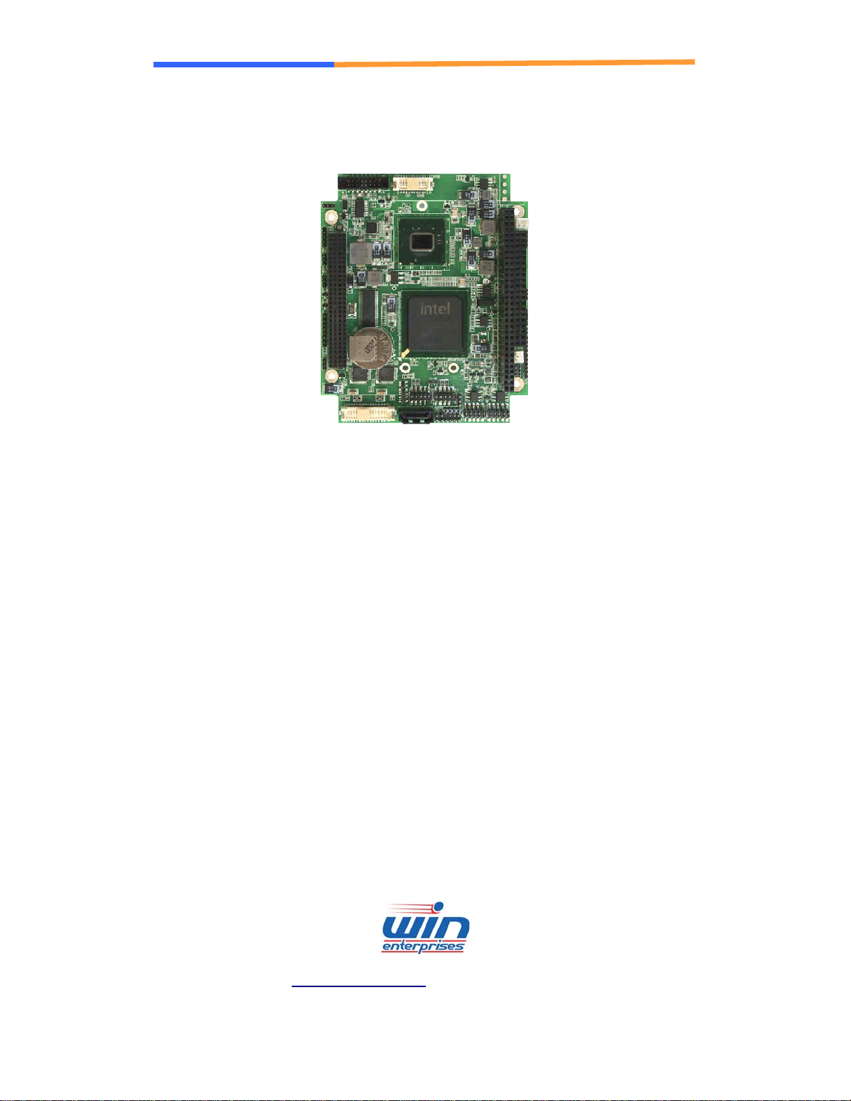
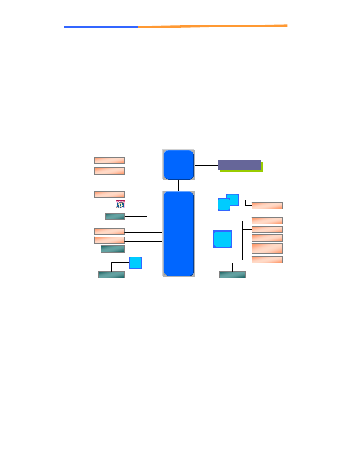
Chapter 1 Product Information.......................................................................... 7
1.1 Block Diagram............................................................................................. 7
1.2 Key Features............................................................................................... 8
1.3 Board Placement ...................................................................................... 10
Chapter 2 Jumpers and Connectors............................................................... 12
2.1 Connector ................................................................................................. 12
CN1: VGA Connector (Pin Header)................................................................ 12
CN2: LVDS CONNECTOR ............................................................................. 13
CN3: AT POWER CONNECTOR.................................................................... 13
CN4: AUX POWER CONNECOTR ................................................................ 13
CN5: Flat Panel Inverter Connector ............................................................... 13
CN6: ATX POWER CONNECOTR................................................................. 13
CN7: PC/104 Plus Connector......................................................................... 14
CN8: Auxiliary Power Connector.................................................................... 14
CN9: Power LED /HDD LED/Reset/Speak Out Connector............................ 15
CN10: ATX Power Control Connector ............................................................ 15
CN12: FAN Connector.................................................................................... 15
CN13 GPIO Connector................................................................................... 15
CN14, CN15: USB1/2, USB3/4 Connector (Pin Header)............................... 16
CN16: COM2 –RS422/RS485 Connector (Pin Header)................................. 16
CN18: CN17: COM1, COM2 RS-232 Pin-Header.......................................... 16
CN19: LAN1, LAN2 Interface.......................................................................... 16
CN20: SATAconnector................................................................................... 17
CN21: Audio Interface..................................................................................... 17
CN22: CFAST................................................................................................. 17
CN23: PC/104 Connector............................................................................... 18
2.2 Jumper setting………………………………………………………………….19
Chapter 3 BIOS Setup.................................................................................... 20
3.1 Entering the CMOS Setup Program......................................................... 20
3.2 Menu Options............................................................................................ 22
3.3 Advanced Menu........................................................................................ 23

User’s Manual
WIN Enterprises, Inc. All rights reserved. Mar. 2012
4
3.3.1 CPU Configuration................................................................................. 24
3.3.2 IDE Configuration .................................................................................. 25
3.3.3 Super IO Configuration.......................................................................... 26
3.3.4 Hardware Health Configuration............................................................. 27
3.3.5 ACPI Configuration ................................................................................ 28
3.3.6 AHCI Configuration................................................................................ 32
3.3.7 ISA Configuration................................................................................... 34
3.3.8 USB Configuration................................................................................. 36
3.4 PCIPnP Menu ........................................................................................... 37
3.5 Boot Menu................................................................................................. 39
3.5.1 Boot Settings Configuration................................................................... 40
3.6 Security Menu........................................................................................... 41
3.7 Chipset Menu............................................................................................ 43
3.7.1 North Bridge Configuration.................................................................... 44
3.7.2 South Bridge Configuration ................................................................... 46
3.8 Exit............................................................................................................ 47

User’s Manual
WIN Enterprises, Inc. All rights reserved. Mar. 2012
5
Safety information
Electrical safety
yTo prevent electrical shock hazard disconnect the power cable from the
electrical outlet before relocating the system.
yWhen adding or removing devices to or from the system ensure that the
power cables for the devices are unplugged before the signal cables are
connected. If possible, disconnect all power cables from the existing system
before you add a device.
yBefore connecting or removing signal cables from the motherboard make
sure that all the power cables are unplugged.
ySeek professional assistance before using an adapter or extension cord.
These devices could interfere with the grounding circuit.
yMake sure that your power supply is set to the correct voltage in your area.
yIf you are not sure about the voltage of the electrical outlet you are using
contact your local power company.
yIf the power supply is broken do not try to fix it by yourself. Contact a qualified
service technician or your retailer.
Operational safety
yBefore installing the motherboard and adding devices carefully read all the
manuals that came with the package.
yBefore using the product make sure all cables are correctly connected and
the power cables are not damaged. If you detect any damage contact your
dealer immediately.
yTo avoid short circuits keep paper clips, screws, and staples away from
connectors, slots, sockets and circuitry.
yAvoid dust, humidity, and temperature extremes. Do not place the product in
an area where it may become wet.
yDeploy the product on a stable surface.
yIf you encounter technical problems with the product contact a qualified
service technician or your retailer.

User’s Manual
WIN Enterprises, Inc. All rights reserved. Mar. 2012
6
Statement
yAll rights reserved. No part of this publication may be reproduced in any form
or by any means, without prior written permission from the publisher.
yAll trademarks are the properties of the respective owners.
yAll product specifications are subject to change without prior notice
Packing list
□ 1 x MB-73240
□ 1 x CD (Driver & User’s Manual)
□ 1 x Dual RJ-45 connector adaptor card (optional)
□ 1 x Cable Kit (optional)
y1 x ATX power cable
y1 x RS-232 cable
y1 x VGA cable
y1 x USB cable

User’s Manual
WIN Enterprises, Inc. All rights reserved. Mar. 2012
7
Chapter 1. Product Information
1.1 Block Diagram
Support processor list:
Intel D525 1.8GHz/2C4T/1M/13W
Intel D425 1.8GHz/1C2T/512K/10W
Intel N455 1.6GHz/1C2T/512K/6.5W
DMI
SATA to IDE
2 PCI-e x1
CFast
VGA (pin header)
SATA
USB 2.0
LVDS 18bits
DDR3-800/667MHz
SO-DIMM x1
Intel
Pine view
Rea l
t
R212A Dual RJ45
LVDS (pin header)
VGA
SATA
SPI BIOS SPI
4x USB (pin header)
HDA
Audio (HDA header)
PCI/104
Mini PC
I
-e
LPC
PCI-e x1 & USB
PC/104
Rea l
t
ISA Bus
SATA
PCI Bus
PCI to ISA
ITE 8
8
Watch Dog Timer
H/W Monitor
COM1(RS232)
COM2
(RS232/422/48
GPIO x8
PCI Bus
Intel
ICH8-M
SMSC
SCH31
12
S

User’s Manual
WIN Enterprises, Inc. All rights reserved. Mar. 2012
8
1.2 Key Features
■
■
Features:
zSupports powerful dual-core Intel®Atom™ D525 processors
zDual 10/100/1000Mbps ethernet
zSupports One cFast, Two serial ports and four USB 2.0 ports
zOne DDR3 SO-DIMM socket supports up to 2GB memory
zSupports SM bus w/ Alert
■
■System
CPU Intel® Atom D525, D425
BIOS AMI® SPI BIOS
System Chipset Intel® ICH8M
System Memory 1 x DDR3 SO-DIMM socket supports 667/800MHz memory max. up
to 2GB w/o ECC registered
SSD 1 x CFast
Watchdog Timer 255 levels timer interval, (1sec. to 255min.), setup by software.
Expansion Interface 1 x PCI104, 1 x PC104
Battery Lithium 3V/220mAH
■
■I/O
I/O Interface 1 x SATA, 1 x RS-232, 1 x RS-232/422/485
USB 4 x USB 2.0
Audio High definition audio interface
GPIO Onboard programmable 8-bit Digital I/Os
■
■Ethernet
Speed 10/100/1000Mbps
Interface 2 x RJ-45
Ethernet Interface IEEE 802.3 10/100/1000 Mbps compliant physical layer
■
■
Display
Chipset Intel® Pineview-D processor Integrated
Memory Size TBD
Resolution VGA: 2048 x 1536
LCD/LVDS Interface LVDS: 1366 x 768 18-bit LVDS
Dual Simultaneous
Displays VGA+ LVDS
■
■Mechanical and Environment
Dimension ( L x W ) 96mm (L) x 116mm (W)
(3.8” L x 4.6” W)
PC/104+ Form Factor
Operating Temperature 0°C ~ 60°C ( 32°F ~ 140°F )
Operating Humidity 10% ~ 85% relative humidity, non-condensing
Storage Temperature -20°C ~ 85°C ( -4°F ~ 185°F )
Storage Humidity 10% ~ 85% relative humidity, non-condensing

User’s Manual
WIN Enterprises, Inc. All rights reserved. Mar. 2012
9
■
■Power
Power Supply Voltage +5V DC in
Power Consumption TBD
■
■Packing List
z1 x MB-73240 SBC
z1 x CD (Manual, Quick installation guide, Utility driver)
■
■Ordering Information
Standard
MB‐7324A PC/104+modulewithIntelAtom1.8GHzD525,LVDS,2LAN,
SATA,CFast
MB‐7324B PC/104+modulewithIntelAtom1.8GHzD425,LVDS,2LAN,
SATA,CFast
MB‐7324C PC/104+modulewithIntelAtom1.8GHzD525,LVDS,2LAN,
SATA,CFast(pindown)
MB‐7324D PC/104+modulewithIntelAtom1.8GHzD425,LVDS,2LAN,
SATA,CFast(pindown)
All specifications and photos are subject to change without notice*

User’s Manual
WIN Enterprises, Inc. All rights reserved. Mar. 2012
10
1.3 Board Placement

User’s Manual
WIN Enterprises, Inc. All rights reserved. Mar. 2012
11

User’s Manual
WIN Enterprises, Inc. All rights reserved. Mar. 2012
12
Chapter 2. Jumpers and Connectors
2.1 Connector
CN1: VGA Connector (Pin Header)
Pin Signal Pin Signal
1 RED 2 GREEN
3 BLUE 4 +5V
5 GND 6 GND
7 GND 8 GND
9 +5V 10 GND
11 +5V 12 DDC Data
13 H-SYNC 14 V-SYNC
15 DDC Clock 16 NC

User’s Manual
WIN Enterprises, Inc. All rights reserved. Mar. 2012
13
CN2: LVDS CONNECTOR
Pin Define Pin Define
1 LVDS_D0+ 2 LVDS_D0-
3 GND 4 GND
5 LVDS_D1+ 6 LVDS_D1-
7 GND 8 PANEL POWER
9 LVDS_D2+ 10 LVDS_D2-
11 LVDS_CLK+ 12 LVDS_CLK-
13 GND 14 GND
15 NC 16 NC
17 LVDS_BKTEN 18 PANEL POWER
19 LVDS_SDA 20 LVDS_SCL
CN3: AT POWER CONNECTOR
Pin Define Pin Define
1 +5V 2 +5V
3 GND 4 GND
CN4: AUX POWER CONNECOTR
Pin Define Pin Define
1 GND 2 +12V
CN5: Flat Panel Inverter Connector
Pin Assignment
1 +12V
2 GND
3 FPBKLEN
4 VR
5 +5V
CN6: ATX POWER CONNECOTR
Pin Define Pin Define
1 +5Vstby 2 +5Vstby
3 GND PSON#

User’s Manual
WIN Enterprises, Inc. All rights reserved. Mar. 2012
14
CN7: PC/104 Plus Connector
Signal Pin Signal Pin Signal Pin Signal Pin
GND A1 NC B1 +5V C1 AD00 D1
VIO A2 AD02 B2 AD01 C2 +5V D2
AD05 A3 GND B3 AD04 C3 AD03 D3
C/BE0# A4 AD07 B4 GND C4 AD06 D4
GND A5 AD09 B5 AD08 C5 GND D5
AD11 A6 VIO B6 AD10 C6 M66EN D6
AD14 A7 AD13 B7 GND C7 AD12 D7
+3.3V A8 C/BE1# B8 AD15 C8 +3.3V D8
SERR# A9 GND B9 SBO# C9 PAR D9
GND A10 PERR# B10 +3.3V C10 SDONE D10
STOP# A11 +3.3V B11 LOCK# C11 GND D11
+3.3V A12 TRDY# B12 GND C12 DEVSEL# D12
FRAME# A13 GND B13 IRDY# C13 +3.3V D13
GND A14 AD16 B14 +3.3V C14 C/BE2# D14
AD18 A15 +3.3V B15 AD17 C15 GND D15
AD21 A16 AD20 B16 GND C16 AD19 D16
+3.3V A17 AD23 B17 AD22 C17 +3.3V D17
IDSEL0 A18 GND B18 IDSEL1 C18 IDSEL2 D18
AD24 A19 C/BE3# B19 VIO C19 IDSEL3 D19
GND A20 AD26 B20 AD25 C20 GND D20
AD29 A21 +5V B21 AD28 C21 AD27 D21
+5V A22 AD30 B22 GND C22 AD31 D22
REQ0# A23 GND B23 REQ1# C23 VIO D23
GND A24 REQ2# B24 +5V C24 GNT0# D24
GNT1# A25 VIO B25 GNT2# C25 GND D25
+5V A26 CLK0 B26 GND C26 CLK1 D26
CLK2 A27 +5V B27 CLK3 C27 GND D27
Ground A28 INTD# B28 +5V C28 RST# D28
+12V A29 INTA# B29 INTB# C29 INTC# D29
-12V A30 REQ3# B30 GNT3# C30 GND D30
CN8: Auxiliary Power Connector
Pin Assignment
1 -5V
2 GND
3 Key pin
4 -12V

User’s Manual
WIN Enterprises, Inc. All rights reserved. Mar. 2012
15
CN9: Power LED /HDD LED/Reset/Speak Out Connector
Pin Assignment
1 Power LED+
2 Power LED-
3 HDD LED+
4 HDD LED-
5 Reset +
6 Reset -
7 Speak Out+
8 Speak Out-
CN10: ATX Power Control Connector
Pin Assignment
1 PANSW-
2 PANSW+
CN12: FAN Connector
CN13 GPIO Connector
Pin Assignment
1 +3.3V
2 GPIO0
3 GPIO1
4 GPIO2
5 GPIO3
6 GPIO4
7 GPIO5
8 GPIO6
9 GPIO7
10 GND
Pin Define Pin Define
1 +5V 2 GND

User’s Manual
WIN Enterprises, Inc. All rights reserved. Mar. 2012
16
CN14, CN15: USB1/2, USB3/4 Connector (Pin Header)
Pin Assignment Pin Assignment
1 +5V 2 +5V
3 Data0- 4 Data1-
5 Data0+ 6 Data1+
7 GND 8 GND
9 Key Pin 10 GND
CN16: COM2 –RS422/RS485 Connector (Pin Header)
Pin Assignment
1 485RXD-
2 485RXD+
3 485TXD+
4 485TXD-
CN18: CN17: COM1, COM2 RS-232 Pin-Header
Pin Assignment Pin Assignment
1 DCD 2 DSR
2 RXD 4 RTS
3 TXD 6 CTS
4 DTR 8 RI
5 GND 10 NC
CN19: LAN1, LAN2 Interface
Pin Signal Pin Signal
1 LAN1-D2+ 2 LAN1-D0+
3 LAN1-D2- 4 LAN1-D0-
5 LAN1-D3+ 6 LAN1-D1+
7 LAN1-D3- 8 LAN1-D1-
9 +3.3V 10 GND
11 LAN1-ACT 12 LAN1-LINK
13 LAN1_LINK100 14 LAN1-LINK1000
15 GND 16 GND
17 LAN2-D0+ 18 LAN2-D2+
19 LAN2-D0- 20 LAN2-D2-
21 LAN2-D1+ 22 LAN2-D3+
23 LAN2-D1- 24 LAN2-D3-
25 LAN2-ACT 26 LAN2-LINK
27 LAN2_LINK100 28 LAN2-LINK1000
29 GND 30 GND

User’s Manual
WIN Enterprises, Inc. All rights reserved. Mar. 2012
17
CN20: SATA connector
Pin Signal Name
1 GND
2 TX+
3 TX-
4 GND
5 RX-
6 RX+
7 GND
CN21: Audio Interface
Pin Assignment Pin Assignment
1 +5V 2 GND
3 GND 4 CLKBIT
5 +3.3V 6 Key Pin
7 SDTAIN 8 SYNC
9 GND 10 PRST#
11 SDATAOUT 12 NC
CN22: CFAST
Signal segment Power segment
Pin Name Pin Name
S1 GND PC1 CDI
S2 A+ PC2 GND
S3 A- PC3 TBD
S4 GND PC4 TBD
S5 B- PC5 TBD
S6 B+ PC6 TBD
S7 GND PC7 GND
PC8* LED1
PC9* LED2
PC10 IO1
PC11 IO2
PC12 IO3
PC13 PWR
PC14 PWR
PC15 PGND
PC16 PGND
PC17 CDO
*Refer above for LED output design guide

User’s Manual
WIN Enterprises, Inc. All rights reserved. Mar. 2012
18
CN23: PC/104 Connector
Signal Pin Signal Pin Signal Pin Signal Pin
GND C0 GND D0 IOCHCHK A1 GND B1
SBHE* C1 MEMCS16* D1 SD7 A2 RESET B2
LA23 C2 IOSC16* D2 SD6 A3 +5V B3
LA22 C3 IRQ10 D3 SD5 A4 IRQ9 B4
LA21 C4 IRQ11 D4 SD4 A5 -5V B5
LA20 C5 IRQ12 D5 SD3 A6 NC B6
LA19 C6 IRQ15 D6 SD2 A7 -12V B7
LA18 C7 IRQ14 D7 SD1 A8 0 wait state B8
LA17 C8 NC D8 SD0 A9 +12V B9
MEMR* C9 NC D9 IOCHRDY A10 NC B10
MEMW* C10 NC D10 AEN A11 SMEMW# B11
SD8 C11 NC D11 SA19 A12 SMEMR* B12
SD9 C12 NC D12 SA18 A13 IOW* B13
SD10 C13 NC D13 SA17 A14 IOR* B14
SD11 C14 NC D14 SA16 A15 NC B15
SD12 C15 NC D15 SA15 A16 NC B16
SD13 C16 +5V D16 SA14 A17 NC B17
SD14 C17 MASTER* D17 SA13 A18 NC B18
SD15 C18 GND D18 SA12 A19 REFRESH* B19
NC C19 GND D19 SA11 A20 SYSCLK B20
SA10 A21 IRQ7 B21
SA9 A22 IRQ6 B22
SA8 A23 IRQ5 B23
SA7 A24 IRQ4 B24
SA6 A25 IRQ3 B25
SA5 A26 NC B26
SA4 A27 TC B27
SA3 A28 BALE B28
SA2 A29 +5V B29
SA1 A30 OSC B30
SA0 A31 GND B31
GND A32 GND B32

User’s Manual
WIN Enterprises, Inc. All rights reserved. Mar. 2012
19
2.2 Jump setting
JP1 LCD Power Select. (1-2: +3.3V ; 2-3: +5V)
JP2 PCI VIO Voltage Select
(1-2: +5V ; 2-3: +3.3V)
JP3 WDT Function Select.
(1-2: IRQ11 ; 2-3: Reset)
JP4 Clear CMOS
(1-2: Hold CMOS; 2-3: Clear CMOS)
JP5 AT & ATX MODE SELECT
(1-2:AT MODE ; 2-3: ATX MODE)
JP6 COM2 MODE SELECT
(1-2: RS232 ; 3-4: RS485 4-Wire ; 5-6: RS485 2-Wire)
JP7 PSON# Signal Souce Select.
(1-2: ICH8M ; 2-3: SIO)

User’s Manual
WIN Enterprises, Inc. All rights reserved. Mar. 2012
20
Chapter 3. BIOS Setup
3.1 Entering the CMOS Setup Program
Use the CMOS Setup program to modify the system parameters to reflect the
options installed in your system and to customize your system. For
example, you should run the Setup program after you:
1.Received an error code at startup
2.Install another disk drive
3.Use your system after not having used it for a long time
4.Find the original setup missing
5.Replace the battery
6.Change to a different type of CPU
7.Run the Flash program to update the system BIOS
Run the CMOS Setup program after you turn on the system. On-screen
instructions explain how to use the program.
Enter the CMOS Setup program’s main menu as follows:
1. Turn on or reboot the system. After the BIOS performs a series of
diagnostic checks, the following message appears:
“Press DEL to enter SETUP”
2. Press the <DEL> key to enter CMOS Setup program. The main menu
appears:
3. Choose a setup option with the arrow keys and press <Enter>. See the
following sections for a brief description of each setup option.
Table of contents
Other WIN Enterprises Control Unit manuals
Popular Control Unit manuals by other brands

Kessel
Kessel Staufix Series Installation and operating instructions

Karel
Karel DSS10-28 Technical reference and user's guide

A.R.I.
A.R.I. D-025 Installation operation & maintenance

HOT Display Technology
HOT Display Technology HTM160160E user manual

Delabie
Delabie 510140 quick start guide

GOK
GOK Caramatic ProTwo Assembly and operating manual