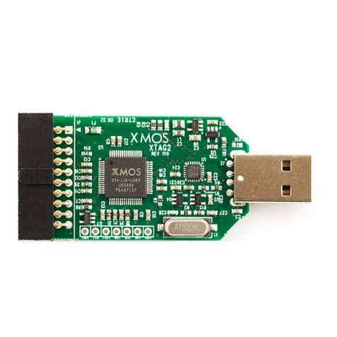
XMOS xTAG v3.0 User manual

Chipsmall Limited consists of a professional team with an average of over 10 year of expertise in the distribution
of electronic components. Based in Hongkong, we have already established firm and mutual-benefit business
relationships with customers from,Europe,America and south Asia,supplying obsolete and hard-to-find components
to meet their specific needs.
With the principle of “Quality Parts,Customers Priority,Honest Operation,and Considerate Service”,our business
mainly focus on the distribution of electronic components. Line cards we deal with include
Microchip,ALPS,ROHM,Xilinx,Pulse,ON,Everlight and Freescale. Main products comprise
IC,Modules,Potentiometer,IC Socket,Relay,Connector.Our parts cover such applications as commercial,industrial,
and automotives areas.
We are looking forward to setting up business relationship with you and hope to provide you with the best service
and solution. Let us make a better world for our industry!
Contact us
Tel: +86-755-8981 8866 Fax: +86-755-8427 6832
Email & Skype: [email protected]om Web: www.chipsmall.com
Address: A1208, Overseas Decoration Building, #122 Zhenhua RD., Futian, Shenzhen, China

xTAG v3.0 Hardware Manual
IN THIS DOCUMENT
·Introduction
·XS1-U8 device
·xSYS Connector (J2)
·J3 and J4 connectors
·24MHz Crystal Oscillator
·I/O Port-to-Pin Mapping
·xTAG v3.0 Schematic
1 Introduction
The xTAG v3.0 debug adapter converts between an XMOS XSYS connector and USB
2.0, providing pins for JTAG control, system reset, processor debug, one duplex
UART link and one duplex serial XMOS Link. The xTAG v3.0 debug adapter can
be used to connect XMOS development kits to most PCs, and provide a 5V power
supply from a USB 2.0 port.
The diagram below shows the layout of the components on the card.
20-way
IDC xSYS
connector
Standard
USB-B
connector
LEDs
J1
J3 J4
J2
Figure 1:
xTAG v3.0
features
To debug a board with the xTAG v3.0 you must use xTIMEcomposer 13.1 or later,
available from the XMOS web site: http://xmos.com/downloads.
The board requires an XMOS xSYS connector.
Publication Date: 2015/6/1 Document Number: XM006125A
XMOS © 2015, All Rights Reserved

xTAG v3.0 Hardware Manual 2/8
2 XS1-U8 device
The xTAG v3.0 is based on a single XS1-U8 device in a BGA package. The XS1-U8
consists of a single xCORE, which comprises a multicore microcontroller with
tightly integrated general purpose I/O pins and 64 KBytes of on-chip RAM. The
pins are brought out of the package and connected to the card’s components as
follows:
·
USB Connector (J1) The xTAG v3.0 uses a Standard B-type micro USB connector
to link to a PC. The USB connector is connected to the XS1-U8 device.
·xSYS 20-way IDC header
The processor has ports that are directly connected to the I/O pins. Six LEDs are
driven by the debugger, their function (clockwise, starting from the power button
on the bottom right):
Power Green The xTAG is powered on
Run Green Target is running
Red Target is in debug mode and stopped
Status Green Target stop reason is expected e.g. breakpoint,
print message
Red Target stop reason is unexpected e.g. exception
Target Green
Target device is detected after a Run Configuration
or Debug Configuration is used (xrun or xgdb
command)
Red Target device is not detected after a Run
Configuration or Debug Configuration is used
(xrun or xgdb command)
xSCOPE Green Flashing xSCOPE is enabled
Off No xSCOPE
JTAG Green There is JTAG activity with the target happening
Off No JTAG
3 xSYS Connector (J2)
The xTAG v3.0 includes an xSYS 20-way IDC header, which can be used to connect
it to an XMOS development board for debugging programs on the hardware.
The xSYS connector provides pins for JTAG control, system reset, processor debug,
a duplex UART link and a 2-bit serial xCONNECT Link.
XM006125A
xTAG v3.0 Hardware Manual 3/8
Pin Signal Direction Description
1 5V Target to Host Power
2 NC N/A No connection
3 MSEL Host to Target Select boot from JTAG - Active Low
4 GND N/A Ground
5 TDSRC Host to Target JTAG Test Data
6 XL1_UP1 Target to Host xCONNECT Link
7 TMS Host to Target JTAG Test Mode Select
8 GND N/A Ground
9 TCK Host to Target JTAG Test Clock
10 XL1_UP0 Target to Host xCONNECT Link
11 DEBUG Bidirectional Debug
12 GND N/A Ground
13 TDSNK Target to Host JTAG Test Data
14 XL1_DN0 Host to Target xCONNECT Link
15 RST_N Host to Target System Reset - Active Low
16 GND N/A Ground
17 UART_RX Host to Target Serial Port
18 XL1_DN1 Host to Target xCONNECT Link
19 UART_TX Target to Host Serial Port
20 GND N/A Ground
The routing of these I/O pins along with the power pins is shown below.
3.1 xCONNECT Link configuration
Some of the I/O pins on the processor are configured as a duplex 2-bit serial
xCONNECT Link. The mapping of xCONNECT Link to the pins is shown in the table
below:
XM006125A

xTAG v3.0 Hardware Manual 4/8
5V
MSEL
TDSCR
TMS
TCK
DEBUG
TDSNK
RST_N
UART_RX
UART_TX
1 2
19 20
NC
GND
XL1_UP1
GND
XL1-_UP0
GND
XL1-DN0
GND
XL1-DN1
GND
Figure 2:
xTAG v3.0
xSYS pinout
Pin xCONNECT Link
X0D52 XL1_UP1
X0D53 XL1_UP0
X0D54 XL1_DN0
X0D55 XL1_DN1
3.2 JTAG Configuration
Some of the I/O pins on the microcontroller are driven by the JTAG signals. The
mapping of the signals to the pins is shown in the table below:
Pin Port Processor
X0D11 P1D0 TDSRC
X0D13 P1F0 TDSNK
X0D22 P1G0 TMS
X0D10 P1C0 TCK
X0D70 P32A19 MSEL
XM006125A

xTAG v3.0 Hardware Manual 5/8
3.3 System Reset
The system reset signal is mapped to a 1-bit port on the processor as described
below. It is used as an output to reset the target processor from the debugger
Pin Port Processor
X0D50 P32A1 RST_N
4 J3 and J4 connectors
The xTAG v3.0 has two additional connectors. These are reserved for future use.
5 24MHz Crystal Oscillator
The XS1-U8 is clocked at 24MHz by a crystal oscillator on the card. The processor
is clocked at 500MHz and the I/O ports at 100MHz, by an on-chip phase locked
loop (PLL).
XM006125A

xTAG v3.0 Hardware Manual 6/8
6 I/O Port-to-Pin Mapping
The table below provides a full description of the port-to-pin mappings described
throughout this document.
Pin Port Processor
1b 8b 32b
X0D0 P1A0 UART_UP
X0D10 P1C0 TCK
X0D11 P1D0 TDSRC
X0D12 P1E0
X0D13 P1F0 TDSNK
X0D14 P8B0 LED
X0D15 P8B1 LED
X0D16 P8B2 LED
X0D17 P8B3 LED
X0D18 P8B4 LED
X0D19 P8B5 LED
X0D20 P8B6 LED
X0D21 P8B7 LED
X0D22 P1G0 TMS
X0D50 P32A1 RST_N
X0D51 P32A2 DBG
X0D52 P32A3 XL1_UP1
X0D53 P32A4 XL1_UP0
X0D54 P32A5 XL1_DN0
X0D55 P32A6 XL1_DN1
X0D69 P32A19 UART_DN
X0D70 P32A20 MSEL
XM006125A

xTAG v3.0 Hardware Manual 7/8
7 xTAG v3.0 Schematic
Copyright © XMOS Ltd 2012
Project Name
Size Sheet Name Rev
Sheet ofDate 25/02/2014
1V2B
1 1
xTAG3
XTAG3.PrjPCB
A3
XS1_U8A_FB96
VDDIO M6
VDDIO M7
VDDIO L6
VSS
E5
VSS
E6
VSS
E7
VSS
E8
VSS
F5
VSS
F6
VSS
F7
VSS
F8
VSS
G5
VSS
G6
VSS
G7
VSS
G8
VSS
H5
VSS
H6
VSS
H7
VSS
H8
SW1 J1
VSUP
M1
VDDCORE K1
PGND L1
SW2 M5
VDD1V8 M4
PGND M3
SW1 J2
VSUP
M2
VDDCORE K2
PGND L2
VSUP
H1
U1A
XS1_U8A_FB96
XI/CLK
E1
DEBUG_N
E2
MODE0
L5
MODE1
L4
MODE2
B5
MODE3
B6
RST_N
C2
TCK
C1
TDI
D2 TDO
B1
TMS
D1
X0D0 A9
X0D10 A10
X0D11 B10
X0D12 A11
X0D13 M12
X0D14 L11
X0D15 M11
X0D16 L10
X0D17 M10
X0D18 L9
X0D1 B9
X0D19 M9
X0D20 L8
X0D21 M8
X0D35 A8
X0D49 A12
X0D50 B11
X0D51 B12
X0D52 C11
X0D53 C12
X0D54 D11
X0D55 D12
X0D56 E11
X0D57 E12
X0D58 F11
X0D61 F12
X0D62 G11
X0D63 G12
X0D64 H11
X0D65 H12
X0D66 J11
X0D67 J12
X0D68 K11
X0D69 K12
X0D70 L12
XO
F1
USB_DP
A5
USB_DN
A6
USB_VBUS
A7
USB_ID
B7
ADC_IN0
A2
ADC_IN1
B2
ADC_IN2
A3
ADC_IN3
B3
AVDD
A1
X0D24 B8
NC
L3
NC
A4
X0D43/WAKE G1
OSC_EXT_N
F2
NC
H2
NC
G2
NC
B4
X0D22 L7
U1B
GND GND
100N
C3
100N
C2
4U7
C1
5V
GND GND GND
3V3
4U7
L1
4U7
L2
22U
C4
22U
C5
GND GND
RST_N_LOC
TCK_LOC
TMS_LOC
TDI_LOC
TDO_LOC
GND
3V3A
USB_DP
USB_DN
TCK
100N
C9
100N
C10
GND
1N
C13
100N
C11
100N
C12
330R
XXA
FB1
GND GND
5V
GND
GND
USB_DN
USB_DP
TMS
TDSNK
DIG_IN0
LED0
LED1
LED2
LED3
DIG_IN1
SRST_N
DBG
XL_DN1
XL_DN0
MSEL
ADC_IN0
ADC_IN1
ADC_IN2
ADC_IN3
5V
GND GND
3V3
1V8
GND
1V0
UGND
FEM_HEADER_RA
10
8
6
4
2
9
7
5
3
15
13
11 12
14
16
1
17
19
18
20
J2
0.35A
F1
5V
GND
MSEL
TDSRC
TMS
TCK
DBG
TDSNK
SRST_N
UART_DN
UART_UP
XL_UP1
XL_UP0
XL_DN0
XL_DN1
NA
3
2
1
4
6
5
7
J4
GND
TDO_LOC
TDI_LOC
RST_N_LOC
UART_DN
3V3
LED0
LED1
LED2
LED3
33R
R4
33R
R3
33R
R2
GND GND
1U
C8
1U
C15
1U
C14
10N
C16
GND
3V3A
GND GND
INA214
GND
2
IN_N
5OUT 6
IN_P
4
REF 1
VP 3
U2
XT3 DNF
GND
3V3A
GND
ADC_IN0
ADC_IN0_P
ADC_IN0_N 100N
C17
XT3 DNF
GND
3V3A
INA214
GND
2
IN_N
5OUT 6
IN_P
4
REF 1
VP 3
U4
XT3 DNF
GND
3V3A
GND
ADC_IN1
ADC_IN1_P
ADC_IN1_N 100N
C18
XT3 DNF
GND
3V3A
10K
8 1
R6A XT3 DNF 10K
72
R6B XT3 DNF
10K
6 3
R6C
XT3 DNF 10K
54
R6D XT3 DNF
GND
SMBJ5.0A
D5
XT3 DNF
SMBJ5.0A
D6
XT3 DNF
GND GND
ADC_IN2
ADC_IN3
ADC_IN0_P
ADC_IN0_N
ADC_IN1_P
ADC_IN1_N
ADC_IN2
ADC_IN3
DIG_IN0
DIG_IN1
GND
24M
XRCGB
X1
2P
C6
2P
C7
MSEL_LOC
MSEL_LOC
KSC421J
1A 2A
2B1B
SW1
XT3 DNF
GND
BUT
10K
R7
XT3 DNF
3V3
VIN
3
EN
6
BYP
1GND 2
VOUT2 5
VOUT1 4
U3
MIC5321
IDC_HEADER_MAL
10
8
6
4
2
9
7
5
3
15
13
11 12
14
16
1
J3
XT3 DNF
TDSRC
TMS_LOC
TCK_LOC
7 2
470R R1B
8 1
470R R1A
5 4
470R R1D
6 3
470R R1C
1 3
2 4
D2
1 3
2 4
D3
XL_UP1
XL_UP0
VBUS 1
D- 2
D+ 3
ID 4
GND 5
SH
6
SH
7
SH
8
SH
9
SH
10
SH
11
J1
USB_MICROB
UART_UP
PTH_M3
MTH1
3V3
LED4
LED5
LED6
LED7
1 3
2 4
D1
GREEN
D4
GREEN
D8
GREEND7
470R
R5
3V3
GND
BUT
LED4
LED5
LED6
LED7
5 4
470R R8D
6 3
470R R8C
7 2
470R R8B
8 1
470R R8A
GND
PIC101
PIC102
COC1
PIC201
PIC202
COC2
PIC301
PIC302
COC3
PIC401
PIC402
COC4
PIC501
PIC502
COC5
PIC601
PIC602
COC6
PIC701
PIC702
COC7
PIC801
PIC802
COC8
PIC901
PIC902
COC9
PIC1001PIC1002
COC10
PIC1101
PIC1102
COC11
PIC1201
PIC1202
COC12
PIC1301
PIC1302
COC13
PIC1401
PIC1402
COC14
PIC1501
PIC1502
COC15
PIC1601
PIC1602
COC16
PIC1701
PIC1702
COC17
PIC1801
PIC1802
COC18
PID101
PID102
PID103
PID104
COD1
PID201
PID202
PID203
PID204
COD2
PID301
PID302
PID303
PID304
COD3
PID401PID402
COD4
PID501
PID502
COD5
PID601
PID602
COD6
PID701
PID702
COD7
PID801PID802
COD8
PIF101 PIF102
COF1
PIFB101 PIFB102
COFB1
PIJ101
PIJ102
PIJ103
PIJ104
PIJ105
PIJ106
PIJ107
PIJ108
PIJ109
PIJ1010
PIJ1011
COJ1
PIJ201 PIJ202
PIJ203 PIJ204
PIJ205 PIJ206
PIJ207 PIJ208
PIJ209
PIJ2010
PIJ2011 PIJ2012
PIJ2013 PIJ2014
PIJ2015 PIJ2016
PIJ2017 PIJ2018
PIJ2019 PIJ2020
COJ2
PIJ301 PIJ302
PIJ303 PIJ304
PIJ305 PIJ306
PIJ307 PIJ308
PIJ309
PIJ3010
PIJ3011 PIJ3012
PIJ3013 PIJ3014
PIJ3015 PIJ3016
COJ3
PIJ401
PIJ402
PIJ403
PIJ404
PIJ405
PIJ406
PIJ407
COJ4
PIL101 PIL102
COL1
PIL201 PIL202
COL2
PIMTH101
COMTH1
PIR101
PIR108
COR1A
PIR102
PIR107
COR1B
PIR103
PIR106
COR1C
PIR104
PIR105
COR1D
PIR201
PIR202
COR2
PIR301
PIR302
COR3
PIR401
PIR402
COR4
PIR501
PIR502
COR5
PIR601
PIR608
COR6A
PIR602
PIR607
COR6B
PIR603
PIR606
COR6C
PIR604
PIR605
COR6D
PIR701
PIR702
COR7
PIR801
PIR808
COR8A
PIR802
PIR807
COR8B
PIR803
PIR806
COR8C
PIR804
PIR805
COR8D
PISW101A
PISW101B
PISW102A
PISW102B
COSW1
PIU10E5
PIU10E6
PIU10E7
PIU10E8
PIU10F5
PIU10F6
PIU10F7
PIU10F8
PIU10G5
PIU10G6
PIU10G7
PIU10G8
PIU10H1
PIU10H5
PIU10H6
PIU10H7
PIU10H8
PIU10J1
PIU10J2
PIU10K1
PIU10K2
PIU10L1
PIU10L2
PIU10L6
PIU10M1
PIU10M2
PIU10M3
PIU10M4
PIU10M5
PIU10M6
PIU10M7
COU1A
PIU10A1
PIU10A2
PIU10A3
PIU10A4
PIU10A5
PIU10A6
PIU10A7
PIU10A8
PIU10A9
PIU10A10
PIU10A11
PIU10A12
PIU10B1
PIU10B2
PIU10B3
PIU10B4
PIU10B5
PIU10B6
PIU10B7
PIU10B8
PIU10B9
PIU10B10
PIU10B11
PIU10B12
PIU10C1
PIU10C2
PIU10C11
PIU10C12
PIU10D1
PIU10D2
PIU10D11
PIU10D12
PIU10E1
PIU10E2
PIU10E11
PIU10E12
PIU10F1
PIU10F2
PIU10F11
PIU10F12
PIU10G1PIU10G2
PIU10G11
PIU10G12
PIU10H2
PIU10H11
PIU10H12
PIU10J11
PIU10J12
PIU10K11
PIU10K12
PIU10L3
PIU10L4
PIU10L5
PIU10L7
PIU10L8
PIU10L9
PIU10L10
PIU10L11
PIU10L12
PIU10M8
PIU10M9
PIU10M10
PIU10M11
PIU10M12
COU1B
PIU201PIU202
PIU203PIU204
PIU205 PIU206
COU2
PIU301 PIU302
PIU303 PIU304
PIU305PIU306
COU3
PIU401PIU402
PIU403PIU404
PIU405 PIU406
COU4
PIX101 PIX103
COX1
PIC501
PIL102
PIU10K1
PIU10K2
PIC401
PIL202
PIU10M4
PIC901
PIC1401
PIR105
PIR106
PIR107
PIR108
PIR502
PIR702
PIR805
PIR806
PIR807
PIR808
PIU10L6
PIU10M6
PIU10M7
PIU304
PIC1001
PIC1501
PIC1701
PIC1801
PIU10A1
PIU203
PIU305
PIU403
PIC101 PIC201 PIC301
PIC801
PIC1201
PIF101
PIFB102
PIU10H1
PIU10M1
PIU10M2
PIU303
PIU306
PIU10A2
PIU206
NLADC0IN0
PIJ303
PIU205
NLADC0IN00N
PIJ301
PIU204
NLADC0IN00P
PIU10B2
PIU406
NLADC0IN1
PIJ307
PIU405
NLADC0IN10N
PIJ305
PIU404
NLADC0IN10P
PID501
PIJ309
PIR608
NLADC0IN2
PID601
PIJ3011
PIR606
NLADC0IN3
PIR701
PISW101B
PIU10G1
NLBUT
PIJ2011
PIU10B12
NLDBG
PIJ3013
PIU10A8
NLDIG0IN0
PIJ3015
PIU10A11
NLDIG0IN1
PIC102 PIC202 PIC302
PIC402 PIC502
PIC602 PIC702
PIC802
PIC902
PIC1002
PIC1102 PIC1202
PIC1302
PIC1402PIC1502
PIC1602
PIC1702
PIC1802
PID502 PID602
PID701
PIJ105
PIJ204
PIJ208
PIJ2012
PIJ2016
PIJ2020
PIJ302
PIJ304
PIJ306
PIJ308
PIJ3010
PIJ3012
PIJ3014
PIJ3016
PIJ407
PIMTH101
PIR605
PIR607
PISW102A
PISW102B
PIU10E5
PIU10E6
PIU10E7
PIU10E8
PIU10F2
PIU10F5
PIU10F6
PIU10F7
PIU10F8
PIU10G5
PIU10G6
PIU10G7
PIU10G8
PIU10H5
PIU10H6
PIU10H7
PIU10H8
PIU10L1
PIU10L2
PIU10L5
PIU10M3
PIU201PIU202
PIU302
PIU401PIU402
PID204
PIU10L11
NLLED0
PID203
PIU10M11
NLLED1
PID304
PIU10L8
NLLED2
PID303
PIU10M8
NLLED3
PID104
PIU10L10
NLLED4
PID103
PIU10M10
NLLED5
PID401
PIU10L9
NLLED6
PID801
PIU10M9
NLLED7
PIJ203
PIU10L12
NLMSEL
PIJ405
PIU10B5
PIU10B6
NLMSEL0LOC
PIC601
PIU10E1
PIX101
PIC701
PIU10F1
PIX103
PIC1101
PIFB101
PIJ101
PIC1601
PIU301
PID101
PIR802
PID102
PIR801
PID201
PIR102
PID202
PIR101
PID301
PIR104
PID302
PIR103
PID402
PIR803
PID702
PIR501
PID802
PIR804
PIF102
PIJ201
PIJ104
PIJ202
PIL101
PIU10J1
PIU10J2
PIL201
PIU10M5
PIR201
PIU10A10
PIR301
PIU10C11
PIR401
PIU10C12
PIR601 PIR602
PIU10A3
PIR603 PIR604
PIU10B3
PISW101A
PIU10A4
PIU10A7
PIU10A12
PIU10B4
PIU10B7
PIU10B8
PIU10B9
PIU10E2
PIU10E11
PIU10E12
PIU10F11
PIU10F12
PIU10G2
PIU10G11
PIU10G12
PIU10H2
PIU10H11
PIU10H12
PIU10J11
PIU10J12
PIU10K11
PIU10L3
PIU10L4
PIJ406
PIU10C2
NLRST0N0LOC
PIJ2015
PIU10B11
NLSRST0N
PIJ209
PIR202
NLTCK
PIJ403
PIU10C1
NLTCK0LOC
PIJ402
PIU10D2
NLTDI0LOC
PIJ401
PIU10B1
NLTDO0LOC
PIJ2013
PIU10M12
NLTDSNK
PIJ205
PIU10B10
NLTDSRC
PIJ207
PIU10L7
NLTMS
PIJ404
PIU10D1
NLTMS0LOC
PIJ2017
PIU10K12
NLUART0DN
PIJ2019
PIU10A9
NLUART0UP
PIC1301
PIJ106
PIJ107
PIJ108
PIJ109
PIJ1010
PIJ1011
PIJ102
PIU10A6
NLUSB0DN
PIJ103
PIU10A5
NLUSB0DP
PIJ2014
PIR402
NLXL0DN0
PIJ2018
PIR302
NLXL0DN1
PIJ2010
PIU10D11
NLXL0UP0
PIJ206
PIU10D12
NLXL0UP1
Figure 3:
xTAG v3.0
schematic
XM006125A

xTAG v3.0 Hardware Manual 8/8
Copyright © 2015, All Rights Reserved.
Xmos Ltd. is the owner or licensee of this design, code, or Information (collectively, the “Information”) and
is providing it to you “AS IS” with no warranty of any kind, express or implied and shall have no liability in
relation to its use. Xmos Ltd. makes no representation that the Information, or any particular implementation
thereof, is or will be free from any claims of infringement and again, shall have no liability in relation to any
such claims.
XM006125A
Table of contents
Other XMOS Computer Hardware manuals

XMOS
XMOS xCORE-200 Multi-channel Audio board Guide

XMOS
XMOS XK-XMP-64 User manual

XMOS
XMOS SliceKit User manual

XMOS
XMOS XS1-L2 User manual

XMOS
XMOS XK-XMP-64 User manual

XMOS
XMOS XC-1A User manual

XMOS
XMOS XS1-L1 User manual

XMOS
XMOS XC-1 User manual

XMOS
XMOS MultiUART User manual

XMOS
XMOS xCORE-Analog sliceKIT User manual
Popular Computer Hardware manuals by other brands

Artesyn
Artesyn RTM-ATCA-9305 IO Installation and use

GE
GE ATS1290 manual

Texas Instruments
Texas Instruments OMAP5912 reference guide

Mellanox Technologies
Mellanox Technologies ConnectX-3 MCX312A-XCBT user manual

SIIG
SIIG SoundWave 5.1 PCI-LP Quick installation guide

Acrosser Technology
Acrosser Technology AR-B1653 user guide