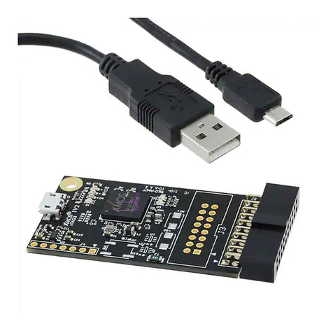
XMOS SliceKit User manual

sliceKIT hardware manual
REV A
Publication Date: 2013/11/6
XMOS © 2013, All Rights Reserved.

sliceKIT hardware manual 2/31
Table of Contents
1 Overview 3
1.1 Introduction .......................................... 3
1.2 sliceKIT system layout .................................... 4
2 Core board 6
2.1 Multiple core boards ..................................... 7
2.2 Setup .............................................. 7
2.3 Power supply .......................................... 7
2.4 Debug .............................................. 7
2.5 XS1-L16 boot .......................................... 8
2.6 xCONNECT Links ....................................... 9
2.7 Reset .............................................. 10
2.8 Clocking ............................................ 10
2.9 Testpoints ........................................... 10
2.10 Slot pinouts .......................................... 13
2.10.1 STAR .......................................... 14
2.10.2 SQUARE ......................................... 16
2.10.3 TRIANGLE ....................................... 18
2.10.4 CIRCLE ......................................... 20
2.10.5 CHAIN ......................................... 22
2.10.6 System services slot signals ............................. 23
3 sliceCARDs and slots 24
4 Designing a sliceCARD 25
4.1 Power .............................................. 25
4.2 Signal I/O ............................................ 25
4.3 sliceCARD form factors .................................... 26
4.4 Connector pinouts ....................................... 27
4.4.1 STAR .......................................... 28
4.4.2 SQUARE ......................................... 29
4.4.3 TRIANGLE ....................................... 30
4.4.4 CIRCLE ......................................... 31
REV A

1 Overview
IN THIS CHAPTER
·Introduction
·sliceKIT system layout
1.1 Introduction
This document covers the hardware design of the sliceKIT Modular Development
System, consisting of the core board, sliceCARDs and xSYS adaptor.
The core board contains a fully pinned out 16-core xCORE multicore microcon-
troller. All GPIOs are connected to four expansion connectors (termed
slots
) which
interface with expansion cards called sliceCARDs that plug into the slots. The core
board also contains all circuitry necessary for operating and debugging the xCORE
system. Multiple sliceKIT core boards can be interconnected to form a multi xCORE
device system with dual 5-bit xCONNECT Links being present between the boards.
REV A

sliceKIT hardware manual 4/31
1.2 sliceKIT system layout
OFF ON
xCONNECT
Link
xSYS
xTAG-2
TILE 0
TILE 0
TILE 1
TILE 1
XS1-L16
XS1-L16
sliceKIT core board
sliceKIT core board
12VDC/1A
12VDC/1A
The diagram above shows an overview of the layout of the core board with slice-
CARDs attached. Each of the four slots has a specific label -
Star
,
Triange
,
Square
,
Circle
printed on the core board silkscreen.
Triangle
and
Circle
sliceCARDs
contain 24 xCORE I/Os, and the
Star
and
Square
sliceCARDs have 20 xCORE
I/Os (usable as GPIO or two 5-wire xCONNECT links). The label denotes which
sliceCARDs are compatible with which core board slots. The sliceCARDs are also
marked with one or more of these labels to identify the slot type(s) they function
correctly with.
REV A

sliceKIT hardware manual 5/31
The final type of connector is on the bottom left of the core board and is marked
with a hollow square symbol with an X through it. This is for connecting multiple
core boards together to form systems of 32 logical cores or more. It is termed the
chain slot.
All slots are 36 pin PCI express style connectors in either socket or edge finger
(plug) types.
Star and Triangle slots are pinned out from Tile 0 of the XS1-L16 xCORE device
and the Circle and Square slots from Tile 1.
REV A

sliceKIT hardware manual 7/31
2.1 Multiple core boards
Additional sliceKIT core boards can be connected to the
Chain
slot on the first
board via the
Square
Slot on the second board, to add extra processing capability
and I/O through extra sliceCARDs. The first board is termed the Master and the
remaining boards are Slaves. When there is only one board, it is the Master.
2.2 Setup
For debugging, an xSYS adaptor board is connected to the
Chain
connector of the
Master board to allow connection of an xTAG-2 which provides a debug link from a
USB host.
The core board is powered by a 12V external power supply.
2.3 Power supply
Power input to the sliceKIT core board is via a standard barrel jack connector. A
standard 12V external power supply should be used to power the board. Each core
board requires its own 12V supply. This input supply is used to generate the main
5V board supply via a DC-DC converter.
The 5V board supply is then fed to all the slot connectors as well as powering the
core board itself. 3V3 and 1V0 supplies are be generated by DC-DC converters
from the 5V main supply.
The supplies are sequenced to ensure the power up sequence is 5V then 3V3 then
1V0. When the 1V0 supply is good, the system is released from reset.
The core board provides 3V3 and 5V at 0.25A each for a total of approximately 2W
per slice.
2.4 Debug
Debug of the system is via the xSYS adapter board connected to the
Chain
connec-
tor.
The JTAG signals are connected as shown below.
REV A

sliceKIT hardware manual 8/31
SOCKET_10
PLUG_00
xTAG-2
TCK
TDI
TDO
TDO
TCK
PRSNT
0
1
TDO
TCK, TMS
TDO
TDI
PRSNT_N
0
1
XS1-L16
TDI
TMS
TMS
TDI
TCK
TMS
Presence detect signals are present on both the
Chain
connector and
Square
slot
connectors to allow detection of a connected board and subsequent automatic
switching of the JTAG chain. In a system of multiple core boards, the Master is the
source of the JTAG chain so the system can only be debugged from the master.
Other boards will see no devices in the JTAG chain.
The use of xSCOPE is covered in the xCONNECT Links section. The xSCOPE
xCONNECT Link can be either enabled or disabled via a switch on the xSYS adapter
board.
2.5 XS1-L16 boot
Master core boards boot from SPI flash, while slave core boards boot from xCON-
NECT link XLB from the next connected core board.
To allow re-use of the SPI boot pins (ports 1A, 1B, 1C, 1D) as signal I/O pins for
the
Star
slot, a latched bus switch is used which connects the xCORE SPI pins to
either the SPI Flash or to the sliceCARD slots. The switch is controlled by X0D42
and X0D43 (P8D6 and P8D7 on Tile 0 - on the
Triangle
slot). Once the device
has booted, X0D43 is used to enable or disable the SPI interface, X0D42 should
Reset
D42 = 0
D43 = X
SPI = EN
Boot
D42 = 0
D43 = X
SPI = EN
Disable
D42 =
D43 = 1
SPI = DIS
Enable
D42 =
D43 = 0
SPI = EN
D42, D43, D0
D1, D10, D11
available
D42, D43 available;
D0, D1, d10, D11
used by SPI
REV A

sliceKIT hardware manual 9/31
then transition from low to high to latch the selection. The SPI selection state is
maintained until the system is reset.
Reset
D42 = 0
D43 = X
SPI = EN
Boot
D42 = 0
D43 = X
SPI = EN
Disable
D42 =
D43 = 1
SPI = DIS
Enable
D42 =
D43 = 0
SPI = EN
D42, D43, D0
D1, D10, D11
available
D42, D43 available;
D0, D1, d10, D11
used by SPI
Once this sequence is completed and the selection has been latched, X0D42 and
X0D43 return to performing their normal functions in the Triangle slot.
If the SPI is not disabled, then SliceCARDs in the
Star
slot may not function as
expected. If there is no sliceCARD in the
Star
slot, then it does not matter whether
the SPI has been disabled or not. Therefore, applications which require runtime
access to the SPI flash should either leave the
Star
slot unpopulated or check to
ensure that the sliceCARD which is in the slot will be unaffected by the operation
of the flash device.
The xTAG-2 system can use the boot mode select signal to force all devices in the
chain (master and slave core boards) to boot from JTAG (don’t boot) for debug
purposes.
If not in this mode, the devices will boot from SPI or xCONNECT Link as appropriate.
2.6 xCONNECT Links
The
Chain
connector contains two 5-bit xCONNECT Links, XLA and XLB, which can
be used to chain sliceKIT core boards together. The links from Tile 0 are connected
REV A

sliceKIT hardware manual 10/31
to the Chain connector and the Star slot. The links from Tile 1 are connected to
the Square slot.
The only complication in this system is use of the xSCOPE 2-bit xCONNECT Link.
This link overlaps a 4 bit port on the Star slot connector so it is not possible to use
this for user I/O at the same time as xSCOPE.
To work around this, a switch is present on the xSYS adapter board to either enable
or disable the xSCOPE xCONNECT Link. When disabled, these pins are disconnected
from the
Chain
connector and are free for use on the
Star
slot. When enabled they
will work as an xCONNECT Link and hence appear on the relevant pins of the
Star
slot.
It is recommended that if a sliceCARD is used in the Star Slot the XSCOPE switch is
off on the xSYS adaptor card to ensure correct operation of the sliceCARD in the
Star slot.
2.7 Reset
The whole system is held in reset until all power supplies are stable, and reset
is connected to all Slice Cards so any circuitry on them can be reset. Reset also
indicates to the sliceCARDs that their power input is stable. The reset from the
xTAG-2 resets the whole system, if required for debugging.
2.8 Clocking
The system clock has two sources: an on-board 25MHz oscillator or the CLK signal
from the Chain connector. The system clock source is selected automatically
according to the presence of signals on the Chain connector.
This means the system clock from a Master core board is fed automatically to all
of the slave core boards so the whole system will operate synchronously.
The system clock is also fed to each of the sliceCARD slots.
2.9 Testpoints
Each xCORE I/O signal is also available on a 0.1” header, next to the slot that it is
connected to. These connections can be used to connect an oscilloscope or logic
analyser, or for interconnection of signals for advanced development work.
The signals are identified on the silkscreen layer of the sliceKIT core board; the
table below lists their relationship to the internal ports.
L16 Pin Slot PCIE Function
X0D0 TRIANGLE B2 P1A0
X0D1 STAR A8 P1B0
CHAIN B10
(continued)
REV A


sliceKIT hardware manual 11/31
L16 Pin Slot PCIE Function
X0D2 STAR B6 P4A0 P8A0 P16A0 P32A20
CHAIN A7
X0D3 STAR B7 P4A1 P8A1 P16A1 P32A21
CHAIN A6
X0D4 STAR B9 P4B0 P8A2 P16A2 P32A22
CHAIN A11
X0D5 STAR B11 P4B1 P8A3 P16A3 P32A23
CHAIN A9
X0D6 STAR A9 P4B2 P8A4 P16A4 P32A24
CHAIN B11
X0D7 STAR A11 P4B3 P8A5 P16A5 P32A25
CHAIN B9
X0D8 STAR A6 P4A2 P8A6 P16A6 P32A26
CHAIN B7
X0D9 STAR A7 P4A3 P8A7 P16A7 P32A27
CHAIN B6
X0D10 STAR B10 P1C0
CHAIN A8
X0D11 TRIANGLE B4 P1D0
X0D12 TRIANGLE A3 P1E0
X0D13 STAR A15 P1F0
CHAIN B15
X0D14 STAR B12 P4C0 P8B0 P16A8 P32A28
CHAIN A13
X0D15 STAR B13 P4C1 P8B1 P16A9 P32A29
CHAIN A12
X0D16 STAR B17 P4D0 P8B2 P16A10
CHAIN A18
X0D17 STAR B18 P4D1 P8B3 P16A11
CHAIN A17
X0D18 STAR A17 P4D2 P8B4 P16A12
CHAIN B18
X0D19 STAR A18 P4D3 P8B5 P16A13
CHAIN B17
X0D20 STAR A12 P4C2 P8B6 P16A14 P32A30
CHAIN B13
X0D21 STAR A13 P4C3 P8B7 P16A15 P32A31
CHAIN B12
X0D22 STAR B15 P1G0
CHAIN A15
X0D23 TRIANGLE A4 P1H0
(continued)
REV A

sliceKIT hardware manual 12/31
L16 Pin Slot PCIE Function
X0D24 TRIANGLE B15 P1I0
X0D25 TRIANGLE A8 P1J0
X0D26 TRIANGLE B6 P4E0 P8C0 P16B0
X0D27 TRIANGLE B7 P4E1 P8C1 P16B1
X0D28 TRIANGLE B9 P4F0 P8C2 P16B2
X0D29 TRIANGLE B11 P4F1 P8C3 P16B3
X0D30 TRIANGLE A9 P4F2 P8C4 P16B4
X0D31 TRIANGLE A11 P4F3 P8C5 P16B5
X0D32 TRIANGLE A6 P4E2 P8C6 P16B6
X0D33 TRIANGLE A7 P4E3 P8C7 P16B7
X0D34 TRIANGLE B10 P1K0
X0D35 TRIANGLE A15 P1L0
X0D36 TRIANGLE B12 P1M0 P8D0 P16B8
X0D37 TRIANGLE B13 P1N0 P8D1 P16B9
X0D38 TRIANGLE B17 P1O0 P8D2 P16B10
X0D39 TRIANGLE B18 P1P0 P8D3 P16B11
X0D40 TRIANGLE A17 P8D4 P16B12
X0D41 TRIANGLE A18 P8D5 P16B13
X0D42 TRIANGLE A12 P8D6 P16B14
X0D43 TRIANGLE A13 P8D7 P16B15
X1D0 CIRCLE B2 P1A0
X1D1 SQUARE A8 P1B0
X1D2 SQUARE B6 P4A0 P8A0 P16A0 P32A20
X1D3 SQUARE B7 P4A1 P8A1 P16A1 P32A21
X1D4 SQUARE B9 P4B0 P8A2 P16A2 P32A22
X1D5 SQUARE B11 P4B1 P8A3 P16A3 P32A23
X1D6 SQUARE A9 P4B2 P8A4 P16A4 P32A24
X1D7 SQUARE A11 P4B3 P8A5 P16A5 P32A25
X1D8 SQUARE A6 P4A2 P8A6 P16A6 P32A26
X1D9 SQUARE A7 P4A3 P8A7 P16A7 P32A27
X1D10 SQUARE B10 P1C0
X1D11 CIRCLE B4 P1D0
X1D12 CIRCLE A3 P1E0
X1D13 SQUARE A15 P1F0
X1D14 SQUARE B12 P4C0 P8B0 P16A8 P32A28
X1D15 SQUARE B13 P4C1 P8B1 P16A9 P32A29
X1D16 SQUARE B17 P4D0 P8B2 P16A10
X1D17 SQUARE B18 P4D1 P8B3 P16A11
X1D18 SQUARE A17 P4D2 P8B4 P16A12
X1D19 SQUARE A18 P4D3 P8B5 P16A13
X1D20 SQUARE A12 P4C2 P8B6 P16A14 P32A30
(continued)
REV A

sliceKIT hardware manual 13/31
L16 Pin Slot PCIE Function
X1D21 SQUARE A13 P4C3 P8B7 P16A15 P32A31
X1D22 SQUARE B15 P1G0
X1D23 CIRCLE A4 P1H0
X1D24 CIRCLE B15 P1I0
X1D25 CIRCLE A8 P1J0
X1D26 CIRCLE B6 P4E0 P8C0 P16B0
X1D27 CIRCLE B7 P4E1 P8C1 P16B1
X1D28 CIRCLE B9 P4F0 P8C2 P16B2
X1D29 CIRCLE B11 P4F1 P8C3 P16B3
X1D30 CIRCLE A9 P4F2 P8C4 P16B4
X1D31 CIRCLE A11 P4F3 P8C5 P16B5
X1D32 CIRCLE A6 P4E2 P8C6 P16B6
X1D33 CIRCLE A7 P4E3 P8C7 P16B7
X1D34 CIRCLE B10 P1K0
X1D35 CIRCLE A15 P1L0
X1D36 CIRCLE B12 P1M0 P8D0 P16B8
X1D37 CIRCLE B13 P1N0 P8D1 P16B9
X1D38 CIRCLE B17 P1O0 P8D2 P16B10
X1D39 CIRCLE B18 P1P0 P8D3 P16B11
2.10 Slot pinouts
The signal assignments for the connectors on the core board and sliceCARDs are
shown in the table below.
REV A

sliceKIT hardware manual 14/31
2.10.1 STAR
PCIE B (TOP) SIGNAL FUNCTION
B1 NC NOT CONNECTED
B2 NC NOT CONNECTED
B3 GND POWER SUPPLY GROUND
B4 NC NOT CONNECTED
B5 3V3 POWER SUPPLY 3.3V
B6 X0D2 P4A0 P8A0 P16A0 P32A20
B7 X0D3 P4A1 P8A1 P16A1 P32A21
B8 GND POWER SUPPLY GROUND
B9 X0D4 P4B0 P8A2 P16A2 P32A22
B10 X0D10 P1C0
B11 X0D3 P4B1 P8A3 P16A3 P32A23
KEY KEY MECHANICAL KEY
B12 X0D14 P4C0 P8B0 P16A8 P32A28
B13 X0D15 P4C1 P8B1 P16A9 P32A29
B14 CLK MAIN SYSTEM CLOCK
B15 X0D22 P1G0
B16 GND POWER SUPPLY GROUND
B17 X0D16 P4D0 P8B2 P16A10
B18 X0D17 P4D1 P8B3 P16A11
REV A

sliceKIT hardware manual 15/31
PCIE A (BOT) SIGNAL FUNCTION
A1 NC NOT CONNECTED
A2 5V POWER SUPPLY 5V
A3 NC NOT CONNECTED
A4 NC NOT CONNECTED
A5 GND POWER SUPPLY GROUND
A6 X0D8 P4A2 P8A6 P16A6 P32A26
A7 X0D9 P4A3 P8A7 P16A7 P32A27
A8 X0D1 P1B0
A9 X0D6 P4B2 P8A4 P16A4 P32A24
A10 GND POWER SUPPLY GROUND
A11 X0D7 P4B3 P8A5 P16A5 P32A25
KEY KEY MECHANICAL KEY
A12 X0D20 P4C2 P8B6 P16A14 P32A30
A13 X0D21 P4C3 P8B7 P16A15 P32A31
A14 GND POWER SUPPLY GROUND
A15 X0D13 P1F0
A16 RST_N SYSTEM RESET (ACTIVE LOW)
A17 X0D18 P4D2 P8B4 P16A12
A18 X0D19 P4D3 P8B5 P16A13
REV A

sliceKIT hardware manual 16/31
2.10.2 SQUARE
PCIE B (TOP) SIGNAL FUNCTION
B1 DEBUG XSYS DEBUG SIGNAL
B2 TCK XSYS TCK SIGNAL
B3 GND POWER SUPPLY GROUND
B4 TDI XSYS TDI SIGNAL
B5 3V3 POWER SUPPLY 3.3V
B6 X1D2 P4A0 P8A0 P16A0 P32A20
B7 X1D3 P4A1 P8A1 P16A1 P32A21
B8 GND POWER SUPPLY GROUND
B9 X1D4 P4B0 P8A2 P16A2 P32A22
B10 X1D10 P1C0
B11 X1D3 P4B1 P8A3 P16A3 P32A23
KEY KEY MECHANICAL KEY
B12 X1D14 P4C0 P8B0 P16A8 P32A28
B13 X1D15 P4C1 P8B1 P16A9 P32A29
B14 CLK MAIN SYSTEM CLOCK
B15 X1D22 P1G0
B16 GND POWER SUPPLY GROUND
B17 X1D16 P4D0 P8B2 P16A10
B18 X1D17 P4D1 P8B3 P16A11
REV A

sliceKIT hardware manual 17/31
PCIE A (BOT) SIGNAL FUNCTION
A1 MSEL XYSY MSEL SIGNAL
A2 5V POWER SUPPLY 5V
A3 TMS XSYS TMS SIGNAL
A4 TDO XSYS TDO SIGNAL
A5 PRSNT SYSTEM PRESENT SIGNAL (ACTIVE LOW)
A6 X1D8 P4A2 P8A6 P16A6 P32A26
A7 X1D9 P4A3 P8A7 P16A7 P32A27
A8 X1D1 P1B0
A9 X1D6 P4B2 P8A4 P16A4 P32A24
A10 GND POWER SUPPLY GROUND
A11 X1D7 P4B3 P8A5 P16A5 P32A25
KEY KEY MECHANICAL KEY
A12 X1D20 P4C2 P8B6 P16A14 P32A30
A13 X1D21 P4C3 P8B7 P16A15 P32A31
A14 GND POWER SUPPLY GROUND
A15 X1D13 P1F0
A16 RST_N SYSTEM RESET (ACTIVE LOW)
A17 X1D18 P4D2 P8B4 P16A12
A18 X1D19 P4D3 P8B5 P16A13
REV A

sliceKIT hardware manual 18/31
2.10.3 TRIANGLE
PCIE B (TOP) SIGNAL FUNCTION
B1 NC NOT CONNECTED
B2 X0D0 P1A0
B3 GND POWER SUPPLY GROUND
B4 X0D11 P1D0
B5 3V3 POWER SUPPLY 3.3V
B6 X0D26 P4E0 P8C0 P16B0
B7 X0D27 P4E1 P8C1 P16B1
B8 GND POWER SUPPLY GROUND
B9 X0D28 P4F0 P8C2 P16B2
B10 X0D34 P1K0
B11 X0D29 P4F1 P8C3 P16B3
KEY KEY MECHANICAL KEY
B12 X0D36 P1M0 P8D0 P16B8
B13 X0D37 P1N0 P8D1 P16B9
B14 CLK MAIN SYSTEM CLOCK
B15 X0D24 P1I0
B16 GND POWER SUPPLY GROUND
B17 X0D38 P1O0 P8D2 P16B10
B18 X0D39 P1P0 P8D3 P16B11
REV A

sliceKIT hardware manual 19/31
PCIE A (BOT) SIGNAL FUNCTION
A1 NC NOT CONNECTED
A2 5V POWER SUPPLY 5V
A3 X0D12 P1E0
A4 X0D23 P1H0
A5 GND POWER SUPPLY GROUND
A6 X0D32 P4E2 P8C6 P16B6
A7 X0D33 P4E3 P8C7 P16B7
A8 X0D25 P1J0
A9 X0D30 P4F2 P8C4 P16B4
A10 GND POWER SUPPLY GROUND
A11 X0D31 P4F3 P8C5 P16B5
KEY KEY MECHANICAL KEY
A12 X0D42 P8D6 P16B14
A13 X0D43 P8D7 P16B15
A14 GND POWER SUPPLY GROUND
A15 X0D35 P1L0
A16 RST_N SYSTEM RESET (ACTIVE LOW)
A17 X0D40 P8D4 P16B12
A18 X0D41 P8D5 P16B13
REV A

sliceKIT hardware manual 20/31
2.10.4 CIRCLE
PCIE B (TOP) SIGNAL FUNCTION
B1 NC NOT CONNECTED
B2 X1D0 P1A0
B3 GND POWER SUPPLY GROUND
B4 X1D11 P1D0
B5 3V3 POWER SUPPLY 3.3V
B6 X1D26 P4E0 P8C0 P16B0
B7 X1D27 P4E1 P8C1 P16B1
B8 GND POWER SUPPLY GROUND
B9 X1D28 P4F0 P8C2 P16B2
B10 X1D34 P1K0
B11 X1D29 P4F1 P8C3 P16B3
KEY KEY MECHANICAL KEY
B12 X1D36 P1M0 P8D0 P16B8
B13 X1D37 P1N0 P8D1 P16B9
B14 CLK MAIN SYSTEM CLOCK
B15 X1D24 P1I0
B16 GND POWER SUPPLY GROUND
B17 X1D38 P1O0 P8D2 P16B10
B18 X1D39 P1P0 P8D3 P16B11
REV A
Table of contents
Other XMOS Computer Hardware manuals

XMOS
XMOS SliceKit GPIO User guide

XMOS
XMOS VocalFusion XVF3510 User manual

XMOS
XMOS XK-XMP-64 User manual

XMOS
XMOS xCORE-Analog sliceKIT User manual

XMOS
XMOS XC-1A User manual

XMOS
XMOS XS1-L2 User manual

XMOS
XMOS XTAG-2 User manual

XMOS
XMOS MultiUART User manual

XMOS
XMOS XS1-L1 User manual

XMOS
XMOS XC-1 User manual
Popular Computer Hardware manuals by other brands

Simplex
Simplex 4001-9813 installation instructions

Renesas
Renesas H8SX series user manual

Sony
Sony PCWA-C150S - Wireless Lan Pc Card troubleshooting guide

Xilinx
Xilinx Virtex-4 QV FPGA manual

NETGEAR
NETGEAR WG511 - Only Wireless Pccard Nic 54MBPS installation guide

Supermicro
Supermicro MBB-CMM-6 user guide