This
manual
is
intend
ed to
se
rve
as
a supplement
to
the
FT-470
Operating
Manual.
Specifications
and
de
tails
of
operation
and
opt
ions are provided
in
the
Operating
Manual, and
are
not
reprint
ed he
rei
n.
Therefore,
this manual
is
not
int
ended
to
serve
as
an
independent
referenc
e,
but
to
be used
in
conjunction
with
the
information
provided
in
the
Operating
Manual.
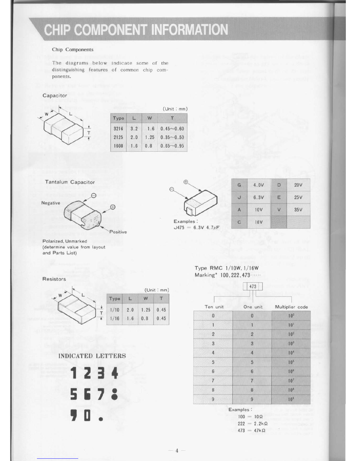
Two
layout
diagrams are
provided
for
each double
-s
id
ed glass-epoxy
circuit
board
in
the
FT
-470. Each
side
of
the board is
identified
by the
type
of
the
majority
of
components installed
on
that
side. In
mo
st
cases one side has
only
c
hip
components, and the
other
has
either
a mixture
of
both c
hip
and lead compo-
nents (trimmers, coils,
electrolytic
capacitors, packaged !Cs,
etc.),
or
leaded components
only.
W
hile
we
believe
the
technical
information
in
this manual
is
correct,
Yaesu
assu
m
es
no
liability
for
damage
that
m3y
occur
as
a r
esu
lt
of
typographi
cal
or
other
e
rrors
that
may be present. Yo
ur
coopera
ti
on
in
pointing
out
any incons
ist
e
nci
es
in
the
technical
informa!ion
would be apprec
iat
ed.
Yaesu Musen reserves the
right
to
make changes
in
the c
ircuitry
of
this
tr
ansce
iv
er,
in
the
inter
es
t
of
technological
improvement,
without
notification
of
the owners.
·f""""""'~~~
.....
..:.-~~~.,..~~~"""~"""""'T"..;..~"':"~~~
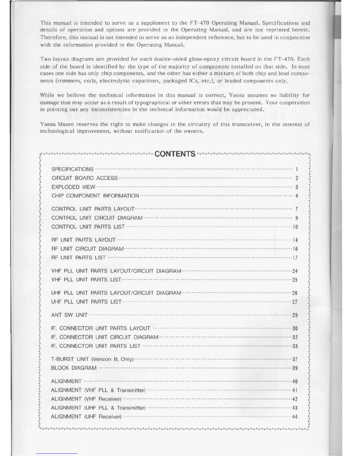
CONTENTS
":"..;..~"':"...:,..~~"'=""...c,.~"t'·""""""""".,..""".,....;..~
.........
~-.-..,:..~~.,....;..
.........
.,..~>
\ '
t f
~
t
t SPECIFICATIONS ·..·················..··..········
..
··········..·······..···················..·
..
···················
..
·..····· 1 f
t CIRCUIT BOARD ACCESS ·········..·······..·..··········....·········....·····......·····
..
·······
..
·······..·..········ 2 t
o)
o)
) EXPLODED VIEW
......................................
·····
.......................................
··......··...........
......
3
~i
(•
(•
i
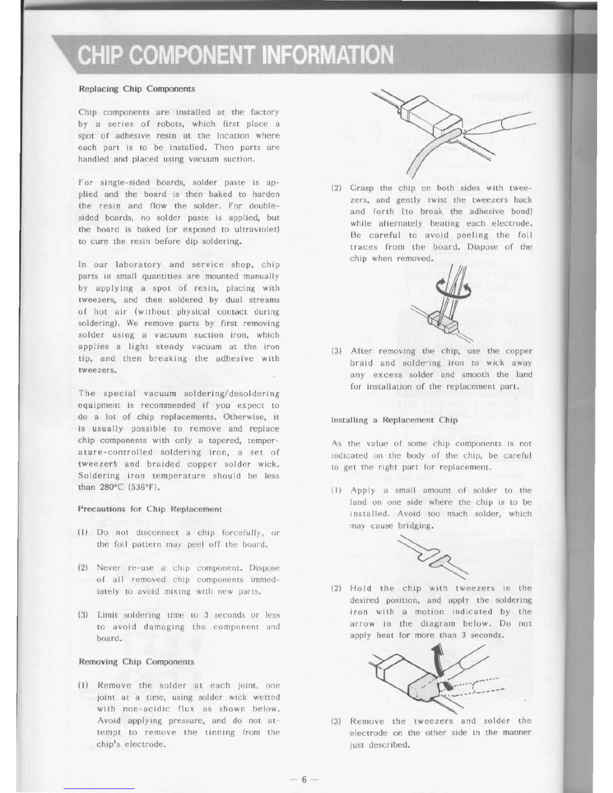
CHIP
COMPONENT INFORMATION
................
..·..·
................
·
......
·
......................
··
..........
··
·..
4
~
~
.
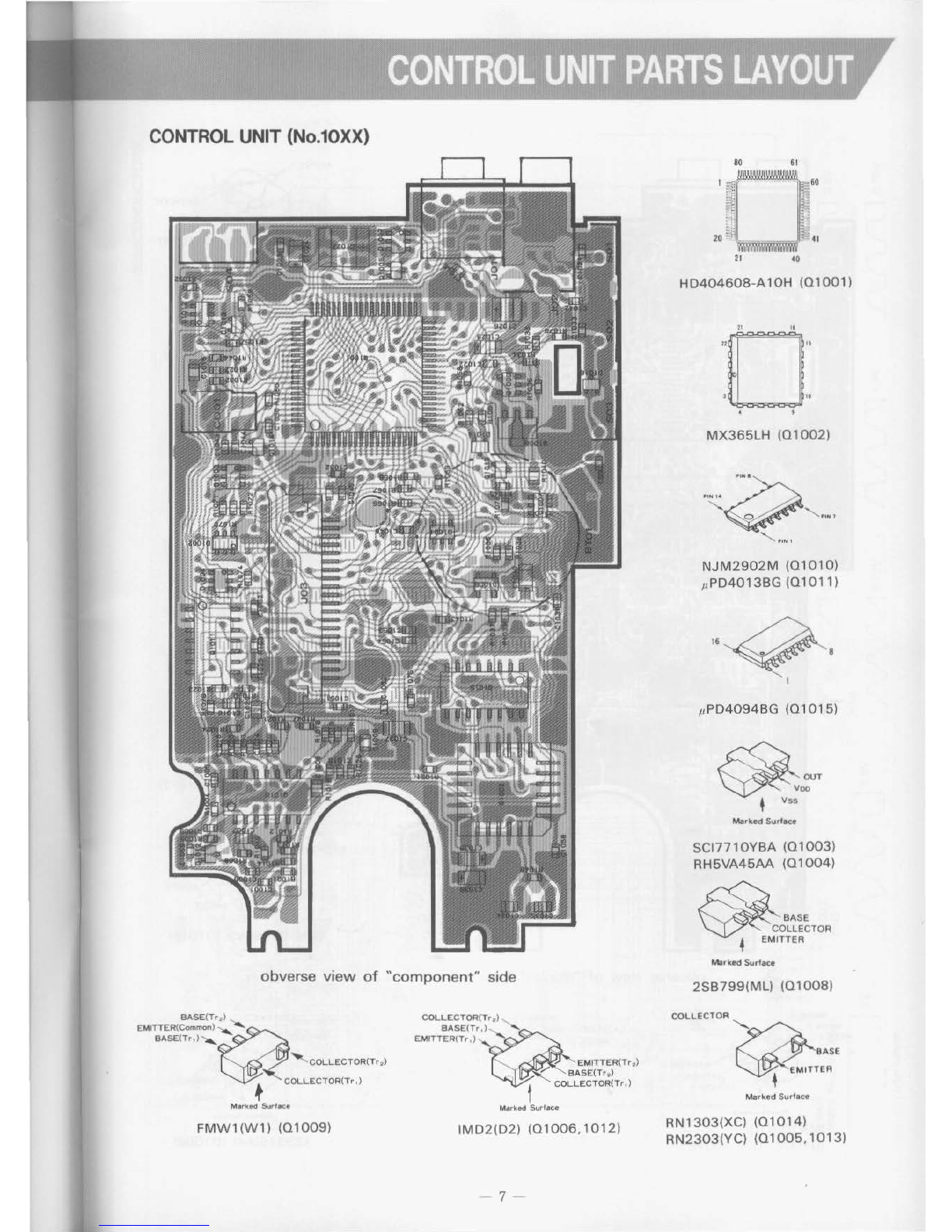
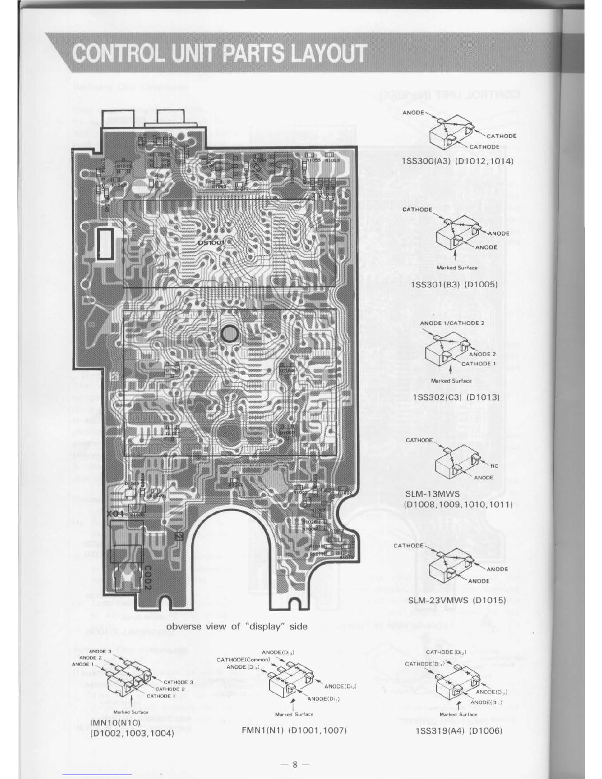
CONTROL UNIT
PARTS
LAYOUT........
.......
...................
........
.......................................
.......
7 i
o)
CONTROL UNIT CIRCUIT DIAGRAM ··················································································· 9 1
•
t
(.
~
CONTROL UNIT
PARTS
LIST
·········
·
············
·······································································
10
i~
t
(.
t t
t
RF
UNIT
PARTS
LAYOUT·..
·······
..··....·..····..·..
··········
..·..····..··....
·······
..
·······
..
····......···
..
········
14
t
~
RF
UNIT CIRCUIT DIAGRAM
........................
·..·..·
......
·
...................
·
....................
·....·
..........
16
~
• •
i~
RF
UNIT
PARTS
LIST ..··········..·....·····..·
..
·············
..
·······..·············
..
······..········
..
·······
..
····..··
17
(.
~. ~.
1 VHF PLL UNIT
PARTS
LAYOUT/CIRCUIT DIAGRAM....·
........
....·......·....
.....................
............
24
~
~·
VHF
PLL UNIT
PARTS
LIST
...................
·..·
..........
·
.............
·....
....................
·
..................
·..
·25
;?
• t
~
UHF
PLL UNIT
PARTS
LAYOUT/CIRCUIT DIAGRAM
...........
.......
...........................................
26
~
• •
j
UHF
PLL UNIT
PARTS
LIST-
...........................................
....
...............................................
27
j
t
(.
o)
(•
(.
o)
ANT SW UNIT
.................................................................................................................
29
IF,
CONNECTOR UNIT PARTS LAYOUT
..............................................................................
30
~.·:
IF,
CONNECTOR UNIT CIRCUIT DIAGRAM·
...............
·
........
·
...............
..
·
..............................
32
(·
~
IF,
CONNECTOR UNIT
PARTS
LIST
....................................................................................
33
i~
~:·:
t~
~
T-BURST UNIT (Version 8, Only)
.......................
·
.....................................................
......
.....
37
i
(.
BLOCK DIAGRAM
.................................................................................................
......
.....
39
~
t •
(.
. ALIGNMENT
..................
·
........
.......
........
·······
........
···
..................
·
...........
······
.........
......
.....
40
;?
?.
<'?
->
ALIGNMENT
(VHF
PLL & Transmitter) ....·....·
..........
·
..................
·....·
..........
·
......
··
........
·.......
·41
·)
~
~:·:.
!<
...
:.·
ALIGNMENT (VHF Receiver)
...................
..........
.....
.....
........
..
......
.
...................
...................
42
ALIGNMENT
(UHF
PLL & Transmitter)·....··......·
........
··..·
..........
·....
................
···....·
.....
........
··
43
o)
o)
j ALIGNMENT
(UHF
Receiver)
..............................................................................................
44
~
"""""'..;..""w~~~..;..~.,..~~~~"':"~~..,...;....,...;...,....;.."':"..;.."':"~~~~~.,....;...,..~..,.w.,..w.,....;..
.....
~-...~~~~~
..........
""'-~..;....,.~~.,....;...,..w~•.,..~~
.....
~~~~~
.....
..,.J