A-EON AMIGAONE X5000 Product manual

CYRUS PLUS MOTHERBOARD
TECHNICAL REFERENCE MANUAL
VERSION 1.1.1 AMIGAONE X5000

16 July 2014 ©A-EON Technology Cyrus Plus Technical Reference Manual 1.1.1 2/36
Issue
Author
Approved
Date
1
James Felix
Marcin Jankowski
16/05/2014
1.1
James Felix
Marcin Jankowski
10/06/2014
1.1.1
Lyle Hazlewood
R.T.Dickinson
16/07/2014
1CONTENTS
1Contents ......................................................................................................................................................... 2
2Introduction.................................................................................................................................................... 7
2.1 Technical Support..................................................................................................................................... 7
2.2 Abbreviations ........................................................................................................................................... 7
3Architecture.................................................................................................................................................... 8
3.1 CPU........................................................................................................................................................... 8
3.1.1 P3041 .............................................................................................................................................. 8
3.1.2 P5020 .............................................................................................................................................. 9
3.1.3 P5040 .............................................................................................................................................. 9
3.2 Main Memory........................................................................................................................................... 9
3.3 Ethernet Phy............................................................................................................................................. 9
3.4 Xena.......................................................................................................................................................... 9
3.5 CPLD ......................................................................................................................................................... 9
3.6 Boot SD Card .......................................................................................................................................... 10
3.7 BIOS ........................................................................................................................................................ 10
4CPU ............................................................................................................................................................... 11
4.1 SerDes Lanes .......................................................................................................................................... 11
4.2 UARTS..................................................................................................................................................... 11
4.3 GPIOs ...................................................................................................................................................... 12
4.4 External Interrupts ................................................................................................................................. 12
4.5 I2C Controller .......................................................................................................................................... 12
4.6 Serial Terminal........................................................................................................................................ 13
5DDR3 DIMMs ................................................................................................................................................ 14
5.1 Size ......................................................................................................................................................... 14
5.2 Speed...................................................................................................................................................... 14
5.3 Serial Presence Detect............................................................................................................................ 14
6XMOS Subsystem.......................................................................................................................................... 15
6.1 Block Diagram......................................................................................................................................... 16
6.2 XENA Connetors ..................................................................................................................................... 17

16 July 2014 ©A-EON Technology Cyrus Plus Technical Reference Manual 1.1.1 3/36
6.3 XMOS Device Type and Clocking ............................................................................................................ 17
6.4 Bootstrapping and Debug ...................................................................................................................... 17
6.5 CPU COMMS........................................................................................................................................... 18
6.6 Xorro Slot................................................................................................................................................ 19
6.7 LEDs ........................................................................................................................................................ 19
6.8 Spare Port Line ....................................................................................................................................... 19
6.9 PCU......................................................................................................................................................... 19
6.10 Haze Xorro Header ............................................................................................................................ 19
7CPLD.............................................................................................................................................................. 20
7.1 CPU COMMS........................................................................................................................................... 20
7.1.1 CPLD XMOS DEBUG Register......................................................................................................... 21
7.1.2 CPLD XMOS JTAG register............................................................................................................. 21
7.1.3 CPLD PCIe register......................................................................................................................... 21
7.1.4 CPLD Build Format ........................................................................................................................ 21
8MCU.............................................................................................................................................................. 22
8.1 Supervisor Interface ............................................................................................................................... 22
8.1.1 Power Button................................................................................................................................ 22
8.1.2 Shut Power Down ......................................................................................................................... 22
8.1.3 Temperatures Readings................................................................................................................ 22
8.1.4 Voltages ........................................................................................................................................ 23
8.1.5 CPU Fan Speed.............................................................................................................................. 24
8.2 Debug Serial Terminal ............................................................................................................................ 24
9Boot .............................................................................................................................................................. 26
9.1 Micro SD card ......................................................................................................................................... 26
9.2 U-Boot .................................................................................................................................................... 26
10 CONNECTOR, JUMPER AND LEDS........................................................................................................... 27
10.1 Switches............................................................................................................................................. 27
10.2 Jumpers ............................................................................................................................................. 27
10.3 LEDs ................................................................................................................................................... 28
10.4 PCIe and PCI Slots .............................................................................................................................. 29
10.5 Xena Connectors................................................................................................................................ 33
10.6 Programming Headers....................................................................................................................... 36
10.6.1 CPLD.............................................................................................................................................. 36
10.6.2 MCU .............................................................................................................................................. 36

16 July 2014 ©A-EON Technology Cyrus Plus Technical Reference Manual 1.1.1 4/36

16 July 2014 ©A-EON Technology Cyrus Plus Technical Reference Manual 1.1.1 5/36
FIGURES
Figure 1: Cyrus Plus Block Diagram......................................................................................................................... 8
Figure 2: XMOS Subsystem Block Diagram ........................................................................................................... 16
Figure 3: XENA connector positions ..................................................................................................................... 17
Figure 4: MCU Debug header ............................................................................................................................... 24
Figure 5: Front Panel LED and switches................................................................................................................ 27
Figure 6: Cyrus Jumpers........................................................................................................................................ 27
Figure 7: Cyrus Plus LEDs ...................................................................................................................................... 28
Figure 8: PCIe and PCI slots................................................................................................................................... 29
Figure 9: Programming Headers........................................................................................................................... 36

16 July 2014 ©A-EON Technology Cyrus Plus Technical Reference Manual 1.1.1 6/36
TABLES
Table 1: Ethernet link speed ................................................................................................................................... 9
Table 2: CPU SerDes Lane Assignments................................................................................................................ 11
Table 3: CPU GPIOs ............................................................................................................................................... 12
Table 4: CPU External interrupts .......................................................................................................................... 12
Table 5: I2C CPU List.............................................................................................................................................. 13
Table 6: SIMM SPD Addresses .............................................................................................................................. 14
Table 7: XMOS CPLD pin connections................................................................................................................... 18
Table 8: XMOS CPLD memory map....................................................................................................................... 18
Table 9: Haze Xorro pinout ................................................................................................................................... 19
Table 10: CPLD Local bus memory map................................................................................................................ 20
Table 11: CPLD register XMOS Debug pin map..................................................................................................... 21
Table 12: CPLD register XMOS JTAG pin map ....................................................................................................... 21
Table 13: CPLD register PCIe signals map ............................................................................................................. 21
Table 14: MCU serial pinout ................................................................................................................................. 24
Table 15: SD boot loader blocks ........................................................................................................................... 26
Table 16: U-Boot critical settings.......................................................................................................................... 26
Table 17: U-Boot Amiga OS boot setting .............................................................................................................. 26
Table 18: Jumpers................................................................................................................................................. 27
Table 19: LEDs....................................................................................................................................................... 28
Table 20: PCIe x16 Slots Pinout ............................................................................................................................ 30
Table 21: PCIe x4 Slots Pinout .............................................................................................................................. 31
Table 22: PCIe x1 Slots Pinout .............................................................................................................................. 31
Table 23: PCI Slots Pinout ..................................................................................................................................... 32
Table 24: Xorro Slot Pinout - A row ...................................................................................................................... 33
Table 25: Xorro Slot Pinout - B row ...................................................................................................................... 34
Table 26: Xorro Slot Signal Descriptions............................................................................................................... 35
Table 27: XTAG Connector Pinout ........................................................................................................................ 35
Table 28: CPLD JTAG Header ................................................................................................................................ 36
Table 29: MCU Programming Header................................................................................................................... 36

16 July 2014 ©A-EON Technology Cyrus Plus Technical Reference Manual 1.1.1 7/36
2INTRODUCTION
The Cyrus Plus motherboard combines a high performance Freescale QorIQ CPU with powerful and flexible I/O
features to deliver the ultimate desktop platform for AmigaOS users.
This manual contains hardware and software reference information to assist with installation, configuration
and low level programming of Cyrus Plus.
2.1 TECHNICAL SUPPORT
For technical support, please contact your reseller.
2.2 ABBREVIATIONS
Acronym
Description
PCIe
PCI Express
PSU
Power Supply Unit
CPU
Central Processing Unit
Hot-Plug
Remove or insert connection/cable whilst power is on
RTC
Real time clock
OD
Open Drain
PU
Pulled-Up
PD
Pulled-Down
RO
Read only
RW
Read write
BCD
Binary-coded decimal
ACPI
Advanced Configuration and Power Interface
SD
Secure Digital
ASCII
American Standard Code for Information Interchange
16 July 2014 ©A-EON Technology Cyrus Plus Technical Reference Manual 1.1.1 8/36
3ARCHITECTURE
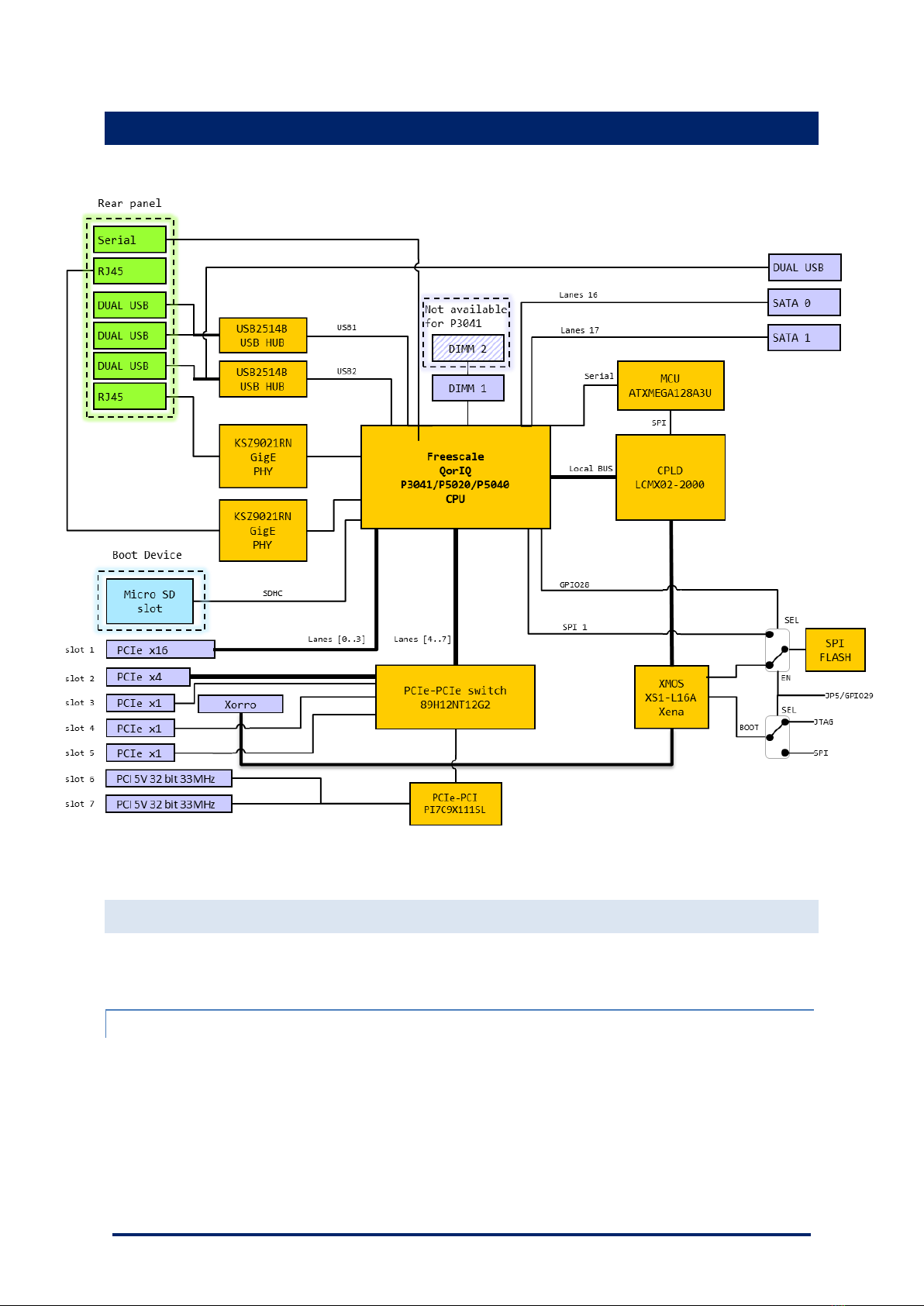
Cyrus Plus’s architecture is shown in Figure 1 below:
Figure 1: Cyrus Plus Block Diagram
3.1 CPU
The CPU on Cyrus Plus is a Freescale QorIQ Power Architecture P series processor. There are 3 options of CPU,
these are the P3041, P5020 and P5040.
3.1.1 P3041
This CPU combines four 1.5 GHz 32-bit e500mc core with a 128KB L2 cache, a single DDR3 memory controller
(1333MT/s) and 18 SerDes channels.
The Power Architecture e500mc cores adhere to most of the Power ISA v2.06 for more information on the
e500mc check the Freescale website.

16 July 2014 ©A-EON Technology Cyrus Plus Technical Reference Manual 1.1.1 9/36
3.1.2 P5020
This CPU combines two 2 GHz 64-bit e5500 core with a 512KB L2 cache, dual DDR3 memory controller
(1333MT/s) and 18 SerDes channels.
The Power Architecture e5500 cores adhere to most of the Power ISA v2.06 for more information on the
e5500 check the Freescale website.
3.1.3 P5040
This CPU combines four 2.2 GHz 64-bit e5500 core with a 512KB L2 cache, dual DDR3 memory controller
(1600MT/s) and 20 SerDes channels.
The Power Architecture e5500 cores adhere to most of the Power ISA v2.06 for more information on the
e5500 check the Freescale website.
3.2 MAIN MEMORY
The P5020 and P5040 variants have two memory controllers, the P3041 variant has one memory controller.
Each CPU memory controller is connected to a standard DDR3 DIMM slot.
For further details, see section 5.
3.3 ETHERNET PHY
The two Micrel KSZ9021RN Gigabit Ethernet PHYs use the RGMII protocol.
The PHYs adaptors use two LEDs to indicate the link speed connection as shown in Table 1. The on LED blinks
when there is activity on the port.
Speed
LED1 (right)
LED2 (left)
1000 link
Off
On
100 link
On
Off
10 link
On
On
Table 1: Ethernet link speed
3.4 XENA
An XMOS XS1-L16A-128 “Software Defined Silicon” (SDS) device is provided to support simple, high
performance I/O.
3.5 CPLD
The CPLD provides glue logic and control registers. It also provides a fast mailbox and data interface between
the CPU and the XENA device.
For further details on the CPLD, see section 7.1 and for the XENA see section 6.5.

16 July 2014 ©A-EON Technology Cyrus Plus Technical Reference Manual 1.1.1 10/36
3.6 BOOT SD CARD
The Cyrus Plus motherboard is booted from a micro SD card. This needs to be fitted in P29 for the Cyrus Plus
motherboard to boot with a valid BIOS in the first 1258 blocks. For more information see section 9.
3.7 BIOS
A micro SD card provided will hold BIOS code.
The BIOS code is maintained by Hyperion.
16 July 2014 ©A-EON Technology Cyrus Plus Technical Reference Manual 1.1.1 11/36
4CPU
This section provides programmer visible details of CPU hardware implementation.
4.1 SERDES LANES
The SerDes lanes are connected as shown in Table 2 below:
Lane
Connection
0
PCIe slot 1 lane 0
1
PCIe slot 1 lane 1
2
PCIe slot 1 lane 2
3
PCIe slot 1 lane 3
4
PCIe switch lane 0
5
PCIe switch lane 1
6
PCIe switch lane 2
7
PCIe switch lane 3
8
Not used.
9
Not used.
10
Not used.
11
Not used.
12
Not used.
13
Not used.
14
Not used.
15
Not used.
16
SATA 0
17
SATA 1
18
Not used
19
Not used
Table 2: CPU SerDes Lane Assignments
Notes:
Lane 18-19 are only available on the P5040.
Unused ports are left un-connected.
4.2 UARTS
The CPU provides two UARTs, one for external RS232 communication and one for MCU supervisor interface.
The UART 0 signals are available on a DB9 connector, P16. This is a 5 wire RS232 interface with RTS and CTS, U-
Boot does not used hardware flow control.
UART 1 is connected to the MCU to get temperature and voltage readings. For further details on the supervisor
interface see section 8.1.

16 July 2014 ©A-EON Technology Cyrus Plus Technical Reference Manual 1.1.1 12/36
4.3 GPIOS
The CPU provides 32 general purpose I/Os (GPIOs) and 14 are used. For details of how these are wired, see
Table 3 below.
GPIO line
Signal Name
Direction
Connection
Notes
GPIO0
Jumper 1
in
CPU_GPIO0
0 = fitted, PU
GPIO1
Jumper 2
in
CPU_GPIO1
0 = fitted, PU
GPIO2
HARD_RESET#
out
CPU_MCU_GPIO0
OD
GPIO3
POWER_OFF#
out
CPU_MCU_GPIO1
OD
GPIO4
CPU_LED
out
CPU LED
PU
GPIO5
HDD_LED
out
HDD ACTIVITY LED
PU
GPIO6
CPLD GPIO 0
in
CPU_CPLD_GPIO0
PU
GPIO7
CPLD GPIO 1
in
CPU_CPLD_GPIO1
PU
GPIO18
CPLD GPIO 2
in
CPU_CPLD_GPIO2
PU
GPIO19
VGA_ BIOS_EN#
in
CPU_GPIO9
0 = fitted, PU
GPIO20
-
in
CPU_GPIO10
PU
GPIO27
RTC_MFP
in
None
PU
GPIO28
EN_XMOS_SPI#
in
EN_XSPI_n
PU 0 = fitted
GPIO29
Program XMOS SPI
out
PROG_XSPI
PD
Table 3: CPU GPIOs
Notes:
A ‘#’ suffix denotes an active-low signal.
4.4 EXTERNAL INTERRUPTS
P5020 External
Interrupt
Connection
Setup
IRQ0#
unused
interrupt input, level sensitive, active low
IRQ1#
Ethernet PHY #2
interrupt input, level sensitive, active low
IRQ2#
XMOS
interrupt input, level sensitive, active low
IRQ3#
Ethernet PHY #1
interrupt input, level sensitive, active low
IRQ4#
CPLD
interrupt input, level sensitive, active low
IRQ5#
MCU
interrupt input, level sensitive, active low
IRQ6#
unused
interrupt input, level sensitive, active low
IRQ7#
unused
interrupt input, level sensitive, active low
IRQ8#
unused
interrupt input, level sensitive, active low
IRQ9#
unused
interrupt input, level sensitive, active low
IRQ10
Jumper 5, JP5
GPIO, input, PU
IRQ11
XMOS SPI data steering mux
GPIO, output, PD
Table 4: CPU External interrupts
4.5 I2C CONTROLLER

16 July 2014 ©A-EON Technology Cyrus Plus Technical Reference Manual 1.1.1 13/36
The CPU has 4 I2C controllers the use of each controller is shown below in Table 5.
I2C BUS
Devices attached
1
NXID and MAC address
2
DDR3 DIMMS
3
SMBUS for PCIe devices
4
RTC
Table 5: I2C CPU List
4.6 SERIAL TERMINAL
For serial communications, on a PC it is recommended to use TeraTerm. The serial port control must be
configured as follows:
▪115200 Baud
▪8 bit data
▪No Parity
▪1 Stop bit
▪No Flow Control

16 July 2014 ©A-EON Technology Cyrus Plus Technical Reference Manual 1.1.1 14/36
5DDR3 DIMMS
Cyrus Plus uses standard 1.5V DDR3 DIMMs, 1 socket for P3041 and 2 sockets for P5020/P5040.
The board has been qualified with unbuffered non-ECC DIMMs. For the latest information on recommended
DIMM module types, please contact your reseller.
It is recommended to use DIMMs in matched pairs.
5.1 SIZE
The total physical maximum size of memory that the memory controllers can address is 64GB, however the
practical memory size limit will depend on software.
5.2 SPEED
The maximum speed supported by the memory controllers is DDR3-1333 for the P3041 and P5020 variants
and DDR3-1600 for the P5040 variant. Faster memory may be fitted but this speed limit will apply.
5.3 SERIAL PRESENCE DETECT
The Serial Presence Detect (SPD) addresses of the 2 DIMM sockets is are as follows:
Socket
SA2
SA1
SA0
Address
DIMM1
0
0
1
0x51
DIMM2
0
1
0
0x52
Table 6: SIMM SPD Addresses

16 July 2014 ©A-EON Technology Cyrus Plus Technical Reference Manual 1.1.1 15/36
6XMOS SUBSYSTEM
Cyrus Plus includes direct support for XMOS “SDS” (Software Defined Silicon) technology. A dedicated XMOS
device, designated “Xena” here, is provided on-board.
Xena is connected to both the main CPU and a custom expansion slot (“Xorro”), which is mechanically aligned
with a conventional PCI Express x1 slot.
Xorro expansion cards may be enhanced by adding connectivity to the PCI Express bus. Alternatively, if the
Xorro slot is not required, the PCI Express slot connector can be used for conventional PCI Express x1 add-in
cards.
This section provides essential details of Cyrus Plus’s XMOS subsystem, and should be read in conjunction with
relevant XMOS documentation.

16 July 2014 ©A-EON Technology Cyrus Plus Technical Reference Manual 1.1.1 16/36
6.1 BLOCK DIAGRAM
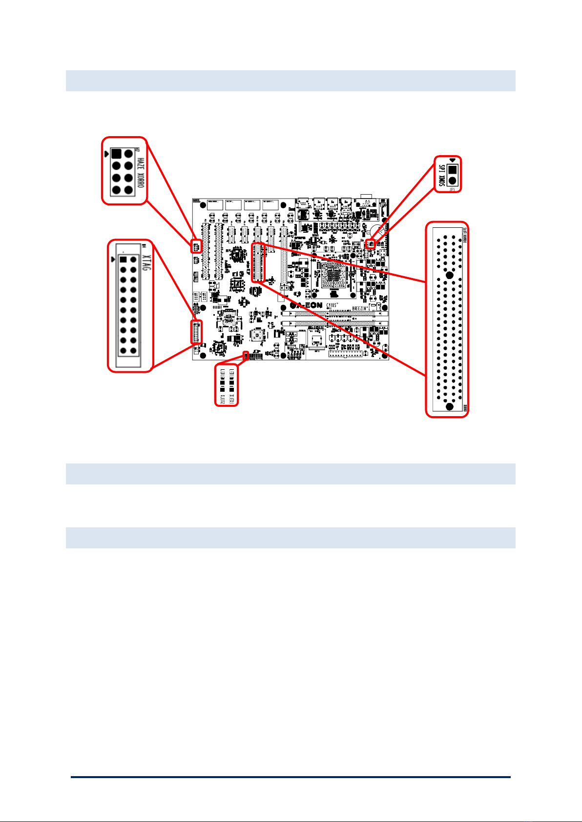
Figure 2 shows how Xena is connected to the main processor, the CPLD, the XTAG debug header and the Xorro
slot.
Figure 2: XMOS Subsystem Block Diagram
16 July 2014 ©A-EON Technology Cyrus Plus Technical Reference Manual 1.1.1 17/36
6.2 XENA CONNECTORS
The XENA connectors are displayed below in Figure 3.
Figure 3: XENA connector positions
6.3 XMOS DEVICE TYPE AND CLOCKING
Xena is a 500MHz, dual-core XS1-L16A (formerly XS1-L2), in a 124-pin QFN package. It is clocked from a 25MHz
oscillator, and its PLL is configured for x20 operation i.e. a core clock speed of 500MHz.
6.4 BOOTSTRAPPING AND DEBUG
Bootstrapping and debug of Xena is accomplished via its reset, JTAG and debug signals. These are connected to
the CPLD, and may be controlled and sampled via the CPU local bus registers that are implemented within it.
For details of these, see section 7.
Normally, software running on the main CPU will only see the Xena chip on this interface. If a Xorro card is
fitted in the slot, and this asserts the slot PRESENT# signal, the CPLD will route the JTAG chain through the
Xorro card, so that any devices on it will appear before Xena (Xorro’s TDO connects to Xena’s TDI).
Xena’s control and debug signals are also connected to a header to allow the use of an XMOS XTAG debugger.
If one is connected, the CPLD will float most of its pins, allowing the XTAG to take over. It will, however, still
provide automatic routing of the TDI/TDO signal chain through a Xorro card, if required, so that the XTAG can
control both Xena and Xorro together.
Haze Xorro
connector
XTAG header
Xorroslot
XMOS LEDs
JP5
SPI XMOS Enable

16 July 2014 ©A-EON Technology Cyrus Plus Technical Reference Manual 1.1.1 18/36
The addition for Cyrus Plus is for an SPI option to boot for the Xena. The SPI device can be programmed via the
CPU when PROG_XSPI (GPIO28) is driven low. This allows for the Xena to be booted at startup without any
need for JTAG programming.
6.5 CPU COMMS
As shown in Figure 2, a number of ports from Xcore 1 are connected to the CPU via the CPLD via a mailbox
interface with a shared dual port RAM. An interrupt is generated when the CPU has written data to the RAM
for the Xena to read data.
Signal
Description
I/O
Xena pin
DATA[0..15]
16 bit data
bidirectional
XS1_PORT_16A
CLK
Bus clock/strobe
output
XS1_PORT_1A
WE#
Write Enable
output
XS1_PORT_1B
RE#
Read Enable
output
XS1_PORT_1C
DI
Data/Index, Data=1 index=0
output
XS1_PORT_1D
IRQ#
Interrupt
input
XS1_PORT_1F
Table 7: XMOS CPLD pin connections
The intention is that a thread on Xcore 1 should be programmed for the mailbox protocol using the pin
assignment in Table 7. The protocol uses indirect addressing in that the address of the area of the memory to
be accessed is first written to the index register (using DI low to select the index register), then reading or
writing the data with DI driven high. Note that the index register will auto increment when reading or writing
to the RAM. When finished writing data to RAM the code should write to the MBX2C register to generate an
interrupt to the CPU. Example code for this will be provided.
The CPU communications to the Xena is similar to the CPLD to Xena, but the index or data registers are directly
memory mapped. The index address is 0x0 and the data address is 0x8000. For example to read the SIG1
value, from the CPU you write 0x0 at address 0x0 and then read the data in 0x8000.
The memory map for Xena to the CPLD is shown below in Table 8.
Address (hex)
Register name
Description
Read/Write
0x0000
SIG1
signature value 1 (0xDEAD)
RO
0x0001
SIG2
signature value 2 (0xBEEF)
RO
0x0002
HWREV
Hardware revision
RO
0x0005
MBC2X
CPU to XMOS mailbox
RW
0x0006
MBX2C
XMOS to CPU mailbox
RO
0x8000-0x8FFF
RAM
Dual port RAM , 16 bits wide, 4kbytes
RW
0x0030
XSCR1
XMOS Scratch register
RW
0x0031
XSCR2
XMOS Scratch register
RW
Table 8: XMOS CPLD memory map

16 July 2014 ©A-EON Technology Cyrus Plus Technical Reference Manual 1.1.1 19/36
6.6 XORRO SLOT
The Xorro slot connector is physically a PCI Express x8 (98 pin) card edge connector. Xorro cards are not
compatible with PCI Express x8 cards.
The pinout of the Xorro slot connector is provided in section 10.5, together with signal descriptions.
6.7 LEDS
A pair of simple LEDs is provided for diagnostic purposes. These are connected to Xcore 0 (port P1K) and Xcore
1 (port P1E), and are illuminated when driven low.
6.8 SPARE PORT LINE
The spare port line (Xcore 0 port P1L) is connected to the CPLD. Its use is reserved and it should be tri-stated.
6.9 PCU
Xena’s PCU (Power Control Unit) is not used.
6.10 HAZE XORRO HEADER
There is an additional header to the Xena to allow for direct connection between the Xena and CPU via the
serial port. The pin out of the Haze Xorro connector, H7 is shown in Table 9.
Pin
Signal
Signal
Pin
1
CPU RX0
X0D1 (P1B0)
2
3
CPU RX0
X0D10 (P1C0)
4
5
CPU TX0
X0D11 (P1D0)
6
7
CPU TX0
X0D12 (P1E0)
8
Table 9: Haze Xorro pinout
Warning: When using the Haze Xorro header make sure that you have configured the Xena IOs so that it is
not driving outputs onto the CPU output signals.

16 July 2014 ©A-EON Technology Cyrus Plus Technical Reference Manual 1.1.1 20/36
7CPLD
The CPLD is connect to the CPU via the local bus and allows for the high speed interface between the CPU and
the XMOS. There are other read only registers which include the CPU fan speed.
7.1 CPU COMMS
The interface for the CPU to the CPLD is similar to the XMOS mail box, the address of the register to be
accessed should first be written to the index register at address (0x0). The data can then be read and written
using the data address (0x8000). For example to check the speed of the CPU fan TACHO you would write 0x10
into address 0x0, then read data from address 0x8000.
For more details on the Xena link protocol referrer to section 6.5.
The memory map for the CPU to the CPLD is shown below in Table 10.
Address (hex)
Register name
Description
Read/Write
0x0000
SIG1
signature value 1 (0xDEAD)
RO
0x0001
SIG2
signature value 2 (0xBEEF)
RO
0x0002
HWREV
Hardware revision
RO
0x0004
IA_LBALIVE
Local bus is alive returns 0x1
RO
0x0005
MBC2X
CPU to XMOS mailbox
RW
0x0006
MBX2C
XMOS to CPU mailbox
RO
0x000C
XDEBUG
XMOS Control see Table 11 for pin assignments
-
0x000D
XJTAG
XMOS JTAG pins see Table 12 for pin assignments
-
0x0010
FAN_TACHO1
Fan speed in Revolution per seconds
RO
0x0011
VID_CA_CB2
Core voltage value VID value
RO
0x0012
VID_PL2
Platform voltage VID value
RO
0x0013
PEX_SIG
PCIe wake and present signals
RO
0x0018
-
Reserved for internal use
-
0x0019
-
Reserved for internal use
-
0x001A
-
Reserved for internal use
-
0x0020
ETH2STATE
Number of Ethernet PHY fitted, [0x1=2 0x0=1]
RO
0x0021
DATE_LB
CPLD build date lower byte, see 7.1.4 for build format
RO
0x0022
DATE_UB
CPLD build date upper byte, see 7.1.4 for build format
RO
0x0023
TIME_LB
CPLD build time lower byte, see 7.1.4 for build format
RO
0x0024
TIME_UB
CPLD build time upper byte, see 7.1.4 for build format
RO
0x0030
SCR1
Scratch register
RW
0x0031
SCR2
Scratch register
RW
0x8000
RAM
Dual port RAM base address , 16 bits wide, 4kbytes
RW
Table 10: CPLD Local bus memory map
Notes:
1. The FAN_TACHO signal should be read multiple times to get rid of metastability.
2. VID values are relevant to P5040 boards only.
Table of contents


