Actel ProASIC3/E User manual

ActelCorporation,Mountain View,CA94043-4655
© 2006 Actel Corporation. All rights reserved.
Printed in the United States of America
Part Number: 50200048-2
Release: April 2009
No part of this document may be copied or reproduced in any form or by any means without prior written
consent of Actel.
Actel makes no warranties with respect to this documentation and disclaims any implied warranties of
merchantability or fitness for a particular purpose. Information in this document is subject to change
without notice. Actel assumes no responsibility for any errors that may appear in this document.
This document contains confidential proprietary information that is not to be disclosed to any
unauthorized person without prior written consent of Actel Corporation.
Trademarks
Actel and the Actel logo are registered trademarks of Actel Corporation.
Adobe and Acrobat Reader are registered trademarks of Adobe Systems, Inc.
All other products or brand names mentioned are trademarks or registered trademarks of their respective
holders.

ProASIC3/E Starter Kit User’s Guide and Tutorial 3
Table of Contents
Introduction . . . . . . . . . . . . . . . . . . . . . . . . . . . . . . . . . . . . 5
Document Contents . . . . . . . . . . . . . . . . . . . . . . . . . . . . . . . . . . . . . . . . . 5
Document Assumptions . . . . . . . . . . . . . . . . . . . . . . . . . . . . . . . . . . . . . . . 5
1 Contents and System Requirements . . . . . . . . . . . . . . . . . . . . . . . 7
2 Hardware Components . . . . . . . . . . . . . . . . . . . . . . . . . . . . . . 9
ProASIC3/E Evaluation Board . . . . . . . . . . . . . . . . . . . . . . . . . . . . . . . . . . . . 9
Detailed Board Description and Usage . . . . . . . . . . . . . . . . . . . . . . . . . . . . . . . . 9
PLL Parts/Usage on ProASIC3 . . . . . . . . . . . . . . . . . . . . . . . . . . . . . . . . . . 11
Power Supplies . . . . . . . . . . . . . . . . . . . . . . . . . . . . . . . . . . . . . . . . . . . 11
Programming the A3PE-A3P-EVAL-BRD1 with a FlashPro3 . . . . . . . . . . . . . . . . . . 15
Clock Circuits . . . . . . . . . . . . . . . . . . . . . . . . . . . . . . . . . . . . . . . . . . . 17
LED Device Connections . . . . . . . . . . . . . . . . . . . . . . . . . . . . . . . . . . . . . 17
Switches Device Connections . . . . . . . . . . . . . . . . . . . . . . . . . . . . . . . . . . . . 18
FPGA – LCD Interface . . . . . . . . . . . . . . . . . . . . . . . . . . . . . . . . . . . . . . 19
LCD Power Supply Circuit . . . . . . . . . . . . . . . . . . . . . . . . . . . . . . . . . . . . . 20
LVDS Channels . . . . . . . . . . . . . . . . . . . . . . . . . . . . . . . . . . . . . . . . . . 20
3 Setup and Self Test . . . . . . . . . . . . . . . . . . . . . . . . . . . . . . . . 23
Software Installation . . . . . . . . . . . . . . . . . . . . . . . . . . . . . . . . . . . . . . . . 23
Hardware Installation . . . . . . . . . . . . . . . . . . . . . . . . . . . . . . . . . . . . . . . . 23
Testing the Evaluation Board . . . . . . . . . . . . . . . . . . . . . . . . . . . . . . . . . . . . 23
Programming the Test File . . . . . . . . . . . . . . . . . . . . . . . . . . . . . . . . . . . . . 23
4 Description of Test Design . . . . . . . . . . . . . . . . . . . . . . . . . . . . 25
5 LVDS Signal Evaluation . . . . . . . . . . . . . . . . . . . . . . . . . . . . . 29
Introduction . . . . . . . . . . . . . . . . . . . . . . . . . . . . . . . . . . . . . . . . . . . . . 29
Test Setup . . . . . . . . . . . . . . . . . . . . . . . . . . . . . . . . . . . . . . . . . . . . . . 29
Measurement Results . . . . . . . . . . . . . . . . . . . . . . . . . . . . . . . . . . . . . . . . 30
6 Actel VHDL ProASIC3/E Design Flow . . . . . . . . . . . . . . . . . . . . . 31
Design Entry . . . . . . . . . . . . . . . . . . . . . . . . . . . . . . . . . . . . . . . . . . . . 32
Design Implementation . . . . . . . . . . . . . . . . . . . . . . . . . . . . . . . . . . . . . . . 33
Programming . . . . . . . . . . . . . . . . . . . . . . . . . . . . . . . . . . . . . . . . . . . . 33
System Verification . . . . . . . . . . . . . . . . . . . . . . . . . . . . . . . . . . . . . . . . . 33
7 Quick Start Tutorial . . . . . . . . . . . . . . . . . . . . . . . . . . . . . . . . 35
Step 1 – Create a New Project . . . . . . . . . . . . . . . . . . . . . . . . . . . . . . . . . . . 35
Step 2 – Perform Pre-Synthesis Simulation . . . . . . . . . . . . . . . . . . . . . . . . . . . . 41
Step 3 – Synthesize the Design in Synplify . . . . . . . . . . . . . . . . . . . . . . . . . . . . . 49
Step 4 – Perform Post-Synthesis Simulation . . . . . . . . . . . . . . . . . . . . . . . . . . . . 51

Table of Contents
4ProASIC3/E Starter Kit User’s Guide and Tutorial
Step 5 – Implement the Design with Designer . . . . . . . . . . . . . . . . . . . . . . . . . . . 52
Step 6 – Perform Timing Simulation with Back-Annotated Timing . . . . . . . . . . . . . . . . 57
Step 7 – Generate the Programming File . . . . . . . . . . . . . . . . . . . . . . . . . . . . . . 58
Step 8 – Program the Device . . . . . . . . . . . . . . . . . . . . . . . . . . . . . . . . . . . . 58
8 Test Procedures for Board Testing . . . . . . . . . . . . . . . . . . . . . . . . 67
Overview . . . . . . . . . . . . . . . . . . . . . . . . . . . . . . . . . . . . . . . . . . . . . . 67
Equipment Required . . . . . . . . . . . . . . . . . . . . . . . . . . . . . . . . . . . . . . . . 67
Test Procedure for the A3PE-A3P-EVAL-BRD1 . . . . . . . . . . . . . . . . . . . . . . . . 67
A PQ208 Package Connections for A3PE600 and A3P250 Devices . . . . . . . . 71
208-Pin PQFP . . . . . . . . . . . . . . . . . . . . . . . . . . . . . . . . . . . . . . . . . . . 72
B Board Schematics . . . . . . . . . . . . . . . . . . . . . . . . . . . . . . . . . 81
Top-Level View . . . . . . . . . . . . . . . . . . . . . . . . . . . . . . . . . . . . . . . . . . . 81
ProASIC3 Schematics . . . . . . . . . . . . . . . . . . . . . . . . . . . . . . . . . . . . . . . 81
C Signal Layers . . . . . . . . . . . . . . . . . . . . . . . . . . . . . . . . . . . 93
D Product Support . . . . . . . . . . . . . . . . . . . . . . . . . . . . . . . . . 101
Customer Service . . . . . . . . . . . . . . . . . . . . . . . . . . . . . . . . . . . . . . . . . 101
Actel Customer Technical Support Center . . . . . . . . . . . . . . . . . . . . . . . . . . . . 101
Actel Technical Support . . . . . . . . . . . . . . . . . . . . . . . . . . . . . . . . . . . . . 101
Website . . . . . . . . . . . . . . . . . . . . . . . . . . . . . . . . . . . . . . . . . . . . . . 101
Contacting the Customer Technical Support Center . . . . . . . . . . . . . . . . . . . . . . . 101
Index . . . . . . . . . . . . . . . . . . . . . . . . . . . . . . . . . . . . . . 103

ProASIC3/E Starter Kit User’s Guide and Tutorial 5
Introduction
Thank you for purchasing the Actel ProASIC3/E Starter Kit.
This guide provides the information required to easily evaluate the ProASIC3/E devices.
Document Contents
Chapter 1 – “Contents and System Requirements” describes the contents of the ProASIC3/E Starter Kit.
Chapter 2 – “HardwareComponents”describesthe componentsof the ProASIC3/E Evaluation Board.
Chapter3 –“Setupand SelfTest” describeshow to setup theProASIC3/E Evaluation Board and how to perform a self
test.
Chapter 4 – “Description of Test Design” describes the existing design on the ProASIC3/E Evaluation Board.
Chapter 5 – “LVDS Signal Evaluation” explains test setup and design, reports the measurements performed on the
board, and makes recommendations to increase the LVDS signal quality in order to meet the performance criteria.
Chapter 6 – “Actel VHDL ProASIC3/E Design Flow” introduces the design flow for VHDL using the Actel Libero®
Integrated Design Environment (IDE) suite.
Chapter 7 – “Quick Start Tutorial” illustrates a VHDL design for a ProASIC3/E starter kit board.
Chapter 8– “Test Procedures for Board Testing” details the test procedure to be carried out at the Actel designated
manufacturer's testing facility on the ProASIC3/E Evaluation Board with silkscreen labeling A3PE-A3P-EVAL-BRD-
1REV3.
Appendix A –“PQ208 Package Connections for A3PE600 and A3P250 Devices” provides a table listing the board
connections.
Appendix B – “BoardSchematics”provides illustrations ofthe ProASIC3/E Evaluation Board.
Appendix C – “Signal Layers” provides illustrations for the six signal layers of the Evaluation Board.
Appendix D– “ProductSupport” describes Actel support services.
Document Assumptions
This user’s guide assumes:
• You intend to use Actel Libero IDE software.
• You have installed and are familiar with Actel Libero IDE v6.2 SP1 or later software.
• You are familiar with VHDL.
• You are familiar with PCs and Windows operating systems.


ProASIC3/E Starter Kit User’s Guide and Tutorial 7
1
Contents and System Requirements
This chapter details the contents of the ProASIC3/E Starter Kit and lists the power supply and software system
requirements.
Starter Kit Contents
The starter kit includes the following:
• ProsASIC3/E Evaluation Board
• Libero IDE Gold
• FlashPro3
•TheProASIC3/E Starter Kit User’s Guide & Tutorial
• CD with design examples
• Switching brick power supply (rated from 110 V to 240 V AC) from 50 Hz to 60 Hz input, providing 9 V DC output
at up to 2 A, part number DTS090220U-P5P-SZ from CUI INC
For the CD contents, review the ReadMe.doc file at the top level of the CD.


ProASIC3/E Starter Kit User’s Guide and Tutorial 9
2
Hardware Components
This chapter describes the hardware components of the ProASIC3/E Evaluation Board.
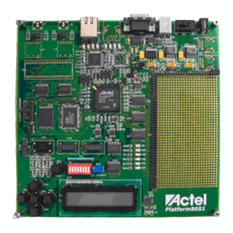
ProASIC3/E Evaluation Board
Figure 2-1 on page 10 illustrates a top-level view of the ProASIC3/E Evaluation Board.
The ProASIC3/E Evaluation Board consists of the following:
• Wall mount power supply connector, with switch and LED indicator
• Switches to select from among 1.5 V, 1.8 V, 2.5 V, and 3.3 V – I/O voltages on banks 4 and 5 (southern side)
• 10-pin 0.1 inch pitch programming connector compatible with Altera connections
• 40 MHz oscillator and two independent manual clock options for global reset and pulse
• Eight LEDs (driven by outputs from the device)
• Jumpers (allow disconnection of all external circuitry from the FPGA)
• Two monostable pulse generator switches ("global" and "reset")
• Four switches (provide input to the device)
• Two hex switches to provide four inputs each to the FPGA, and which are set to a user-switchable hexadecimal input
value
• Large LCD alphanumeric display to facilitate detailed message outputs from the FPGA application
For further information, refer to the following appendices:
Appendix A – “PQ208 Package Connections for A3PE600 and A3P250 Devices” on page 71.
Appendix B – “Board Schematics” on page 81.
Detailed Board Description and Usage
The ProASIC3 Starter kit board has various advanced features that are covered in later sections of this chapter. It will be
noted that the Advanced Prototyping Starter Kit has a socket on the board into which an end user may place any
ProASIC3 device, as all devices in both the ProASIC3 and ProASIC3E families are available in the PQ208 package.
The EVAL kit version can be identified as the one that has the FPGA soldered directly to the board.
A block diagram of the ProASIC3 Starter kit board is shown in Figure 2-1 on page 10 and will facilitate understanding
of the more detailed schematics shown in this tutorial in the appendix, “Board Schematics” on page 81.

Hardware Components
10 ProASIC3/E Starter Kit User’s Guide and Tutorial
Figure 2-1. ProASIC3/E Evaluation Board: Top-Level View
Full schematics areavailable on the Starter Kit Tutorial CD that is supplied with the Starter Kit. The schematics are also
available for download from the Actel website. The electronic versions of the dedicated schematics can naturally be
enlarged to a far greater degree than can be shown in the printed version of this manual or even in the electronic version
of this manual, hence the interested reader is referred to the dedicated schematics to see the appropriate level of detail.

PLL Parts/Usage on ProASIC3
ProASIC3/E Starter Kit User’s Guide and Tutorial 11
PLL Parts/Usage on ProASIC3
Instructions for PLL Activation on ProASIC3 Starter Kit Board
In order to use the PLLs on the ProASIC3 starter kit board, power must be applied to their respective analog supply
rails. For the west side PLL, known as PLF, the VCCPLF line must be connected to VCC, which is held at 1.5 V. The
same is true for VCCPLC of the PLL on the east side, known as PLC. In addition, the VCOMPLF and VCOMPLC lines
must be connected to ground. We do not connect these voltages by default on the board for three reasons:
1. The PLC analog voltagerails are not available on A3P devices, only on A3PE in the PQ208 package. Only the west
sidePLL,namely PLF, isavailableon A3PdevicesinPQ208. InA3P devices,the pinsareusedas generalI/Os. The
same board is used for A3PE and A3P devices.
2. We want to demonstrate the lowest possible power consumption for the part. Perpetually powering the PLL lines
would not achieve that.
3. It is easy to connect the appropriate pins together when desired. That is why we make the pins available on the
headers.
A variety of valid connections are possible. Two examples are as follows:
1. For PLF, connect pin 27 (VCCPLF) to pin 36 (VCC), and pin 25 (VCOMPLF) to pin 17 (GND).
2. For PLC, (A3PE only) connect pin 131 (VCCPLC) to pin 142 (VCC), and pin 133 (VCOMPLC) to pin 141 (GND).
To facilitate end users, we will be supplying jumper wires with selected production versions of the kit to allow end users
to quickly connect and disconnect these voltage supply rails. If a user has lost the jumper wires or has a production kit
without jumper wires, it is a simple matter of solderingshort insulated connecting wire to the appropriate header pins on
the J14A and J14C headers.
Power Supplies
A 9 V power supply is provided with the kit (Figure 2-2). There are many power supply components in the starter kit
board to illustrate the many ways that differing voltage banks may be supported with ProASIC3 and ProASIC3E

Hardware Components
12 ProASIC3/E Starter Kit User’s Guide and Tutorial
technology. These voltage banks are not all required for general use of ProASIC3 silicon. They are provided purely for
illustrative purposes.
Figure 2-2. Power Supply Block Diagram
To use the ProASIC3/E Evaluation boardwith a wall mount power supply, use the switching brick power supply that is
provided with the kit.
The external +9 V positive center power supply provided to the board via connector J16 goes to a voltage regulator chip
U11 on the evaluation board. As soon as the external voltage is connected to the board, the red power applied LED (the
only red LED on the board) D19 illuminates to indicate that an external supply has been connected to the board. As
soon as switch SW11 is moved to the ON position (to the right, as labeled on the board “OFF/ON”), the disabling
ground signal is removed from pin 7 of U11 and the regulator begins to provide power at its output.
The U11 switching voltage regulator provides a dedicated 3.3 V supply at its output. The board’s 3.3 V supply is used for
feeding separate regulators that deliver 1.5 V (via U15), 1.8 V (via U12) and 2.5 V (via U15). The 1.5 V is required for
the core voltage of the ProASIC3 family, and the 2.5 V is required for demonstrating LVDS extended I/O bank
capability.
The presence of these voltages is indicated by four green LEDs (D13, D9, D10, and D11 respectively) illuminating at
the top right of the board. Each LED is labeled with the voltage it represents and its component identifier. All four
voltages are selectable on the I/O banks 4 and 5 (the two southernmost banks on a ProASIC3E device).
Note: Only ProASIC3E devices have 8 I/O banks. ProASIC3 devices have four I/O banks—one per side of the PQ208
package.]
The 3.3 V supply is also used for optionally providing the VPUMP programming voltage. This VPUMP voltage may be
provided to the chip during programming by applying a FlashPro3 programmer to the J1 interface and selecting VPUMP
from the FlashPro v3.3 (or later) programming software. VPUMP voltage may also be provided directly to the chip from
the board.
Simply leave the JP48 jumper in place toapply the 3.3 V supply to the VPUMP pin (106 of the PQ208 packaged FPGA).
Note that if bothFlashPro3 and the board are selected to provide VPUMP, then it is the connection on the board thatwill
override, as FlashPro3 will detect that a voltage is available, issue an information message in the programming software,
and then move the VPUMP output pin to a tristate value, allowing the board to provide all the power.
On
Red
Off
+9 V DC Supply
2 A Max
D19
3.3 V
Regulator
VPUMP
5.0 V
Regulator
1.5 V
Regulator
1.8 V
Regulator
2.5 V
Regulator
Core FPGA
Voltage
LCD
Power
SW11

Power Supplies
ProASIC3/E Starter Kit User’s Guide and Tutorial 13
The board must be powered-up during programming because the chip needs its core voltages to be provided and VJTAG
must be detected by the FlashPro3 programmer in order for it to set its JTAG signal voltages to the right level.
The LCD has its own dedicated 5 V power supply, all components of which (including the regulator U20) are marked
on the circuit board in a boxed area so that you may know which components on the PCB are associated with which
tasks. An LED (D17) representing the 5 V supply availability is positioned at the top left of the board.
The external +9 V power supply is rated at 2 A maximum. On the first of the full-page dedicated schematics shown in
the appendix “Board Schematics” on page 81, it will be noted that the 3.3 V supply is rated at 5 A maximum. The
derived power supplies of 1.5 V, 1.8 V, and 2.5 V are rated at 2 A max each, and the LCD 5 V power supply is rated at
500 mA, as shown in Figure B-11 on page 92. Clearly, not all these derived supplies can be working at their respective
maximum current outputs simultaneously. The maximum ratings are for the individual regulator ICs and cannot be
numerically added together.
Both the U11 (LM2678S-3.3) and U20 (LM2674M-5.0) components are rated for an input voltage range of +8 V to
+40 V, so a wide range of power supplies may be used with the board with no concern about over-voltage conditions
occurring from inadvertent accidental usage of the wrong power supply. However, the user should take care to ensure
that the voltage provided is positive at the center pin of the J16 connector and grounded on the outside. Greater heating
of the regulator chips will be observed with higher voltages. It is therefore recommended that only the included power
supply or an equivalent substitute be used with the evaluation kit. The included power supply has been rated for this
board, including Actel daughter cards that may be attached to the board.
Daughter Card Power Supply Connections
Limited power to a daughter card may be supplied by the board. The connector for the daughter card is shown in
Figure B-7 on page 88 and is the J12 header. All the FPGA voltages of 1.5 V, 1.8 V, 2.5 V, and 3.3 V are provided to the
daughter card via a 12-pin 0.1 inch pitch connector. The voltages are arranged with a no-connection pin interspersing
the voltage pins. This prevents accidental use of a jumper to short a supply rail to ground, which could connect differing
supply rails together. The purpose is not to protect the power supply regulators, as these will go high-impedance when
an over-voltage condition is detected. It is to protect the FGPA from unintentional application of a higher voltage to the
1.5 V core. Three of the twelve pins are ground pins, which will provide more than sufficient current return capability for
future Actel daughter cards that will work with this board.
Power Supplies and Chaining Boards Together
There is a special note on “VPUMP Connections When Chaining Boards Together” on page 14.
Instructions are detailed here but the novice reader is advised to return to this section after reading the section on
standard JTAG programming connections via FlashPro3.
When joining multiple ProASIC3 starter kit boards together via the chain programming connection, bear in mind that
the J2 connector is used to connect to the J1 connector of the next board in the chain by attaching a standard 0.100-inch
pitch 10-pin programming cable. The length of the cable does need to be kept as short as possible, because multiple
boards connected to form a JTAG chain of ProASIC3/E devices will provide much greater noise pick-up and may
degrade the TCK clock for devices remote from the FlashPro3 programmer. Set VJTAG at an absolute minimum of 1.8
V to help with signal integrity when chaining boards together. Higher voltages will give better noise and impedance
mismatch immunity.
Disconnect the jumper at JP10 on all boards. This jumper can be used to provide VJTAG to a downstream board or to
some element in the design that you wish to supply with the VJTAG voltage used by the ProASIC3/E component. The
shunt that is normally in this location can be safely stored across pins 11 and 12, or 9 and 10 of the J12 daughter card
power supply connector. For particularly long chains, the value of TCK used during programming should be reduced.
During its development, various revisions of the ProASIC3 Starter Kit board havebeen produced. This documentation
contains additional text that documents some of these earlier versions, as well as the newest Rev3 version of the board.
Schematics for Rev3 and Rev2 boards are the same when viewed as PDF files, but there is a short in the board layers on
the Rev2 that has been corrected for Rev3. The rare Rev1 prototype boards had different schematics and are not
discussed in this document.

Hardware Components
14 ProASIC3/E Starter Kit User’s Guide and Tutorial
Procedure for Rev3 Boards
To determine if the board is a Rev3 board:
A Rev3 Board is recognized by examining the front of the board and looking for the part number just beneath the large
Actel corporate logo on the board top silk-screen. The part number will be A3PE-A3P-EVAL-BRD1 followed by
REV3.
To chain Rev3 boards together:
All boards from the board nearest the FlashPro3 programmer should have the shunt that is placed by default on pins 3
and 4 of the J5 header moved to connect pins 1 and 2. On the board and schematic this is labeled quite clearly as
CHAIN (pins 1 and 2) and LAST DEVICE (DEFAULT) (pins 3 and 4). Only the very last board in the chain
should have the shunt remaining across pins 3 and 4 of the J5 connector.
Note that if there is only one board in the chain then it, by definition, is the last board and should have the shunt at J5
connecting pins 3 and 4. This is why this position is labeled as the DEFAULT position for a typical customer with a
single starter kit board.
Procedure for Rev2 Boards, With and Without Rework
To determine if the board is a Rev2 board:
A Rev2 board is indicated by a red power LEDin the upper right corner of the board and a part number underneath the
Actel corporate logo on the board top silk-screen. The part number willbe “A3PE-A3P-EVAL-BRD1”. No additional
text will follow the board number. If the board has been reworked to forceit to become equivalent to a Rev3 board, it will
contain a green wire on the top side of the board. If it does not contain green wire, it is an original Rev2.
To chain Rev2 boards together:
If reworked, treat it as Rev3 in the previous section. If not reworked, then chaining of the boards cannot be done. The
shunt on J5 must be removed for any programming to take place.
Procedure for Rev1 Boards
To determine if the board is a Rev1 board:
A Rev1 Board is indicated by no red power LED in the upper right corner of the board. The part number on the board
top silk-screen is A3PE-EVAL-BRD600.
Note: Rev1 boards should not be used with this tutorial guide or with design files included with this Starter Kit as the
schematics are incompatible with current commercial boards.
VPUMP Connections When Chaining Boards Together
When these boards are connected via a connection from J2 of one board to J1 of another board, VPUMP will be
connected from one board to another. When poweringon one board with a connector in place, notice that the 1.5 V, 1.8
V, 2.5 V, and 3.3 V LEDs will light on the board to which no power has been applied. The FPGA on that board, if it is
programmed, will start operating. This is clearly an inappropriate situation for a large chain of boards. This is caused by
having the JP48 connector for supplying VPUMP from the board connected on other boards in the chain, as VPUMP is
itself connected to the 3.3 V supply output that is used to generate the other FPGA voltages on a board. To prevent
VPUMP from being used as the source of a 3.3 V supply, you should remove the shunt that is in place on the JP48
connector toforce JP48 to be open-circuit.To prevent loss of theshunt, it may be safely stored on the J12header for the
daughter card power supply as it is impossible to cause a short by joining any adjacent pins.

Programming the A3PE-A3P-EVAL-BRD1 with a FlashPro3
ProASIC3/E Starter Kit User’s Guide and Tutorial 15
Programming the A3PE-A3P-EVAL-BRD1 with a FlashPro3
The base board used for all ProASIC3/E starter kits is the A3PE-A3P-EVAL-BRD1.
In an A3PE-PROTO-KIT, the particular board is an A3PE-EVAL-BRD600-SKT. In an A3PE-EVAL-KIT, the
board is an A3PE-EVAL-BRD600-SA. The only difference between these two is that the –SKT indicates that the
board is fitted with an A3PE600-PQ208 part, which is mounted in a PQ208 screw-down socket.
In an A3P-PROTO-KIT, the particular board is an A3P-EVAL-BRD250-SKT. In an A3P-EVAL-KIT, the board is
an A3P-EVAL-BRD250-SA. The only difference between these two is that the –SKT indicates that the board is fitted
with an A3P250-PQ208 part, which is mounted in a PQ208 screw-down socket.
In a kit with a socket on the board, a reasonable number of insertions may be made if the user exercises great care in
inserting components into the socket. Note that screw-down sockets are not clam shell sockets, and do have a lifetime of
about 20 insertions, although far greater may be achieved with careful placement and use of a torque-limiting
screwdriver. Placement of the FPGA in the socket is critical, to ensure all pins are correctly connected.
Connecting the FlashPro3 Programmer to the Board
Connect the FlashPro3 programmer to your computer via the USB cable. Follow the instructions in the User’s Guide
with FlashPro v3.3 (or later) software for installing the software and connecting to FlashPro3. The amber (yellow)
power LED on the FlashPro3 should be illuminated at this stage. If it is not, recheck the procedure in the FlashPro
User’s Guide until you obtain a steady amber (yellow) power LED illumination.
Make sure the board power switch SW11 is in the OFF position and only the red board external power LED is
illuminated on the board.
Connect the FlashPro3 programmer to the board via the 10-pin programming cable supplied with the FlashPro3
programmer hardware. The connector to use on the board is labeled FP3 and is the lower J1 shrouded and keyed header.
The pin 1 location on the cable indicated by the red ribbon running along the side of the cable will be on the left side as
it enters into the board. After connecting the FlashPro3 programmer, select Analyze Chain from the File menu in the
FlashPro software. If all is well, the appropriate device ID for the ProASIC3 or ProASIC3E part will show in the
software display on the PC. If you suspect a JTAG communication issue, try changing the VJTAG voltage. For
overcoming noise, higher values usually work better, but all values should work with the supplied programming cable (6
inches in length) with connection to just one board.
Programming or Re-Programming the Example Design
On the Starter Kit CD you will find a Designer directory containing a STAPL file for programming the target design.
Select the TOP_A3PE.STP file (for A3PE600 parts) or the TOP_A3P.STP file (for A3P250 parts) from the CD and use
that as the STAPL file in the FlashPro software. Selecting the PROGRAM action will erase, program, and verify the
part (note that Verify is disabled with A3PE600 RevC silicon). With RevC silicon the overall programming time for an
A3PE600-PQ208 will be 2 minutes, 4 seconds. With RevD silicon, the time will be approximately 30 seconds.
Jumpers for Isolating Switches and LEDs from FPGA
Many jumpers are provided on the board to allow the user to disconnect various switch combinations or LEDs from the
FPGA I/O banks. All such jumpers are shown in the schematic in Figure B-1 on page 82 and are labeled on the top-
layer silkscreen as JP* where * is a number. All jumpers are also labeled with the FPGA I/O pin number to which they
are connected; e.g., JP48 for the 3.3 V connection of VPUMP to the FPGA is labeled with “106,” which indicates that it
is connected to pin 106. Similarly, SW4 has a jumper above it called JP14, which is labeled with “64,” indicating that
SW4 is connected through to pin 64 of the FPGA when this jumper is in place.
Disconnecting the jumpers JP11, JP12, JP13, and JP14 causes the momentary push button switches (SW1, SW2, SW3,
and SW4 respectively) to be disconnected from the FPGA so that the I/O pins 68, 67, 66, and 64 may be used for other
purposes. Disconnecting the eight jumpers, JP1 through JP8, causes the eight Light Emitting Diodes (D1 through D8)
to be disconnected from the FPGA I/O pins 63, 61, 60, 59, 58, 57, 56, and 55, respectively.

Hardware Components
16 ProASIC3/E Starter Kit User’s Guide and Tutorial
The momentary push button switches (SW5 and SW6, for applying a reset pulse and a global pulse) are connected via
jumpers JP15 and JP16 to I/Os 159 and 113 respectively. Again, all labeling is clearly shown on the silk screen.
The hex switches U13 and U14 each are connected to four I/Os on the FPGA. There are four separate jumpers for each
of these hex switches, located on the bottom right of the board. They are labeled with Bit0, Bit1, Bit2, and Bit3 on the
silk screen, as well as being labeled with the I/O pin on the FPGA to which each is connected. This allows you to
individually control the desired effect of a switch and, by connecting directly to the FPGA side of a disconnected jumper,
hold a particular pin at a chosen logic level while continuing to use the hex switch to affect other pins. This flexibility is
useful for experimentation with designs ofyour own choosing and connecting other external equipment to the board for
development purposes.
The internal and external oscillator selection via JP24 is worth a mention. JP24 is a three-pin header onto which a
normal two-hole shunt is fitted. Normally the shunt is connected across pins 3 and 2 of JP24. In this position the on-
board oscillator, U1, provides the internal clock to the middle pin of the jumper which in turn is connected to pin 26 of
the FPGA. By moving the shunt down to connect pins 2 and 1 of JP24, the external clock at pin 1 is connected to the
FPGA instead. The external clock is connected via the SMA connector J19 at the bottom left of the board.
The LCD display also has associated jumpers for the data: JP41, JP42, JP43, and JP44, located on the top left side of the
board. These are connected to I/O pins 197, 198, 194, and 193respectively. The LCD control signals “Enable,” “R/W,”
and “RS” are provided from I/O pins 190, 192, and 191 via jumpers JP47, JP45, and JP46 respectively.
Test Points
All test points on the board are fitted with small test loops. These test points are labeled on the silkscreen as TP1, TP2,
etc. All such test points are also labeled on the silk screen with the voltage expected to be observed at that test point.
Voltages will be one of 3.3 V, 2.5 V, 1.8 V, 1.5 V or GND. When measuring the voltage at a test point with a DVM
(digital voltage multimeter), the ground lead should be connected to a test point labeled GND and the voltage lead
should be connected to the voltage to be tested. All voltage labels on the board are relative to a 0 V ground reference or
GND.
Prototyping Area
The prototyping area to the right of the board has the bottom two rows of pins connected to ground, labeled as GND on
the silk screen and enclosed in a box, giving 16 holes connected to 0 V. The top two rows of pins are connected to various
power supply rails internally in the board. They are grouped into squares of four pins from left to right as follows: 3.3 V,
2.5 V, 1.8 V, and 1.5 V, giving four holes for each voltage level. All other holes in the prototyping area are unconnected
and may be used to hold various discrete components as necessary for experimentation.
Next to the prototyping area is U2, which is a space for an optional oscillator. This space may be used for fitting a second
oscillator to the board, similar to the one used at U1, so as to provide two different frequency clocks to the FPGA.
On the reverse side of the board, there is an area labeled U5, which is a TQ100 pattern with some surrounding pads.
This area may be used to solder a TQ100 part, and then connect that part by adding discrete wires to the pads and
connecting it to desired pins on the board. The main purpose of this is to allow a previously programmed TQ100
packaged device to be used to provide a more interesting system application.
Layering on Board
The complete board design and manufacturing files are included on the Starter Kit CD. The board file is in Allegro
format, which will allow an end user to create the appropriate Gerbers and other board views as needed. Pictures of the
layers of the board are also attached in Appendix C of this User’s Guide. For your convenience, high-resolution PDFs of
these layers are also provided on the Starter Kit CD.

Clock Circuits
ProASIC3/E Starter Kit User’s Guide and Tutorial 17
The board is fabricated with 6 layers of copper. The layers are arranged as follows from the top of the board down to the
bottom:Layer 1 – Top signal layer
Layer 2 – Ground Plane
Layer 3 – Signal layer 3, used for LVDS receive and other signals
Layer 4 – Signal layer 4, used for LVDS transmit and other signals
Layer 5 – Power Plane
Layer 6 – Bottom signal layer
Note: It will be noted for signal integrity that the two LVDS layers are sandwiched between ground and power planes
to isolate them as best as possible from external influences.
Refer to the diagrams in “Signal Layers” on page 93.
Clock Circuits
The ProASIC3/E Evaluation Board has two clock circuits: a 40 MHz oscillator and a manual clock.
40 MHz Oscillator
The 40 MHz oscillator on the board is a 10 ppm stability crystal module which will give good LVDS performance.
Should better stability be required, an external oscillator may be provided via the SMA connector. Typically a TCXO
will give 1 ppm stability and an OCXO will give 0.1 ppm stability. Both the default on-board oscillator and the SMA are
connected to the CLK F input of the West bank of the FPGA. Position is also provided on the board for mounting a
second crystal oscillator module connected to the CLK C input of the FPGA on the East bank.
LED Device Connections
Eight LEDs are connected to the device via jumpers. If the jumpers are in place, the device I/O can drive the LEDs. The
LEDs change based on the following output:
• A ‘1’ on the output of the device lights the LED.
• A ‘0’ on the output of the device switches off the LED.
• An unprogrammed or tristated output may show a faintly lit LED.
Note: If the I/O voltage of Bank 5 (on A3PE, set by SW8) or Bank 2 (A3P, set by SW8 and SW7 being at the same
level)isnotat least2.5V, theLEDswillnotilluminate.Asettingof1.8Vonthevoltagebankwillcauseextremely
faint illumination.
Table 2-1 on page 18 lists the LED/device connections.

Hardware Components
18 ProASIC3/E Starter Kit User’s Guide and Tutorial
To use the device I/O for other purposes, remove the jumpers.
Switches Device Connections
Four switches are connected to the device via jumpers. If the jumpers are in place, the device I/O can be driven by the
switches listed in Table 2-2.
• Pressing a switch drives a ‘1’ into the device. The ‘1’ continues to drive while the switch is in place.
• Releasing a switch drives a zero into the device.
Table 2-2 lists the switch/device connections.
To use the device I/O for other purposes, remove the jumpers.
Table 2-1 · LED Device Connections
LED Device Connection
D1 U8 Pin 63
D2 U8 Pin 61
D3 U8 Pin 60
D4 U8 Pin 59
D5 U8 Pin 58
D6 U8 Pin 57
D7 U8 Pin 56
D8 U8 Pin 55
Table 2-2 · Switch Device Connections
Switch DeviceConnections
SW1 U8 Pin 68
SW2 U8 Pin 67
SW3 U8 Pin 66
SW4 U8 Pin 64

FPGA – LCD Interface
ProASIC3/E Starter Kit User’s Guide and Tutorial 19
FPGA – LCD Interface
An 8 × 1 LCD module is provided on the ProASIC3 Evaluation board for demonstrating the board’s functionality. Table
2-3 provides detailed information about the LCD module.
Description
The LCD module MDLS-81809-SS-LV-G-LED-04-G can be operated in either 4-bit data mode or 8-bit data mode.
In this PA3 evaluation board, the above LCD module is being operated in 4-bit data mode to minimize the number of
FPGA lines committed to the interface. The 4-bit data lines (DB4, DB5, DB6, and DB7) and the required control
signals for this LCD module, specifically RS (Register Select), R/~W (Read/~Write), and E (Enable) lines, are driven
from BANK0 I/O lines of FPGA. These BANK0 I/O lines of FPGA are configured as LVTTL outputs for driving the
LCD.
Both VCCI and VMV power points of Bank0 are from a fixed 3.3 volts source, thereby enabling BANK0 to function in
LVTTL mode.
The interconnection details between the FPGA and the LCD module are listed in Table 2-4 on page 19.
Table 2-3 · LCD Module Details
Part Number MDLS-81809-SS-LV-G-LED-04-G
Manufacturer Name VARIRONIX
Display Type STN - Super-Twisted Nematic
Display Mode Transflective
Display Format 8 × 1
Character Format 5 × 8 Dots
Character Size 6.45 mm × 10.75 mm
Backlight LED Backlighting - Green
Viewing Area 61mm × 15.8mm
Operating Temperature -5°C to +50°C
Voltage-Supply 5 V
Table 2-4 · FPGA – LCD Interconnections
FPGA Pin No. LCD Pin No. LCD Pin Name
197 14 DB7
198 13 DB6
194 12 DB5
193 11 DB4
192 5 R / ~W (Read / ~Write)
191 4 RS (Register Select)
190 6 E (Enable)

Hardware Components
20 ProASIC3/E Starter Kit User’s Guide and Tutorial
When the user of the evaluation board is in need of these BANK0 I/O lines of FPGA for his application, the shorting
links inserted on the 2-pin headers JP41, JP42, JP43, JP44, JP45, JP46, and JP47 are to be removed. Refer to Figure B-
6 on page 87. These BANK0 I/O lines of FPGA are also available on J14, J15, J16, and J17 for user evaluation.
Caution
Both the removal and insertion of shorting links on the JP41, JP42, JP43, JP44, JP45, JP46, and JP47 must be carried
out only when the entire PA3 evaluation board is in powered OFF condition.
Note: Using an R40 potentiometer, the contrast of letters displayed on the LCD can be varied.
LCD Power Supply Circuit
Power to the LCD module power supply is sourced from the LM2674M-5.0 switching regulator, which can provide up
to 500 mA.
Description
The MDLS-81809-SS-LV-G-LED-04-G LCD module requires a 5 V power supply. This is derived from VIN (DC
power jack J18). From VIN, which is at most 24 volts DC, the 5 volts required for the LCD module is derived using the
LM2674M-5.0 high efficiency 500 mA switching regulator U20.
The ON/OFF control required for the U20 is controlled by SW11.
Note: SW11 also controls U11 and hence all the board regulator power supplies.
The presence of the LCD power supply (5 V) from U20 is indicated by the LED D17. The glowing of D17 indicates
the presence of a 5 V power supply.
When the user of the PA3 evaluation board does not need the LCD at all, the shorting links on JP41, JP42, JP43, JP44,
JP45, JP46, and JP47 headers are to be removed. Follow the procedure listed in “Caution” note on page 20.
Refer to Figure B-11 on page 92 for the LCD power supply circuit details.
LVDS Channels
Four LVDS channels with up to a maximum signaling rate of 350 MHz are supported on the evaluation board. These
LVDS signals are brought out to a pair of RJ-45 (CAT-5E) sockets (J40 and J41). Refer to the PA3 Evaluation board
PCB layout, Figure 2-1 on page 10, for the position of these connectors.
The LVDS signals are driven using 8 differential pairs (consisting of 16 I/O pins) from the west side (Bank6 and Bank7)
of the FPGA device A3PE600-PQ208. These 16 signals are terminated on the J40 andJ41 connectors. The FPGA Pins
used for LVDS signaling are listed in Table 2-4 on page 19.
The LVDS signals are terminated on J40 and J41 connectors so that a standard patch cable can be used for doing loop-
back testing. Refer to Figure 2-1 on page 10 of the PA3 evaluation board schematics for schematic representation of
connector signal details.
Table of contents
Other Actel Motherboard manuals


