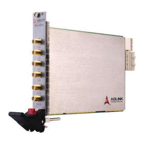
ADLINK Technology PXIe-9852 User manual

Advance Technologies; Automate the World.
PXIe-9852
2-CH 14-Bit 200 MS/s Digitizer
User’s Manual
Manual Rev.: 2.00
Revision Date: Dec. 29, 2013
Part No: 50-17047-1000

ii
Revision History
Revision Release Date Description of Change(s)
2.00 12/29/2013 Initial Release

Preface iii
PXIe-9852
Preface
Copyright 2014 ADLINK Technology, Inc.
This document contains proprietary information protected by copy-
right. All rights are reserved. No part of this manual may be repro-
duced by any mechanical, electronic, or other means in any form
without prior written permission of the manufacturer.
Disclaimer
The information in this document is subject to change without prior
notice in order to improve reliability, design, and function and does
not represent a commitment on the part of the manufacturer.
In no event will the manufacturer be liable for direct, indirect,
special, incidental, or consequential damages arising out of the
use or inability to use the product or documentation, even if
advised of the possibility of such damages.
Environmental Responsibility
ADLINK is committed to fulfill its social responsibility to global
environmental preservation through compliance with the Euro-
pean Union's Restriction of Hazardous Substances (RoHS) direc-
tive and Waste Electrical and Electronic Equipment (WEEE)
directive. Environmental protection is a top priority for ADLINK.
We have enforced measures to ensure that our products, manu-
facturing processes, components, and raw materials have as little
impact on the environment as possible. When products are at their
end of life, our customers are encouraged to dispose of them in
accordance with the product disposal and/or recovery programs
prescribed by their nation or company.
Conventions
Take note of the following conventions used throughout this
manual to make sure that users perform certain tasks and
instructions properly.

iv Preface
NOTE:
NOTE:
Additional information, aids, and tips that help users perform
tasks.
CAUTION:
Information to prevent minor physical injury, component dam-
age, data loss, and/or program corruption when trying to com-
plete a task.
Information to prevent serious physical injury, component
damage, data loss, and/or program corruption when trying to
complete a specific task.

Table of Contents v
PXIe-9852
Table of Contents
Preface .................................................................................... iii
List of Figures ....................................................................... vii
List of Tables.......................................................................... ix
1 Introduction ........................................................................ 1
1.1 Features............................................................................... 1
1.2 Applications ......................................................................... 2
1.3 Specifications....................................................................... 2
1.3.1 Analog Input ............................................................... 2
1.3.2 Timebase.................................................................... 4
1.3.3 Triggers ...................................................................... 5
1.3.4 General Specifications................................................ 6
1.4 Software Support ................................................................. 7
1.4.1 SDK ............................................................................ 7
1.4.2 WD-DASK................................................................... 7
1.5 Device Layout and I/O Array................................................ 8
2 Getting Started ................................................................. 11
2.1 Installation Environment .................................................... 11
2.2 Installing the Module.......................................................... 12
3 Operations ........................................................................ 15
3.1 Functional Block Diagram.................................................. 15
3.2 Analog Input Channel ........................................................ 15
3.2.1 Analog Input Front-End Configuration ...................... 15
3.2.2 Input Range and Data Format .................................. 16
3.2.3 DMA Data Transfer................................................... 16
3.3 Trigger Source and Trigger Modes.................................... 18
3.3.1 Software Trigger ....................................................... 19

vi Table of Contents
3.3.2 External Digital Trigger ............................................. 19
3.3.3 PXI STAR Trigger ..................................................... 19
3.3.4 PXIe_DSTARB Trigger ............................................. 20
3.3.5 PXI Trigger Bus ........................................................ 20
3.3.6 Analog Trigger .......................................................... 20
3.3.7 Trigger Export ........................................................... 21
3.4 Trigger Modes.................................................................... 21
3.4.1 Post Trigger Mode .................................................... 21
3.4.2 Delayed Trigger Mode .............................................. 21
3.4.3 Pre-Trigger Mode...................................................... 22
3.4.4 Middle Trigger Mode.................................................23
3.4.5 Acquisition with Re-Triggering .................................. 23
3.4.6 Data Average Mode (Post-Trigger and
Delayed-Trigger only) ............................................... 24
3.5 Timebase ........................................................................... 25
3.5.1 Internal Reference Clock .......................................... 25
3.5.2 External Reference Clock ......................................... 25
3.5.3 External Sampling Clock........................................... 25
3.5.4 PXI_CLK10 Clock ..................................................... 26
3.5.5 PXI_CLK100 Clock ................................................... 26
3.6 ADC Timing Control ........................................................... 26
3.6.1 Timebase Architecture.............................................. 26
3.6.2 Basic Acquisition Timing...........................................26
3.7 Synchronizing Multiple Modules ........................................ 29
A Appendix: Calibration....................................................... 31
A.1 Calibration Constant .......................................................... 31
A.2 Auto-Calibration ................................................................. 31
Important Safety Instructions.............................................. 33
Getting Service ..................................................................... 35

List of Figures vii
PXIe-9852
List of Figures
Figure 1-1: Analog Input Channel Bandwidth, ±0.2 Vpp............... 3
Figure 1-2: Analog Input Channel Bandwidth, ±2 Vpp.................. 4
Figure 1-3: PXIe-9852 Schematic................................................. 8
Figure 1-4: PXIe-9852 I/O Array ................................................... 9
Figure 3-1: Analog Input Architecture of the PXIe-9852 ............. 15
Figure 3-2: Linked List of PCI Address DMA Descriptors ........... 18
Figure 3-3: Trigger Architecture of the PXIe-9852 ...................... 18
Figure 3-4: External Digital Trigger ............................................. 19
Figure 3-5: Post-Trigger Acquisition ........................................... 21
Figure 3-6: Delayed Trigger Mode Acquisition............................ 22
Figure 3-7: Pre-Trigger Mode Acquisition ................................... 22
Figure 3-8: Middle Trigger Mode Acquisition .............................. 23
Figure 3-9: Re-Trigger Mode Acquisition .................................... 24
Figure 3-10: PXIe-9852 Clock Architecture .................................. 25
Figure 3-11: PXIe-9852 Timebase Architecture............................ 26
Figure 3-12: Basic Digitizer Acquisition Timing............................. 27
Figure 3-13: Varying Sampling Rates by Adjusting Scan Interval
Counter28

viii List of Figures
This page intentionally left blank.

List of Tables ix
PXIe-9852
List of Tables
Table 1-1: Timebase......................................................................... 5
Table 1-2: Trigger Source & Mode.................................................... 5
Table 1-3: Digital Trigger Input ......................................................... 5
Table 1-4: Digital Trigger Output....................................................... 6
Table 1-5: PXIe-9852 I/O Array Legend ......................................... 10
Table 3-1: Input Range and Data Format ....................................... 16
Table 3-2: Input Range FSR and –FSR Values.............................. 16
Table 3-3: Input Range Midscale Values........................................ 16
Table 3-4: Counter Parameters and Description ............................ 29

x List of Tables
This page intentionally left blank.

Introduction 1
PXIe-9852
1 Introduction
The PXIe-9852 is a high-speed 2-CH 14-Bit 200 MS/s digitizer,
specifically designed for applications such as LIDAR testing, opti-
cal fiber testing and radar signal acquisition. Analog input with 90
MHz bandwidth receives ±10V high speed signals with 50
impedance, and a simplified front-end design and highly stable
onboard reference provide both highly accurate measurement
results and high dynamic performance.
Ideal for environments requiring real-time acquisition and transfer
of data, the PXIe-9852 is based on the PCI Express Gen 2 x4 bus
as interface. When signals are converted from analog to digital,
continual data transfer to host system memory is enabled by PCI
Express high bandwidth capability.
The PXIe-9852 is auto-calibrated with an onboard reference circuit
calibrating offset and acquiring analog input errors. Following
auto-calibration, the calibration constant is stored in EEPROM,
such that these values can be loaded and used as needed by the
board. There is no requirement to calibrate the module manually.
1.1 Features
XPXI Express specification Rev. 1.0 compliant
XUp to 200 MS/s sampling rate
X2 simultaneous analog inputs
XHigh resolution 14-Bit ADC
XUp to 90 MHz bandwidth for analog input
XOne GB onboard storage memory
XScatter-Gather DMA data transfer for high-speed data
streaming
XSupports signal averaging
XSupport for:
Zone external digital trigger input
Zone digital trigger output to external instrument
Zone external clock input
Zauto-calibration

2 Introduction
1.2 Applications
XDistributed Temperature Sensing (DTS)
XVideo IC testing
XPhysics laboratory and research environments
XCable fault location and partial discharge monitoring for
power applications
1.3 Specifications
1.3.1 Analog Input
Channel Characteristics Comment
Channels 2 single-ended
Connector type SMA
Input coupling AC or DC, software
selectable
AC coupling cutoff
frequency 11 Hz
ADC resolution 14-Bit
Input signal range ±0.2V, ±2V or ±10V
Bandwidth (-3dB) 90 MHz
Overvoltage
±10V 1M
±10V sinewave / 7Vrms
with |Peaks| < 10V 50
Input impedance 50or 1M, software
selectable
Offset error ±1 mV
Gain error ±0.65%
SNR
56dB 1M, ±0.2V
62dB 1M, ±2V
62dB 1M, ±10V
60dB 50, ±0.2V
62dB 50, ±2V

Introduction 3
PXIe-9852
Figure 1-1: Analog Input Channel Bandwidth, ±0.2 Vpp
THD
-73dB 1M, ±0.2V
-69dB 1M, ±2V
-65dB 1M, ±10V
-73dB 50, ±0.2V
-69dB 50, ±2V
SFDR
72dB 1M, ±0.2V
72dB 1M, ±2V
72dB 1M, ±10V
68dB 50, ±0.2V
68dB 50, ±2V
CrossTalk -80dB ±0.2V, ±2V
CAUTION:
While ±10V, 50acquisition is available, overvoltage protec-
tion only applies to 7Vrms. Any ±10V sine wave with an offset
or DC voltage over ±7V input can cause damage.
Channel Characteristics Comment
0.1M 0.3M 1M 3M 10M 30M 100M 300M
−9
−8
−7
−6
−5
−4
−3
−2
−1
0
Bandwidth
Frequency (Hz)
Magnitude (dB)

4 Introduction
Figure 1-2: Analog Input Channel Bandwidth, ±2 Vpp
1.3.2 Timebase
Sample Clock Comment
Timebase options
Internal : on board synthesizer
External : CLK IN (front panel),
PXI_CLK10, and PXIe_CLK100
Sampling clock
frequency
Internal : 200MHz 3.052kS/s to
200MS/s
External : 40MHz ~ 200MHz
(CLK IN)
Timebase accuracy < ± 25ppm
External reference
clock source
Front panel, PXI_CLK10, and
PXIe_CLK100
0.1M 0.3M 1M 3M 10M 30M 100M 300M
−9
−8
−7
−6
−5
−4
−3
−2
−1
0
Bandwidth
Frequency (Hz)
Magnitude (dB)

Introduction 5
PXIe-9852
Table 1-1: Timebase
1.3.3 Triggers
Table 1-2: Trigger Source & Mode
Table 1-3: Digital Trigger Input
External reference
clock 10MHz
External reference
clock input range 500mVpp ~ 5Vpp
AC / DC
compliant, 50
load
impedance
External sampling
clock input range 1Vpp ~ 5Vpp
AC / DC
compliant, 50
load
impedance
Trigger Source & Mode
Trigger source Software, external digital trigger, analog trigger,
PXI_STAR, PXI_trigger bus [0..7], and PXIe_DSTARB
Trigger mode Post trigger, delay trigger, pre-trigger, or middle trigger,
re-trigger for post trigger and delay trigger modes
Digital Trigger Input
Sources Front panel SMA connector
Compatibility 3.3 V TTL, 5 V tolerant
Input high threshold 2.0 V
Input low threshold (VIL) 0.8 V
Maximum input overload -0.5 V ~ +5.5 V
Trigger polarity Rising or falling edge
Pulse width 20 ns minimum
Sample Clock Comment

6 Introduction
Table 1-4: Digital Trigger Output
1.3.4 General Specifications
Digital Trigger Output
Compatibility 5 V TTL
Output high threshold (VOH) 2.4 V
Output low threshold (VOL) 0.2 V
Trigger polarity Positive or negative
Pulse width 50 ns, 100 ns, 150 ns, 200 ns, 500
ns, 1 s, 2 s, 7.5 s, and 10 s
Trigger output driving capacity Capable of driving 50load
Specifications
Physical dimensions 160 (W) x 100 (H) mm (6.24 x 3.9 in.)
Bus
Bus interface PCI Express Gen 2 x 4
Environmental Tolerance
Operating Temperature: 0°C - 55°C
Relative humidity: 5% - 95%, non-condensing
Storage Temperature: -20°C - +80°C
Relative humidity: 5% - 95%, non-condensing
Calibration
Onboard reference +5 V and +2.5 V
Temperature coefficient 3.0 ppm/°C
Warm-up time 15 minutes
Power Consumption
Power Rail Standby Current (mA) Full Load (mA)
+3.3 V 766 782
12 V 882 970

Introduction 7
PXIe-9852
1.4 Software Support
ADLINK provides versatile software drivers and packages to suit
various user approaches to building a system. Aside from pro-
gramming libraries, such as DLLs, for most Windows-based sys-
tems, ADLINK also provides drivers for other application
environments such as LabVIEW®.
All software options are included in the ADLINK All-in-One CD.
Commercial software drivers are protected with licensing codes.
Without the code, you may install and run the demo version for
trial/demonstration purposes for only up to two hours. Contact
your ADLINK dealer to purchase the software license.
1.4.1 SDK
For customers who want to write their own programs, ADLINK pro-
vides the following software development kits.
ZDAQPilot for Windows, compatible with various applica-
tion environments, such as VB.NET, VC.NET, VB/VC++,
BCB, and Delphi
ZDAQPilot for LabVIEW
ZToolbox adapter for MATLAB
1.4.2 WD-DASK
WD-DASK includes device drivers and DLL for Windows XP/7/8.
DLL is binary compatible across Windows XP/7/8. This
means all applications developed with WD-DASK are compati-
ble with these Windows operating systems. The development
environment may be VB, VB.NET, VC++, BCB, and Delphi, or
any Windows programming language that allows calls to a DLL.
The WD-DASK user and function reference manuals are on the
ADLINK All-in-One CD.

8 Introduction
1.5 Device Layout and I/O Array
Figure 1-3: PXIe-9852 Schematic
NOTE:
NOTE:
All dimensions are in mm
165.04
162.54
100
209.98

Introduction 9
PXIe-9852
The PXIe-9852 I/O array is labeled to indicate connectivity, as
shown.
Figure 1-4: PXIe-9852 I/O Array

10 Introduction
Table 1-5: PXIe-9852 I/O Array Legend
Name Faceplate
Legend Type Remark
CH0 N/A Blue On indicates CH0 acquisition ongoing
Off indicates CH0 acquisition stopped
CH1 N/A Blue On indicates CH1 acquisition ongoing
Off indicates CH1 acquisition stopped
Ext. Clock
Input CLK IN
SMA
Screw
Input for external reference clock or
sample clock to digitizer
Ext. Digital
Trigger
Input
TRG IN
External digital trigger input, receiving
trigger signal from external instrument
and initiating acquisition
Trigger
Output TRG OUT
Trigger output, in which every time
acquisition begins, a pulse
synchronized with Timebase clock
asserts and is output through this
connector, at pulse width
programmable from 50ns to 10s via
software
Analog
Input CH0 Analog input channel
Analog
Input CH1 Analog input channel
Table of contents
Other ADLINK Technology Measuring Instrument manuals