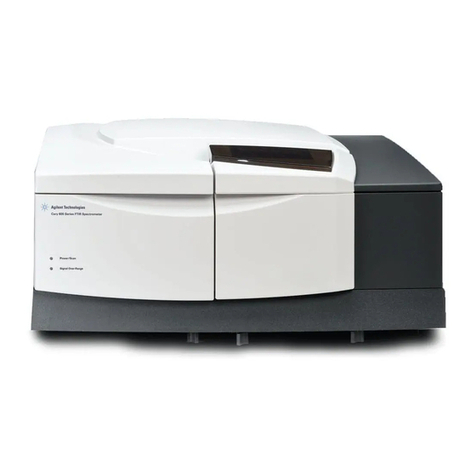
Agilent Technologies 7500 AFM User manual

Agilent 7500 AFM
Data Sheet
Features and Benefits
Atomic resolution imaging with
closed loop 90µm scanner
temperature control
Superior scanning in fluids, gases,
and ambient conditions
characterization
Unprecedented electrochemistry
Applications
Materials science
Polymer science
Nanolithography
System Overview
The Agilent 7500 AFM establishes
measurement, characterization, and
loop scanner with atomic resolution,
capabilities, and much more.
most used AFM imaging modes are
supported by the system’s standard nose
cone, which can easily be interchanged
with specialized nose cones as needed,
the Agilent 7500 is the new gold
science, materials science, polymer
science, electrical characterization, and
nanolithography.
New AFM Design
as under controlled temperature and
The scanner’s standard nose cone
The Agilent 7500 AFM System.

The 7500 scanner.
and can be utilized in a wide range
to less than 1.7µm. Open access to the
calibrate.
Environmental and
Temperature Control
demanding nanoscience applications.
accessible, sealed sample compartment
The system’s scanner resides outside the
air, in fluids, or with electrochemistry.
Agilent’s temperature control system
employs a patented thermal insulation
industry’s most precise temperature
allows imaging during temperature
imaging modes, including those utilized
in fluids. The temperature controller’s
2resolution and control to match any
MAC Mode
greatly enhanced, yielding a significant
Figure 1. Topography image (left) of polished duplex stainless steel. MFM image (right)
showing ferrite and Austenite domains of the duplex stainless steel. Scan size: 10µm.
Figure 4. Closed-loop topography image of
C36H74. Scan size: 162nm.
Figure 2. High resolution closed-loop MAC
mode image of bacteriorhodopsin, revealing
the donut-like structure of bacteriorhodopsin
trimers, and the connecting fibrous arms in
between. Scan size: 120nm.
Figure 3. Closed-loop contact mode,
topography images of atoms on mica.
Scan size: 10nm.
Electrochemistry
with electrochemistry accessories
that include a fluid cell, a salt bridge,
in
situwith precise temperature control, it is
electrochemical processes that would
otherwise be inaccessible. Furthermore,
Figure 5. KFM topography (left) and surface potential (right) images of fluoroalkane F14H20
self-assembly on Si. Scan size: 4 µm. uncompromising results.
PicoTREC
between species that are engaged in
to get the same results.
Software
The 7500 AFM system utilizes Agilent’s
PicoView, an imaging and analysis
measurement data.
Figure 7. Contact mode, topography image (left) of a cell were made to characterize cell
morphology including nucleus lower right. Scan size 50µm. Elasticity map (right) of a fixed
cell. An array of force distance curves were measured at the same position as shown in
figure left. A map of elasticity modulus was constructed by analyzing the individual force
distance curves.
Figure 6. Closed-loop topographic image
of polymer isotactic polypropylene.
Scan size: 2µm.

AFM Instrumentation from
Agilent Technologies
dedicated to the timely introduction and
AFM technologies.
www.agilent.com/find/afm
Americas
Asia Pacific
Europe & Middle East
€
Product specifications and descriptions in this document
subject to change without notice.
Figure 8. Humidity-dependent anodic oxidation of a silicon surface. Side-by-side AFM
topographic images of the resulting surface after the tip-directed oxidation under a RH of
20% (left) and a RH of 90% (right), respectively. Scan size: 6 µm.
7500 System Specifications
Scanner
Z range > 12µm
System Controller
Video Microscope
1.7µm resolution
Sample Size
Standard Modes
Optional Modes
Microscope Dimensions
Potentiostat (Option)
Downloaded from www.Manualslib.com manuals search engine
Other Agilent Technologies Microscope manuals