aion Minima User manual

MINIMA RESONANT FILTER 1
PROJECT NAME
MINIMA
BASED ON
EFFECT TYPE
PROJECT SUMMARY
DOCUMENT VERSION
Mu-tron® Micro V
A simplified version of the more famous Mu-tron III envelope filter, originally designed as a lower-cost
alternative.
Envelope filter / auto-wah 1.0.0 (2023-09-08)
BUILD DIFFICULTY
Easy
Actual size is 2.3” x 1.86” (main board) and 1.78” x 0.86” (bypass board).

MINIMA RESONANT FILTER 2
TABLE OF CONTENTS
1Project Overview 7Drill Template
2Introduction & Usage 8Enclosure Layout
3-4 Parts List 9Wiring Diagram
5Build Notes 10 Licensing
6Schematic 10 Document Revisions
INTRODUCTION
The Minima Resonant Filter is based on the Mu-tron Micro V envelope filter, designed by Mike Biegel
and first released in the mid-1970s as a lower-cost alternative to the Mu-tron III.
The Micro V has a very practical origin story. The original Mu-tron Phasor (now referred to as the
Phasor I) used CA3080 OTAs for the phase stages. When this was discontinued in favor of the more
popular Phasor II, the company had a lot of surplus CA3080 chips and no active products that used
them. At the same time, they realized they didn’t have any low-cost pedal offerings. The Micro V was
designed with the goal of filling both needs.
The end result is a similar effect to the Mu-tron III, but with a completely different circuit topology.
It was discontinued in 1980 along with the other pedals in the Mu-tron lineup not long after the
company’s sale to ARP.
The Minima is a slightly expanded version of the original Micro V circuit. The two fixed resistors that set
the attack and release of the envelope detector have been made variable, and we’ve added a third in-
between position to the “Hi/Lo” switch. It also replaces the CA3080 with the LM13700, which performs
identically but is much easier to find.
USAGE
The Minima has the following controls:
• Range sets the reaction of the filter in response to the input signal. As it’s turned up, it’s much more
sensitive and responds more quickly.
• Attack sets the time constant of the filter’s rise to the peak frequency.
• Decay sets the time constant of the filter’s fall back to the resting state.
• Frequency (toggle switch) selects the frequency range of the filter, with Low and Hi settings as well
as an in-between Mid.

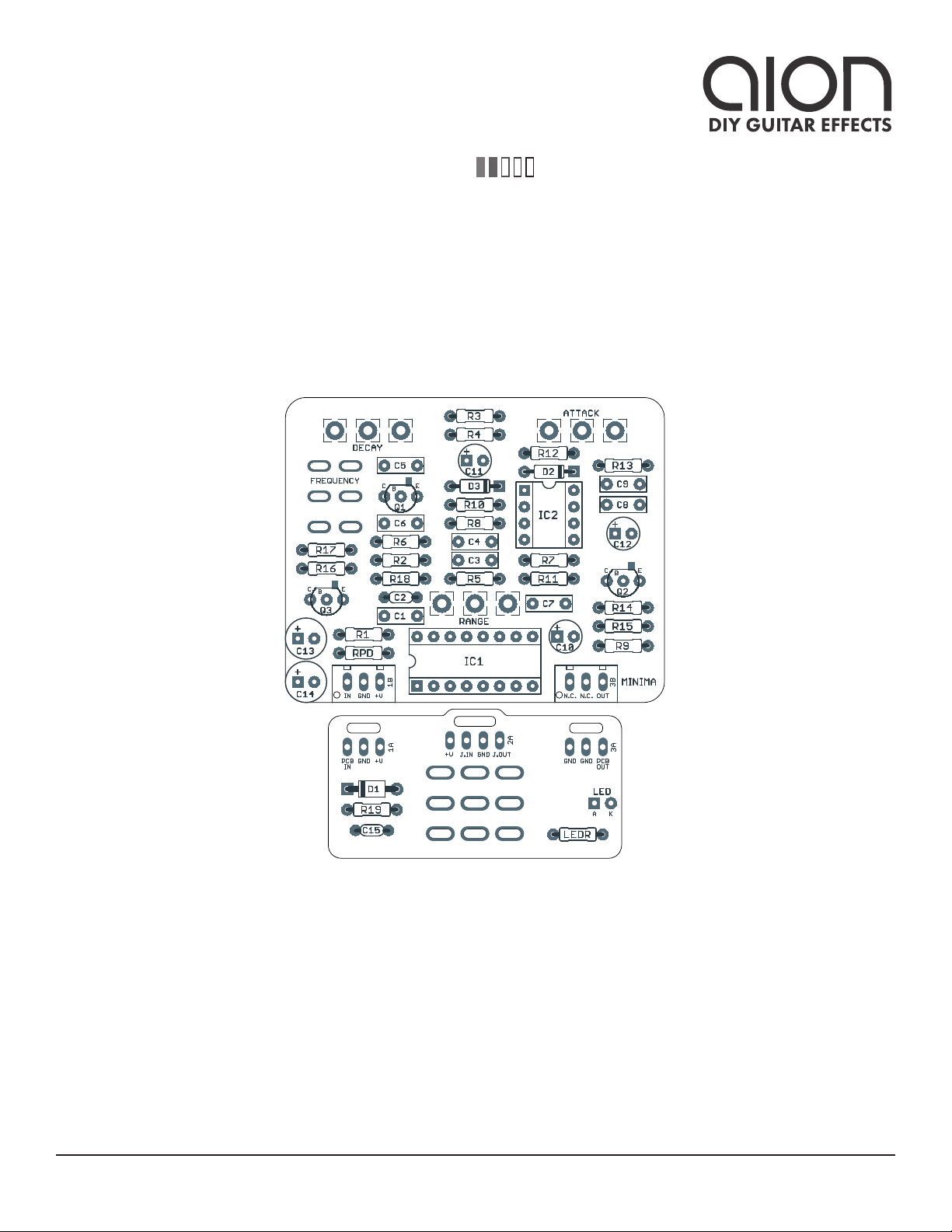
MINIMA RESONANT FILTER 3
PARTS LIST
This parts list is also available in a spreadsheet format which can be imported directly into Mouser for
easy parts ordering. Mouser doesn’t carry all the parts (most notably potentiometers) so the second tab
lists all the non-Mouser parts as well as sources for each.
View parts list spreadsheet →
PART VALUE TYPE NOTES
R1 100k Metal film resistor, 1/4W
R2 100k Metal film resistor, 1/4W
R3 10k Metal film resistor, 1/4W
R4 47R Metal film resistor, 1/4W
R5 330R Metal film resistor, 1/4W
R6 330R Metal film resistor, 1/4W
R7 6k8 Metal film resistor, 1/4W
R8 47k Metal film resistor, 1/4W
R9 22k Metal film resistor, 1/4W
R10 15k Metal film resistor, 1/4W
R11 22k Metal film resistor, 1/4W
R12 220R Metal film resistor, 1/4W Part of the Attack pot modification. Original uses 680R here.
R13 10k Metal film resistor, 1/4W Part of the Decay pot modification. Original uses 47k here.
R14 1M Metal film resistor, 1/4W
R15 4k7 Metal film resistor, 1/4W
R16 22k Metal film resistor, 1/4W
R17 33k Metal film resistor, 1/4W
R18 100k Metal film resistor, 1/4W
R19 47R Metal film resistor, 1/4W Power supply filter resistor.
RPD 2M2 Metal film resistor, 1/4W Input pulldown resistor. Can be as low as 1M.
LEDR 10k Metal film resistor, 1/4W LED current-limiting resistor. Adjust value to change LED brightness.
C1 100n Film capacitor, 7.2 x 2.5mm
C2 100pF MLCC capacitor, NP0/C0G
C3 47n Film capacitor, 7.2 x 2.5mm
C4 33n Film capacitor, 7.2 x 2.5mm
C5 68n Film capacitor, 7.2 x 2.5mm
C6 33n Film capacitor, 7.2 x 2.5mm
C7 2n2 Film capacitor, 7.2 x 2.5mm
C8 2n2 Film capacitor, 7.2 x 2.5mm
C9 1n8 Film capacitor, 7.2 x 2.5mm
C10 10uF Electrolytic capacitor, 5mm
C11 4.7uF Electrolytic capacitor, 4mm

MINIMA RESONANT FILTER 4
PARTS LIST, CONT.
PART VALUE TYPE NOTES
C12 4.7uF Electrolytic capacitor, 4mm
C13 100uF Electrolytic capacitor, 6.3mm Reference voltage filter capacitor.
C14 100uF Electrolytic capacitor, 6.3mm Power supply filter capacitor.
C15 100n MLCC capacitor, X7R Power supply filter capacitor.
D1 1N5817 Schottky diode, DO-41
D2 1N914 Fast-switching diode, DO-35
D3 1N914 Fast-switching diode, DO-35
IC1 LM13700N Transconductance amplifier, DIP16
IC1-S DIP-16 socket IC socket, DIP-16
IC2 LM1458 Operational amplifier, dual, DIP8
IC2-S DIP-8 socket IC socket, DIP-8
Q1 2N5088 BJT transistor, NPN, TO-92 Can substitute any NPN, e.g. 2N3904.
Q2 2N5087 BJT transistor, PNP, TO-92 Can substitute any PNP, e.g. 2N3906.
Q3 2N5088 BJT transistor, NPN, TO-92 Can substitute any NPN, e.g. 2N3904.
RANGE 1MB 16mm right-angle PCB mount pot
ATTACK 2kB 16mm right-angle PCB mount pot
DECAY 100kB 16mm right-angle PCB mount pot
FREQ. DPDT on-off-on Toggle switch, DPDT center off
IN 1/4" stereo 1/4" phone jack, closed frame Switchcraft 112BX or equivalent.
OUT 1/4" mono 1/4" phone jack, closed frame Switchcraft 111X or equivalent.
DC 2.1mm DC jack, 2.1mm panel mount Mouser 163-4302-E or equivalent.
BATT Battery snap 9V battery snap Optional. Use the soft plastic type—the hard-shell type will not fit.
FSW 3PDT Stomp switch, 3PDT
ENC 125B Enclosure, die-cast aluminum Can also use a Hammond 1590N1.

MINIMA RESONANT FILTER 5
BUILD NOTES
R4 resistor
A 47R resistor has been added to this circuit so that the output impedance of Q1 does not have an
adverse affect on the filter peak. It limits the high frequency bandwidth when the effect is in “Hi” mode.
This resistor mod was suggested by Rob Strand on DIYSB. Note that it’s a mostly theoretical addition—
we didn’t do any extensive testing. We recommend keeping it in place by default but you can jumper it if
you want.
Frequency switch
The frequency switch on the original Micro V is a 2-position switch with “Lo” and “Hi” modes. The
Minima adds a 3rd mode in between the other two with the use of a DPDT on-off-on switch. “Lo” is
the bottom position, “Hi” is in the middle, and “Mid” is the top position. (Note that the original Micro
V factory schematic reverses the “hi” and “lo” labels; the circuit is in “hi” mode when the resistor and
capacitor are disconnected, not when they are engaged.)
To tweak the frequency of the “Mid” mode, you can try reducing the value of C6, e.g. 22n or 15n.
Attack and Decay knobs
The original Micro V circuit only had a Range knob and a Frequency switch, in keeping with its low-cost
philosophy. However, it’s pretty straightforward to add both Attack and Decay knobs, so we’ve included
these by default. Here are the specifics on the changes:
• R12 is a 680R resistor in the original unit. This has been replaced by a 220R resistor to set the
minimum, and a 2kB potentiometer for an Attack control. The original attack value is found
between 9:00 and 10:00 on the rotation.
• R13 is a 47k resistor in the original unit. This has been replaced by a 10k resistor to set the
minimum, and a 100kB potentiometer for a Decay control. The original decay value is found
between 11:00 and 12:00 on the rotation.

SCHEMATIC
MINIMA RESONANT FILTER 6
GND
2M2
1N5817
100uF
2kB
100kB
GND
1MB
+9V
100n
VA
47R 22k
33k
GND
2N5088
100k
GND
100uF
VA
VB
GND
100n
100k
100k
VB
100pF
VB
2N5088
VA
10k
GND
4.7uF
47n 33n
LM13700N
LM13700N
LM13700N
LM13700N
VA
GND
330R
VB
VB
330R
68n
VB
VB
6k8
2n2
47k
LM1458P
LM1458P
VA
GND
VB
2n2
VB
1n8
10uF
22k
GND
15k
VB
1N914
1N914
22k
220R
4.7uF
VB
10k
VB
1M
VA
4k7
VB
2N5087
GND
33n
47R
IN
OUT
RPD
D1
C14
ATTACK
1
2
3
DECAY
1
2
3
RANGE
1
2
3
C15
R19 R16
R17
Q3
R18
C13
C1
R1
R2
C2
Q1
R3
C11
C3 C4
IC1B
14
13
12
16
15
IC1_BUF1
V+
7
8
IC1A
3
4
5
1
2IC1_BUF2
V+
10
9
116
R5R6
C5
A2
A3
A1
FREQUENCY A
B2
B3
B1
FREQUENCY B
R7
C7
R8 6
5
7
IC2B
2
3
1
IC2A
84
C8
C9
C10
R9
R10
D2
D3
R11
R12
C12
R13
R14R15
Q2
C6
R4
GND

MINIMA RESONANT FILTER 7
DRILL TEMPLATE
Cut out this drill template, fold the edges and tape it to the enclosure. Before drilling, it’s recommended
to first use a center punch for each of the holes to help guide the drill bit.
Ensure that this template is printed at 100% or “Actual Size”. You can double-check this by measuring
the scale on the printed page.
Top jack layout assumes the use of closed-frame jacks like the Switchcraft 111X. If you’d rather use
open-frame jacks, please refer to the Open-Frame Jack Drill Template for the top side.
LED hole drill size assumes the use of a 5mm LED bezel, available from several parts suppliers. Adjust
size accordingly if using something different, such as a 3mm bezel, a plastic bezel, or just a plain LED.
0 1 2
CM
0 1
INCH
x: -0.65, y: +1.71 x: 0.65, y: +1.71
ø9/32” ø9/32”
x: 0, y: +0.66
ø9/32”
x: 0, y: -1.20
ø15/32”
x: -0.775, y: -1.20
ø5/16”
CENTER (0,0)
ø3/8” ø1/2”
0.385”
0.625” 0.625”
ø3/8”
OUT DC IN
125B
ATTACK
FREQUENCYRANGE
DECAY
FOOTSWITCHLED
x: +0.85, y: +0.66
ø1/4”

MINIMA RESONANT FILTER 8
ENCLOSURE LAYOUT
Enclosure is shown without jacks. See next page for jack layout and wiring.
125B

MINIMA RESONANT FILTER 9
WIRING DIAGRAM
125B
IN +VGND N.C. N.C. OUT
PCB
IN
GND +V +V JACK GND JACK
OUTIN
GND GND PCB
OUT
Shown with optional 9V battery. If battery is omitted, both jacks can be mono rather than one being stereo.
Leave the far-right lug of the DC jack unconnected.

MINIMA RESONANT FILTER 10
LICENSE & USAGE
No direct support is offered for these projects beyond the provided documentation. It’s assumed
that you have at least some experience building pedals before starting one of these. Replacements and
refunds cannot be offered unless it can be shown that the circuit or documentation are in error.
All of these circuits have been tested in good faith in their base configurations. However, not all the
modifications or variations have necessarily been tested. These are offered only as suggestions based
on the experience and opinions of others.
Projects may be used for commercial endeavors in any quantity unless specifically noted. No
attribution is necessary, though a link back is always greatly appreciated. The only usage restrictions
are that (1) you cannot resell the PCB as part of a kit without prior arrangement, and (2) you cannot
“goop” the circuit, scratch off the screenprint, or otherwise obfuscate the circuit to disguise its source.
(In other words: you don’t have to go out of your way to advertise the fact that you use these PCBs, but
please don’t go out of your way to hide it. The guitar effects industry needs more transparency, not less!)
DOCUMENT REVISIONS
1.0.0 (2023-09-08)
Initial release.
Table of contents
Other aion Music Pedal manuals

aion
aion Obsidian User manual

aion
aion IBEX User manual

aion
aion ANDROMEDA User manual

aion
aion MAELSTROM User manual

aion
aion CONSTELLATION User manual

aion
aion Gladiator Dual Drive User manual

aion
aion ASTRA SILICON FUZZ User manual

aion
aion STRATUS User manual

aion
aion ZIRCON SILICON FUZZ User manual

aion
aion TRITON MK. III User manual