Aiwa AZG-1 User manual

CD MECHANISM
AZG-1
S/M Code No. 09-001-335-3NE
English
SERVICE MANUAL
BASIC CD MECHANISM:3ZG-2 E3
3ZG-2 YE3
TYPE
SB3RMD
SB3RNMD
SB3RMDM
SB3RNMDM
YSB3RMDM
YSB3RNMDM
BASIC CD MECHANISM
3ZG-2YE3
3ZG-2 E3
DATA

2
PROTECTION OF EYES FROM LASER BEAM DURING SERVICING
VAROITUS!
Laiteen Käyttäminen muulla kuin tässä käyttöohjeessa mainit-
ulla tavalla saattaa altistaa käyt-täjän turvallisuusluokan 1 ylit-
tävälle näkymättömälle lasersäteilylle.
VARNING!
Om apparaten används på annat sätt än vad som specificeras i
denna bruksanvising, kan användaren utsättas för osynling
laserstrålning, som överskrider gränsen för laserklass 1.
Caution: Invisible laser radiation when
open and interlocks defeated avoid expo-
sure to beam.
Advarsel:Usynling laserståling ved åbning,
når sikkerhedsafbrydere er ude af funktion.
Undgå udsættelse for stråling.
CAUTION
Use of controls or adjustments or performance of procedures
other than those specified herein may result in hazardous
radiation exposure.
ATTENTION
L'utilisation de commandes, réglages ou procédures autres que
ceux spécifiés peut entraîner une dangereuse exposition aux
radiations.
ADVARSEL!
Usynlig laserståling ved åbning, når sikkerhedsafbrydereer ude
af funktion. Undgå udsættelse for stråling.
This Compact Disc player is classified as a CLASS 1 LASER
product.
The CLASS 1 LASER PRODUCT label is located on the rear
exterior.
This set employs laser. Therefore, be sure to follow carefully the
instructions below when servicing.
WARNING!
WHEN SERVICING, DO NOT APPROACH THE LASER EXIT
WITH THE EYE TOO CLOSELY. IN CASE IT IS NECESSARY TO
CONFIRM LASER BEAM EMISSION. BE SURE TO OBSERVE
FROM A DISTANCE OF MORE THAN 30cm FROM THE
SURFACE OF THE OBJECTIVE LENS ON THE OPTICAL
PICK-UP BLOCK.
CLASS 1
KLASSE 1
LUOKAN 1
KLASS 1
LASER PRODUCT
LASER PRODUKT
LASER LAITE
LASER APPARAT
Precaution to replace Optical block
(KSS-213F)
1) After the connection, remove solder shown in
the right figure.
Body or clothes electrostatic potential could ruin
laser diode in the optical block. Be sure ground
body and workbench, and use care the clothes
do not touch the diode.

3
How to Adjust the Rotating Phase of the
Gear, Main Cam
1) Push down the hooking catch of the CHAS. MECH, and
remove the TRAY.
2) Align the arrow mark of the Gear, Main Cam with the black
round mark of the CHAS, MECHA as shown below.
3) Confirm that the Slide, Mech Cam is located in the right
position, then insert the TRAY gently.
Caution: If the rotating phase of the Gear, Main Cam is
incorrectly adjusted, the chucking operation and
tray movement will have malfunction.
Align the arrow 2mark with the black
round • mark.

4
REF. NO PART NO. KANRI DESCRIPTION
NO.
REF. NO PART NO. KANRI DESCRIPTION
NO.
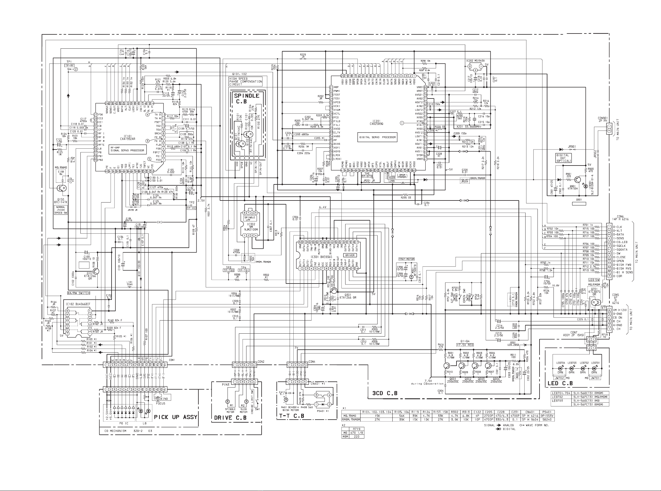
ELECTRICAL MAIN PARTS LIST
IC
87-A20-547-010 C-IC,CXA1992AR
87-017-917-080 IC,BU4066BCF
87-A20-546-010 C-IC,CXD2589Q
87-A20-592-040 C-IC,M51943 AML
87-A20-445-010 IC,BA5936
87-001-792-080 IC,NJM2100M
TRANSISTOR
89-406-555-080 TR,2SD655 (0.5W)
87-A30-071-080 C-TR,RT1N 144C
87-026-609-080 TR,KTA1266GR
87-026-239-080 TR,DTC114TK (0.2W)
87-A30-060-080 C-TR,KTC3875GR<SB3MD,SB3RMDM>
87-A30-061-080 C-TR,KTA1504GR
DIODE
87-A40-758-080 ZENER, UZ8.2BSB
87-020-465-080 DIODE,1SS133 (110MA)
3CD C.B
C1 87-010-196-080 CHIP CAPACITOR,0.1-25
C2 87-010-382-080 CAP, ELECT 22-25V
C3 87-010-384-080 CAP,E 100-25 SME
C4 87-010-196-080 CHIP CAPACITOR,0.1-25
C101 87-010-263-080 CAP, ELECT 100-10V
C102 87-010-178-080 CHIP CAP 1000P
C103 87-010-263-080 CAP, ELECT 100-10V
C104 87-010-188-080 CAP,CHIP 6800P
C105 87-010-198-080 CAP, CHIP 0.022
C106 87-016-081-080 C-CAP,S 0.1-16 RK
C107 87-016-081-080 C-CAP,S 0.1-16 RK
C108 87-016-081-080 C-CAP,S 0.1-16 RK
C109 87-010-404-080 CAP, ELECT 4.7-50V
C110 87-016-081-080 C-CAP,S 0.1-16 RK
C111 87-010-197-080 CAP, CHIP 0.01 DM
C112 87-010-402-080 CAP, ELECT 2.2-50V
C113 87-010-382-080 CAP, ELECT 22-25V
C114 87-010-213-080 C-CAP,S 0.015-50 B
C115 87-010-263-080 CAP, ELECT 100-10V
C116 87-010-197-080 CAP, CHIP 0.01 DM
C117 87-010-186-080 CAP,CHIP 4700P
C118 87-010-197-080 CAP, CHIP 0.01 DM
C119 87-016-369-080 C-CAP,S 0.033-25 B K
C120 87-010-197-080 CAP, CHIP 0.01 DM
C121 87-010-401-080 CAP, ELECT 1-50V
C122 87-010-148-080 C-CAP,S 4P-50 CH<SB3MD,SB3RNMD>
C122 87-010-154-080 CAP CHIP 10P<SB3RMDM,SB3RNMDM>
C125 87-010-596-080 CAP, S 0.047-16
C126 87-010-596-080 CAP, S 0.047-16
C127 87-012-140-080 CAP 470P
C128 87-010-596-080 CAP, S 0.047-16
C129 87-010-198-080 CAP, CHIP 0.022
C130 87-016-081-080 C-CAP,S 0.1-16 RK
C131 87-010-263-080 CAP, ELECT 100-10V
C132 87-010-263-080 CAP, ELECT 100-10V
C133 87-012-158-080 C-CAP,S 390P-50 CH
C134 87-010-196-080 CHIP CAPACITOR,0.1-25
C135 87-010-196-080 CHIP CAPACITOR,0.1-25
C136 87-010-196-080 CHIP CAPACITOR,0.1-25
C137 87-010-196-080 CHIP CAPACITOR,0.1-25
C138 87-010-152-080 C-CAP,S 8P-50 CH<SB3MD,SB3RNMD>
C139 87-010-263-080 CAP,E 100-10 M 11L SME
C150 87-010-197-080 CAP, CHIP 0.01 DM
C152 87-010-196-080 CHIP CAPACITOR,0.1-25
C202 87-010-596-080 CAP, S 0.047-16
C203 87-010-188-080 CAP,CHIP 6800P
C204 87-012-156-080 C-CAP,S 220P-50 CH
C205 87-010-183-080 C-CAP,S 2700P-50 B<SB3MD,SB3RNMD>
C205 87-010-186-080 CAP,CHIP 4700P<SB3RMDM,SB3RNMDM>
C206 87-016-526-080 C-CAP,S 0.47-16 BK
C207 87-010-197-080 CAP, CHIP 0.01 DM
C209 87-012-154-080 C-CAP,S 150P-50 CH
C210 87-012-154-080 C-CAP,S 150P-50 CH
C211 87-010-176-080 C-CAP,S 680P-50 SL
C212 87-010-176-080 C-CAP,S 680P-50 SL
C213 87-010-402-080 CAP, ELECT 2.2-50V
C214 87-010-402-080 CAP, ELECT 2.2-50V
C215 87-010-154-080 CAP CHIP 10P
C216 87-010-154-080 CAP CHIP 10P
C217 87-010-263-080 CAP, ELECT 100-10V
C218 87-010-197-080 CAP, CHIP 0.01 DM
C219 87-010-196-080 CHIP CAPACITOR,0.1-25
C220 87-010-197-080 CAP, CHIP 0.01 DM
C221 87-010-197-080 CAP, CHIP 0.01 DM
C222 87-010-197-080 CAP, CHIP 0.01 DM
C223 87-016-081-080 C-CAP,S 0.1-16 RK
C224 87-010-196-080 CHIP CAPACITOR,0.1-25
C225 87-010-196-080 CHIP CAPACITOR,0.1-25
C226 87-010-196-080 CHIP CAPACITOR,0.1-25
C227 87-010-196-080 CHIP CAPACITOR,0.1-25
C228 87-010-370-080 CAP,E 330-6.3 SME
<SB3RMDM,SB3RNMDM>
C228 87-010-371-080 CAP,E 470-6.3V<SB3MD,SB3RNMD>
C229 87-010-172-080 CAP, CHIP 330P
C230 87-010-172-080 CAP, CHIP 330P
C231 87-010-186-080 C-CAP,S 4700P-50<SB3MD,SB3RNMD>
C231 87-010-196-080 CHIP CAPACITOR,0.1-25
<SB3RMDM,SB3RNMDM>
C232 87-010-196-080 CHIP CAPACITOR,0.1-25
C233 87-010-196-080 CHIP CAPACITOR,0.1-25
C234 87-010-196-080 CHIP CAPACITOR,0.1-25
C235 87-010-263-080 CAP, ELECT 100-10V
<SB3RMDM,SB3RNMDM>
C236 87-010-196-080 CHIP CAPACITOR,0.1-25
C237 87-010-196-080 CHIP CAPACITOR,0.1-25
C302 87-010-196-080 CHIP CAPACITOR,0.1-25
C303 87-010-197-080 CAP, CHIP 0.01 DM
C304 87-A10-730-080 CAP,E 1000-16 SMG
C306 87-010-197-080 CAP, CHIP 0.01 DM
C307 87-010-196-080 CHIP CAPACITOR,0.1-25
C308 87-010-186-080 CAP,CHIP 4700P
C309 87-010-196-080 CHIP CAPACITOR,0.1-25
C310 87-010-196-080 CHIP CAPACITOR,0.1-25
C311 87-010-196-080 CHIP CAPACITOR,0.1-25
C312 87-010-196-080 CHIP CAPACITOR,0.1-25
C313 87-010-196-080 CHIP CAPACITOR,0.1-25
C398 87-010-405-080 CAP, ELECT 10-50V
C399 87-010-405-080 CAP, ELECT 10-50V
C701 87-010-322-080 C-CAP,S 100P-50 CH
C702 87-010-318-080 C-CAP,S 47P-50 CH
C703 87-010-318-080 C-CAP,S 47P-50 CH
C704 87-010-322-080 C-CAP,S 100P-50 CH
C705 87-010-178-080 CHIP CAP 1000P
C706 87-010-405-080 CAP, ELECT 10-50V
C710 87-010-196-080 CHIP CAPACITOR,0.1-25
<SB3RMDM,SB3RNMDM>
C901 87-010-260-080 CAP, ELECT 47-25V
C902 87-010-196-080 CHIP CAPACITOR,0.1-25
CON1 87-A60-429-010 CONN,16P H TOC-A
CON2 87-099-199-010 CONN,6P 6216 H
CON4 87-099-212-010 CONN,5P 6216 V
CON5 87-A60-154-010 CONN,6P H FE
CON6 87-099-031-010 CONN,14P 6216 H
CON7 84-ZG1-647-010 CONN ASSY,2P<SB3MD,SB3RMDM>

5
REF. NO PART NO. KANRI DESCRIPTION
NO.
CON901 87-009-345-010 CONN,2P PH H
L101 87-003-102-080 COIL, 10UH
L299 87-A50-189-080 C-COIL,S BLM21B272S
LED901 87-A40-558-010 LED,SLZ-8128A-01-A
M301 87-045-305-010 MOTOR, RF-500TB DC-5V (2MA)
SW701 87-036-109-010 PUSH SWITCH
SW702 87-036-109-010 PUSH SWITCH
X201 87-A70-005-080 VIB,XTAL 33.8688MHZ HC-49/U03
LED C.B<SB3MD,SB3RMDM>
LED701 87-A40-268-080 LED,SLH-56DCT31 ORN<SB3RMDM>
LED702 87-A40-263-080 LED,SLH-56PCT31 GRN
<SB3MD,SB3RMDM>
LED703 87-A40-268-080 LED,SLH-56DCT31 ORN<SB3MD>
LED703 87-A40-263-080 LED,SLH-56PCT31 GRN<SB3RMDM>
LED704 87-A40-268-080 LED,SLH-56DCT31 ORN<SB3RMDM>
T-T C.B
C401 87-A11-148-080 CAP,TC U 0.1-50 Z F
CN401 87-A60-082-010 CONN,05P H 9604S-05F
<SB3RMDM,SB3RNMDM>
CN401 86-NFZ-675-010 CONN,5P H 6216-11H<SB3MD,SB3RNMD>
M401 87-045-364-010 MOTOR(BCH3B14)
PS401 87-026-573-010 IC,GP1S53V<SB3MD,SB3RNMD>
PS401 87-A90-156-010 SNSR,SG-240<SB3RMDM,SB3RNMDM>
SPINDLE C.B
C101 87-012-142-080 C-CAP,S 0.33-16 Z F GRM
DRIVE C.B
M2 87-045-356-010 MOT,RF-310TA 30
PIN3 87-A60-086-010 CONN,6P H6216-11
SW1 87-A90-042-010 SW,LEAF MSW-17310MVP0
• Regarding connectors, they are not stocked as they are not the initial order items.
The connectors are available after they are supplied from connector manufacturers upon the order is received.
88
A
Resistor Code
Chip Resistor Part Coding
Figure
Value of resistor
Chip resistor
Wattage Type Tolerance
1/16W
1/10W
1/8W
1608
2125
3216
5%
5%
5%
CJ
CJ
CJ
Form
LW t
1.6 0.8 0.45
2 1.25 0.45
3.2 1.6
108
118
128
: A
: A
CHIP RESISTOR PART CODE
0.55
Resistor Code
Dimensions (mm)
Symbol
1/16W 1005 5% CJ
1.0 0.5 0.35 104
Lt
W

6
TRANSISTOR ILLUSTRATION
E
B
C
ECB
DTC114TK
RT1N144C
KTA1504GR
KTC3875GR
KTA1266
2SD655

87
BLOCK DIAGRAM

12345678910 11 12 13 14
A
B
C
D
E
F
G
H
I
J
K
109
WIRING-1 (3CD/LED)

1211
SCHEMATIC DIAGRAM
LED DRIVER
KSS-213F
LED
DRIVER

1413
1IC201 Pin , (XTAI, XTAO) VOLT/DIV: 1V
SYSTEM CLOCK TIME/DIV: 0.1µS
f=33.8688MHz
2TP1 (TP-RF) VOLT/DIV: 500mV
RF TIME/DIV: 0.5µS
3IC101 Pin 6(FE O) VOLT/DIV: 200mV
FOCUS TIME/DIV: 2mS
WAVE FORM
3.4V
0
4IC101 Pin #(TA O) TIME/DIV: 1mS
TRACKING
5IC101 Pin 1(FE O)
FOCUS SEARCH
VC
VC
CD: 1.0±0.2V
CD-RW: 1.0±0.2V
VC
70 71
1234567
A
B
C
D
E
F
G
H
I
J
K
WIRING-2 (T-T/MOTOR)

15
IC BLOCK DIAGRAM
IC, NJM2100M
IC, BA5936S

16
Output terminal for focus error amplifier. Internally connected to window comparator
input for bias condition.
Input terminal for focus error.
Capacitor connection terminal for time constant used when there is defect.
This pin is connected to GND via capacitor when high frequency gain of the focus
servo is attenuated.
This is a pin where the time constant is externally connected to raise the low frequency
gain of the focus servo.
Focus drive output.
Focus amplifier inverted input pin.
This is a pin where the time constant is externally connected to generate the focus
search waveform.
This is a pin where the selection time constant is externally connected to set the
tracking servo the high frequency gain.
This is a pin where the selection time constant is externally connected to set the
tracking high frequency gain.
Pin for setting peak of the phase compensator of the focus tracking.
Tracking amplifier inverted input pin.
Tracking drive output.
Sled amplifier non-inverted input pin.
Sled amplifier inverted input pin.
Sled drive output.
The current which determines height of the focus search, track jump and sled kick is
input with external resistance connected.
Power supply.
“L” setting starts sled disorder-prevention circuit. (Not pull-up resistance)
Clock input for serial data transfer from CPU. (No pull-up resistance)
Latch input from CPU. (No pull-up resistance)
Serial data input from CPU. (No pull-up resistance)
Reset system at “L” setting. (No pull-up resistance)
Signal output for track number counting.
FZC, DFCT1, TZC, BALH, TGH, FOH, or ATSC is output depending on the
command from CPU.
DFCT2, MIRR, BALL, TGL or FOL is output depending on the command from CPU.
Output terminal for focus OK comparator.
Input pin where the DEFECT bottom hold output is capacitance coupled.
DEFECT bottom-hold output terminal. Internally connected to interruption comparator
input.
Connection terminal for DEFECT bottom-hold capacitor.
Connection terminal for MIRR hold-capacitor.
Anti-reverse input terminal for MIRR comparator.
FEO
FEI
FDFCT
FGD
FLB
FE_O
FEM
SRCH
TGU
TG2
FSET
TA_M
TA_O
SL_P
SL_M
SL_O
ISET
Vcc
LOCK
CLK
XLT
DATA
XRST
C_OUT
SENS1
SENS2
FOK
CC2
CC1
CB
CP
IC, CXA1992AR
Pin No. Pin Name I/O Description
1
2
3
4
5
6
7
8
9
10
11
12
13
14
15
16
17
18
19
20
21
22
23
24
25
26
27
28
29
30
31
O
I
I
I
I
O
I
I
I
I
I
I
O
I
I
O
I
I
I
I
I
I
I
O
O
O
O
I
O
I
I
IC DESCRIPTION

17
RF_I
RF_O
RF_M
RFTC
LD
PD
PD1, PD2
FEBIAS
F, E
EI
VEE
TEO
LPFI
TEI
ATSC
TZC
TDFCT
VC
FZC
Pin No. Pin Name I/O Description
32
33
34
35
36
37
38, 39
40
41, 42
43
44
45
46
47
48
49
50
51
52
I
O
I
I
O
I
I
I/O
I
—
—
O
I
I
I
I
I
O
I
Input terminal by capacity combination of RF summing amplifier.
Output terminal of RF summing amplifier. Checkpoint of Eye pattern.
Anti-reverse input terminal for RF summing amplifier.
The gain of RF amplifier is decided by the connection resistance between RF_M and
RFO terminals.
This is a pin where the selection time constant is externally connected to control the
RF level.
APC amplifier output terminal.
APC amplifier input terminal.
RFI-V amplifier inverted input pin.
These pins are connected to the A+C and B+C pins of the optical pickup, receiving by
currents input.
Bias adjustment pin of the focus error amplifier. (Not connected)
F and EIV amplifier inverted input pins.
These pins are connected to the F and E of the optical pickup, receiving by current
input.
Gain adjustment pin of the I-V amplifier E. (When not in use of BAL automatic
adjustment)
GND connection pin.
Output terminal for tacking-error amplifier. Output E-F signal.
BAL adjustment comparator input pin. (Input through LPF from TEO)
Input terminal for tracking error.
Window-comparator input terminal for detecting ATSC.
Input terminal for tracking-zero cross comparator.
Capacitor connection pin for the time constant used when there is defect.
Output terminal for DC voltage reduced to half of VCC+VEE.
Input terminal for focus-zero cross comparator.

18
GND.
Lch-“0” detect flag. (Not connected)
Rch-“0” detect flag. (Not connected)
Clock input for SQSO read out.
SubQ 80 bit serial output.
SENS signal output to CPU.
Serial data input from CPU.
Latch input from CPU, Latch serial data at fall down.
Clock input to serial data transfer from CPU.
SENS input from SSP.
Numbers of track jump are counted and input.
Serial data output to SSP.
Serial-data latch output to SSP. Latch at fall down.
Clock output for serial data transfer to SSP.
Microcomputer expansion interface. (Input A)
Microcomputer expansion interface. (Input B)
Microcomputer expansion interface. (Output)
Focus OK input terminal. Used for SENS output and servo-auto sequencer.
Power supply. (+5V)
Servo control for spindle motor.
External control input for spindle motor. (Not connected)
TEST terminal. (Connected to GND)
Charge pump output for extensive EFM PLL.
VCO2 oscillator input for extensive EFM PLL.
VCO2 oscillator output for extensive EFM PLL.
VCO2 control voltage input for extensive EFM PLL.
Charge pump output for master PLL.
Filter (slave = digital PLL) output for master PLL.
Filter input for master PLL.
Analog GND.
VCO control voltage input for master.
Analog power. (+5V)
EFM signal input.
Constant current input to asymmetry circuit.
Comparison voltage input to asymmetry circuit.
EFM full-swing output. (L=VSS, H=VDD)
D/A interface, LR clock output f=FS.
LR clock input.
D/A interface, serial data output. (2’s COMP, MSB first)
D/A interface, serial data input. (2’s COMP, MSB first)
VSS
LMUT
RMUT
SQCK
SQSO
SENS
DATA
XLAT
CLOK
SEIN
CNIN
DATO
XLTO
CLKO
SPOA
SPOB
XLON
FOK
VDD
MDP
PWMI
TEST
TESI
VPCO
VCKI
V16M
VCTL
PCO
FILO
FILI
AVSS
CLTV
AVDD
RF
BIAS
ASYI
ASYO
LRCK
LRCKI
PCMD
PCMDI
IC, CXD2589Q
Pin No. Pin Name I/O Description
1, 20, 45, 60
2
3
4
5
6
7
8
9
10
11
12
13
14
15
16
17
18
19, 46, 61, 80
21
22
23
24
25
26
27
28
29
30
31
32
33
34
35
36
37
38
39
40
41
42
—
O
O
I
O
O
I
I
I
I
I
O
O
O
I
I
O
I
—
O
I
I
I
O
I
O
I
O
O
I
—
I
—
I
I
I
O
O
I
O
I

19
D/A interface bit clock output.
D/A interface bit clock input.
XUGF output, MNT1 or RPCK output by switching command. (Not connected)
XPLCK output, MNT0 output by switching command. (Not connected)
GFS output, MNT3 or XRAOF output by switching command.
C2PO output, GTOP output by switching command. (Not connected)
X’tal select input terminal, X’tal: 16.9344MHz = “L” 33.8688MHz = “H”.
4.2336MHz output, Output 1/4 divided frequency of VCKI at CAV-W mode.
(Not connected)
Digital Out connector output signal.
“H” when the playback disc has emphasis. “L” when it does not.
De-emphasis ON/OFF, “H” when ON, “L” when OFF.
WFCK output. (Not connected)
H output when the subcode sync S0 or S1 is detected. (Not connected)
Serial output for SubP-W. (Not connected)
SBSO read out clock input.
Mute input terminal, Active the “H” setting.
Analogue GND.
Analogue power supply. (+5V)
Lch/analogue output terminal.
Lch/OP AMP input terminal.
Lch/LINE output terminal.
Analogue GND.
Power supply for master clock.
Input terminal for crystal oscillator circuit.
Input external master clock from this terminal.
Output terminal for crystal oscillator circuit.
GND terminal for master clock.
Analogue GND.
Rch/LINE output terminal.
Rch/OP AMP input terminal.
Rch/analogue output terminal.
Analogue power supply. (+5V)
Analogue GND.
Reset system at “L” setting.
BCK
BCKI
XUGF
XPCK
GFS
C2PO
XTSL
C4M
DOUT
EMPH
EMPHI
WFCK
SCOR
SESO
EXCK
SYSM
AVSS
AVDD
AOUT1
AIN1
LOUT1
AVSS
XVDD
XTAI
XTAO
XVSS
AVSS
LOUT2
AIN2
AOUT2
AVDD
AVSS
XRST
Pin No. Pin Name I/O Description
43
44
47
48
49
50
51
52
53
54
55
56
57
58
59
62
63
64
65
66
67
68
69
70
71
72
73
74
75
76
77
78
79
O
I
O
O
O
O
I
O
O
O
I
O
O
O
I
I
—
—
O
I
O
—
—
I
O
—
—
O
I
O
—
—
I
Note) • PCMD is the two’s complement output with MSB first.
• GTOP monitors the protection status of the Frame Sync. (H: Sync protection window opened).
• XUGF is the Frame Sync negative pulse which is obtained from the EFM signal. This is the signal before the sync protection.
• XPLCK is the inverted signal of the EFM PLL clock. The PLL works so that the fall-down edge and the changed point of the
EFM signal agree.
• GFS is the signal that goes “H” when the Frame Sync and the internally inserted timing agree.
• RFCK is the signal having 136 micro-seconds (during normal speed) that is generated to have the same accuracy as X’tal.
• C2PO is the signal indicating the error status of the data.
• XRAOF is the signal that is generated when the 16k RAM goes outside the jitter margin ±4F.

20
MECHANICAL EXPLODED VIEW 1/1
3ZG-2
A
B
1
4
3
P.C.B
AZA-9
32
34
35
CUSHION,CD A
CUSHION,
CD A
CUSHION,CD A
P.C.B
5
7
8
9
aa
10
11
12
13
14
15
15
33
17
18
4
21
22
23
24
25
26
27
28 29 30
19
31
20
2
6
SH, 2.5-40-0.5 PC
16
LED 901

21
REF. NO PART NO. KANRI DESCRIPTION
NO.
REF. NO PART NO. KANRI DESCRIPTION
NO.
MECHANICAL PARTS LIST 1/1
1 84-ZG1-225-010 BELT,SQ1.0-63.3
2 84-ZG1-672-010 F-CABLE,5P 1.25 210MM WHITE N
3 87-045-364-010 MOTOR(BCH3B14)
4 84-ZG1-267-010 PULLEY,LOAD MO 8
<EXCEPT SB3RMD,SB3RNMD>
4 81-ZG1-212-010 PULLY,LOAD MO<SB3RMD,SB3RNMD>
5 84-ZG1-238-010 GEAR,WORM N
6 84-ZG1-248-010 SPR-C,WORM
7 84-ZG1-239-210 PULLY,WORM N
8 8A-ZG1-001-010 TRAY,NO3 BLU
9 84-ZG1-291-110 HLDR,MAGNET 4 NAT
<YSB3RNMDM,SB3RNMDM,SB3RNMD>
9 84-ZG1-272-110 HLDR,MAGNET N 4
<SB3RMD,SB3RMDM,YSB3RNMDM>
10 84-ZG1-259-010 SPR-P,WORM
11 84-ZG1-269-010 GEAR,MAIN TT 4
12 84-ZG1-224-010 LEVER,TT
<SB3RMD,SB3RMDM,YSB3RNMDM>
12 84-ZG1-288-010 LEVER,TT NAT
<YSB3RNMDM,SB3RNMDM,SB3RNMD>
13 8A-ZG1-002-010 TURN TABLE,NO1 BLU
14 81-ZG1-239-010 S-SCREW,TT
15 81-ZG1-271-010 S-SCREW MECH REAR
16 85-NFT-611-110 FF-CABLE 16P-1.0
17 84-ZG1-287-010 HLDR,MECHA NAT
<YSB3RNMDM,SB3RNMDM,SB3RNMD>
17 84-ZG1-212-210 HLDR,MECHA NO2
<SB3RMD,SB3RMDM,YSB3RNMDM>
18 87-045-305-010 MOTOR, RF-500TB DC-5V (2MA)
19 84-ZG1-211-010 SPR-E CAM S
20 81-ZG1-255-110 PLATE,MAGNET MK2
21 83-ZG3-604-010 RING,MAG 2
22 83-ZG3-213-010 LVR,SW
23 84-ZG1-266-010 LEVER,CAN 8
24 84-ZG1-205-210 GEAR,TRAY (*)
25 81-ZG1-291-110 GEAR,TRAY RELAY NO3
26 84-ZG1-274-010 GEAR,RELAY 8
27 84-ZG1-207-010 PULLEY,RELAY
28 84-ZG1-209-010 BELT,SQ1.8-117.7
29 84-ZG1-203-410 GEAR,MAIN CAM
<YSB3RNMDM,SB3RNMDM,SB3RNMD>
29 84-ZG1-215-410 GEAR,MAIN CAM BLU
<SB3RMD,SB3RMDM,YSB3RNMDM>
30 84-ZG1-011-010 REFLECTOR,CD
<SB3RMD,SB3RMDM,YSB3RNMDM>
31 84-ZG1-216-310 SLIDE,MECHA CAM YEL
<SB3RMD,SB3RMDM,YSB3RNMDM>
31 84-ZG1-204-310 SLIDER,MECHA CAM
<YSB3RNMDM,SB3RNMDM,SB3RNMD>
32 84-ZG1-201-410 CHAS,MECHA
<SB3RMD,SB3RMDM,YSB3RNMDM>
32 84-ZG1-286-010 CHAS,MECHA NAT
<YSB3RNMDM,SB3RNMDM,SB3RNMD>
33 84-ZG1-630-010 CABLE FFC 6P-1.25
34 84-ZG1-244-310 CABI,OPTICAL
35 84-ZG1-261-010 LID,OPTICAL
A 87-067-703-010 TAPPING SCREW, BVT2+3-10
<SB3RMD,SB3RMDM,YSB3RNMDM>
B 87-067-981-010 BVT2+3-6 BLK
COLOR NAME TABLE
Basic color symbol Color Basic color symbol Color Basic color symbol Color
B Black C Cream D Orange
G Green H Gray L Blue
LT Transparent Blue N Gold P Pink
R Red S Silver ST Titan Silver
T Brown V Violet W White
WT Transparent White Y Yellow YT Transparent Yellow
LM Metallic Blue LL Light Blue GT Transparent Green
LD Dark Blue DT Transparent Orange GM Metallic Green
YM Metallic Yellow DM Metallic Orange PT Transparent Pink

22
A
3
6
2
5
1
P.C.B
M2
SW1
4
CD MECHANISM EXPLODED VIEW 1/1
CD MECHANISM PARTS LIST 1/1
REF. NO PART NO. KANRI DESCRIPTION
NO.
1 83-ZG2-262-010 CHAS ASSY,E3
2 87-A90-836-010 PICKUP,KSS-213F
3 83-ZG2-235-010 GEAR,A3
4 83-ZG2-236-010 GEAR,MOTOR 3
5 83-ZG2-205-310 GEAR,B
6 83-ZG2-253-010 SHAFT,SLIDE 5
A 87-261-032-210 V+2-3

23
ELECTRICAL SECTION
DESCRIPTION REFERENCE NAME
ANT ANTENNAS
C- CHIP
C-CAP CAP, CHIP
C-CAP TN CAP, CHIP TANTALUM
C-COIL COIL, CHIP
C-DI DIODE, CHIP
C-DIODE DIODE, CHIP
C-FET FET, CHIP
C-FOTR FILTER, CHIP
C-JACK JACK, CHIP
C-LED LED, CHIP
C-RES RES, CHIP
C-SFR SFR, CHIP
C-SLIDE SW SLIDE SWITCH, CHIP
C-SW SWITCH, CHIP
C-TR TRANSISTOR, CHIP
C-VR VOLUME, CHIP
C-ZENER ZENER, CHIP
CAP, CER CAP, CERA-SOL
CAP, E CAP, ELECT
CAP, M/F CAP, FILM
CAP, TC CAP, CERA-SOL
CAP, TC-U CAP, CERA-SOL SS
CAP, TN CAP, TANTALUM
CERA FIL FILTER, CERAMIC
CF FILTER, CERAMIC
DL DELAY LINE
E/CAP CAP, ELECT
FILT FILTER
FLTR FILTER
FUSE RES RES, FUSE
MOT MOTOR
P-DIODE PHOTO DIODE
P-SNSR PHOTO SENSER
P-TR PHOTO TRANSISTOR
POLY VARI VARIABLE CAPACITOR
PPCAP CAP, PP
PT POWER TRANSFORMER
PTR, RES PTR, MELF
RC REMOTE CONTROLLER
RES NF RES, NON-FLAMMABLE
RESO RESONATOR
SHLD SHIELD
SOL SOLENOID
SPKR SPEAKER
SW, LVR SWITCH, LEVER
SW, RTRY SWITCH, ROTARY
SW, SL SWITCH, SLIDE
TC CAP CAP, CERA-SOL
THMS THERMISTOR
TR TRANSISTOR
TRIMMER CAP, TRIMMER
TUN-CAP VARIABLE CAPACITOR
VIB, CER RESONATOR, CERAMIC
VIB, XTAL RESONATOR, CRYSTAL
VR VOLUME
ZENER DIODE, ZENER
REFERENCE NAME LIST MECHANICAL SECTION
DESCRIPTION REFERENCE NAME
ADHESHIVE SHEET ADHESHIVE
AZ AZIMUTH
BAR-ANT BAR-ANTENNA
BAT BATTERY
BATT BATTERY
BRG BEARING
BTN BUTTON
CAB CABINET
CASS CASSETTE
CHAS CHASSIS
CLR COLLAR
CONT CONTROL
CRSR CURSOR
CU CUSHION
CUSH CUSHION
DIR DIRECTION
DUBB DUBBING
FL FRONT LOADING
FLY-WHL FLYWHEEL
FR FRONT
FUN FUNCTION
G-CU G-CUSHION
HDL HANDOL
HIMERON CLOTH
HINGE, BAT HINGE, BATTERY
HLDR HOLDER
HT-SINK HEAT SINK
IB INSTRUCTION BOOKLET
IDLE IDLER
IND, L-R INDICATOR, L-R
KEY, CONT KEY, CONTROL
KEY, PRGM KEY, PROGRAM
KNOB, SL KNOB, SLIDE
LBL LABEL
LID, BATT LID, BATTERY
LID, CASS LID, CASSETTE
LVR LEVER
P-SP P-SPRING
PANEL, CONT PANEL, CONTROL
PANEL, FR PANEL, FRONT
PRGM PROGRAM
PULLY, LOAD MO PULLY, LOAD MOTOR
RBN RIBBON
S- SPECIAL
SEG SEGMENT
SH SHEET
SHLD-SH SHIELD-SHEET
SL SLIDE
SP SPRING
SP-SCREW SPECIAL-SCREW
SPACER, BAT SPACER, BATTERY
SPR SPRING
SPR-P P-SPRING
SPR-PC-PUSH P-SPRING, C-PUSH
T-SP T-SPRING
TERM TERMINAL
TRIG TRIGGER
TUN TUNING
VOL VOLUME
W WASHER
WHL WHEEL
WORM-WHL WORM-WHEEL

0251431 Printed in Singapore
2–11, IKENOHATA 1–CHOME, TAITO-KU, TOKYO 110-8710, JAPAN TEL:03 (3827) 3111
Other manuals for AZG-1
3
Table of contents
Other Aiwa CD Player manuals