AKM AsahiKASEI AK4675 User manual

[AK4675]
MS0963-E-00 2008/05
- 1 -
GENERAL DESCRIPTION
The AK4675 is a stereo CODEC with a built-in Microphone-Amplifier, Receiver-Amplifier, cap-less
Headphone-Amplifier and stereo audio class-D Speaker-Amplifier. The AK4675 features dual PCM I/F in
addition to audio I/F that allows easy interfacing in mobile phone designs with Bluetooth I/F. The
Speaker-Amplifier includes ALC (Automatic Level Control) circuit what is able to stabilize each output
sound levels. The AK4675 is available in an 83pin BGA, utilizing less board space than competitive
offerings.
FEATURES
1. Recording Function (Stereo CODEC)
•4 Stereo Input Selector x 2ch
•4 Stereo Inputs (Single-ended) or 2 Stereo Input (Full-differential)
•MIC Amplifier: +30dB ∼−12dB, 3dB step
•Digital ALC (Automatic Level Control): +36dB ∼−54dB, 0.375dB Step, Mute
•Wind-noise Reduction Filter
•Stereo Separation Emphasis
•5-band Programmable Notch Filter
•Audio Interface Format: 16bit MSB justified, I2S, DSP Mode
2. Playback Function (Stereo CODEC)
•Digital Volume (+12dB ∼−115.0dB, 0.5dB Step, Mute)
•Digital ALC (Automatic Level Control): +36dB ∼−54dB, 0.375dB Step, Mute
•Stereo Separation Emphasis
•5-band EQ
•Stereo Line Output
•Mono Receiver-Amp
- BTL Output
- Output Power: 30mW@32Ω(AVDD=3.3V)
•Stereo Cap-less Headphone Amplifier
- Mono / Stereo Mode
- Output Power: 64mW x 2ch @ 16Ω, SVDDA=3.3V, THD+N = –40dB
- THD+N: -58dB @ 16Ω, Po=30mW, SVDDA=3.3V
- Output Noise Level: 24μVrms
- Outputs Volume: +12dB to –50dB, 2dB Step
- Pop Noise Free at Power-ON/OFF and Mute
•Class-D Speaker Amplifier
- BTL output
- Output Power: 1.6W @ 8Ω, SVDDA=5.0V
0.8W @ 8Ω, SVDDA=3.6V
- THD+N: –65dB @8Ω, Po=0.25W, SVDDA=3.6V
- Output Noise Level: 71μVrms
- ALC (Automatic Level Control) Circuit
- Pop Noise Free at Power-ON/OFF and Mute
- External filter-less
- Short Protection circuit
•Thermal Shutdown / Short protection circuit
•Analog Mixing: 4 Stereo Input
•Audio Interface Format: 16bit MSB justified, 16bit LSB justified, 16-24bit I2S, DSP
Mode
3. Dual PCM I/F for Baseband & Bluetooth Interface
Stereo CODEC with MIC/RCV/HP/SPK-
A
MP
AK4675

[AK4675]
MS0963-E-00 2008/05
- 2 -
•Sample Rate Converter (Up sample: up to x6: Down sample: down to x1/6)
•Sample Rate: 8kHz
•Digital Volume
•Audio Interface Format:
- 16bit Linear, 8bit A-law, 8bit μ-law
- Short/Long Frame, I2S, MSB justified
4. 10bit SAR ADC
•3 Input Selectors
5. Power Management
6. Master Clock:
(1) PLL Mode
•Frequencies: 11.2896MHz, 12MHz, 12.288MHz, 13MHz, 13.5MHz, 19.2MHz,
24MHz, 26MHz, 27MHz (MCKI pin)
1fs (LRCK pin)
32fs or 64fs (BICK pin)
(2) External Clock Mode
•Sampling Rate: 256fs, 384fs, 512fs, 768fs or 1024fs (MCKI pin)
7. Output Master Clock Frequencies: 32fs/64fs/128fs/256fs
8. Sampling Rate (Stereo CODEC):
•PLL Slave Mode (LRCK pin): 8kHz ∼48kHz
•PLL Slave Mode (BICK pin): 8kHz ∼48kHz
•PLL Slave Mode (MCKI pin):
8kHz, 11.025kHz, 12kHz, 16kHz, 22.05kHz, 24kHz, 32kHz, 44.1kHz, 48kHz
•PLL Master Mode:
8kHz, 11.025kHz, 12kHz, 16kHz, 22.05kHz, 24kHz, 32kHz, 44.1kHz, 48kHz
•EXT Master/Slave Mode:
8kHz ∼48kHz (256fs, 384fs), 8kHz ∼26kHz (512fs, 768fs),
8kHz ∼13kHz (1024fs)
9. μP I/F: I2C Bus (Ver 1.0, 400kHz High Speed Mode)
10. Master/Slave mode
11. Ta = –30 ∼85°C
12. Power Supply:
•Analog1: 2.2 ∼3.6V
•Analog2: 2.6 ∼3.6V
•Digital I/F: 1.6 ∼3.6V
•Speaker Amp: 3.0 ∼5.5V
13. Package: 83pin BGA (5.5mm x 5.5mm, 0.5mm pitch)

[AK4675]
MS0963-E-00 2008/05
- 3 -
Block Diagram (CODEC Block)
MIC Power
Supply MIC-
A
mp
PMMICL
PMMICR
Audio
I/F
Internal
MIC
External
MIC
Stereo Line Out
or
Mono Receiver
Stereo Line Out
PMLO3
PLL
PMPLL
MPWR
LIN1/IN1+
RIN1/IN1−
LIN2/IN2
RIN2/IN2
LOUT2S
ROUT2S
LOUT3/LOP
AVDD VSS1 VCOM DVDD
TEST6
TEST4
BICK
LRCK
SDTO
SDTI
MCKO
VCOC
PMLO1
LOUT1/RCP
ROUT1/RC
N
VSS4
MPWRPMMP
PMAINL1
PMRO3
ROUT3/LON
PCM
I/F A
BICKA
SYNCA
SDTOA
SDTIA
SAIN1 SAIN3
A
/D
PMSAD
Control
Register
SCL
SDA
TEST5
PCM
I/F B SDTOB
SDTIB
RIN3/IN3
LIN4/IN4
RIN4/IN4
LIN3/IN3
BICKB
SYNCB
TVDD2 TVDD3
SAIN2
PMSRA
PMSRB
Stereo Line Out
PLLBT
PMPCM VCOCBT
A
/D
Stereo
Separation
PMADL or PMADR
D/A M
I
X
PMDAL or PMDAR or
ALC
5-band
Notch
DATT
SMUTE
PFSEL=0
PMADL
or
PMADR
PFSEL=1
PMDAL
or
PMDAR
or
PMSRA
LPF
HPF
PDN
MDT
GPO1
PMRO1
PMAINR1
PMAINL2 PMAINR2
PMAINL3 PMAINR3
PMAINL4 PMAINR4
PMLOOPL PMLOOPR
PVDD VSS2
SAVDD VSS3
SRC-A
SRC-B
DATT-C
DATT-B
SVOLB
GPO2
HPF
MIX
SVOLA
5-band
EQ S
E
L
BVOL
PMDAL
or
PMDAR
PMLO2S
PMRO2S
TEST
MCKI
Figure 1. Block Diagram (CODEC Block)

[AK4675]
MS0963-E-00 2008/05
- 4 -
Block Diagram (HP/SPK-Amp Block)
Serial I/F
VSS1AAVDDA
SDA
VCOMA VCOMA
SVDDA
HPL
HPR
Charge
Pump
PVDDA VSS3A PVEE
CP
CN
PMHPL
PMCP
TVDDA
VSS2A
SPP
SPN
ALCA
LIN1A
RIN1A
PMSP
SCL
VOL
VOL
TEST3
SPIN
PMHPR
Int Osc or Ext Clock
PMVCMA
PDNA
PMMHL
PMMHR
Vol
Vol
Mixing
Selector
Mixing
Selector
MCKIA PMOSC
PMV1
VBATIN VBATO
R1
R2
TEST2
Figure 2. Block Diagram (HP/SPK-Amp Block)

[AK4675]
MS0963-E-00 2008/05
- 5 -
Ordering Guide
AK4675EG −30 ∼+85°C 83pin BGA (0.5mm pitch)
AKD4675 Evaluation board for AK4675
Pin Layout
A
Top View
BC EDFGHJ
6
7
8
9
5
3
4
1
2
AK4675
10
K
10 TEST HPR VCOM VCOC HPL PVDDA VSS3A CP SDTIA GPO2
9 AVDD
ROUT1
/RCN VBATO VCOCBT PVEE SDTOA SYNCA CN PDNA BICKA
8 VSS1
ROUT3
/LON VCOMA RIN4
/IN4−PVDD VSS2 TVDD2 TVDDA VSS4 MCKIA
7 VBATIN
LOUT3
/LOP LIN3
/IN3+ TEST6 DVDD SDA
6 LOUT1
/RCP LIN4
/IN4+ RIN1A MCKO NC SCL
5 RIN3
/IN3−RIN2
/IN2−SAIN2 Top View MCKI TEST5 BICK
4 LIN2
/IN2+ SAIN3 SAIN1 LRCK PDN VSS1A
3 LIN1
/IN1+ RIN1
/IN1−SAVDD SDTOB SDTO BICKB NC TEST3 AVDDA
2 LIN1A MPWR ROUT2S NC VSS3 SPN SYNCB SDTIB TEST4 SPIN
1 MDT LOUT2S NC SVDDA VSS2A TVDD3 SPP TEST2 SDTI GPO1
A B C D E F G H J K

[AK4675]
MS0963-E-00 2008/05
- 6 -
PIN/FUNCTION
No. Pin Name I/O Function
A1 MDT I MIC Detection Pin (Internal pull down by typ. 500kΩ)
B2 MPWR O MIC Power Supply Pin
B4 SAIN3 I 10bit SAR ADC Analog Input 3 Pin
C5 SAIN2 I 10bit SAR ADC Analog Input 2 Pin
C4 SAIN1 I 10bit SAR ADC Analog Input 1 Pin
D3 SAVDD - 10bit SAR ADC Power Supply Pin 2.2V ~ 3.6V
E2 VSS3 - Ground 3 Pin for CODEC
F1 TVDD3 - Digital I/O Power Supply 3 Pin for CODEC 1.6V ~ 3.6V
E3 SDTOB O Serial Data Output B Pin
G2 SYNCB I/O Sync Signal B Pin
G3 BICKB I/O Serial Data Clock B Pin
H2 SDTIB I Serial Data Input B Pin
J1 SDTI I Audio Serial Data Input Pin
K1 GPO1 O General Purpose Output 1 Pin
J2 TEST4 O TEST Pin
This pin must be open.
F3 SDTO O Audio Serial Data Output Pin
J4 PDN I
CODEC Power-Down Mode Pin
“H”: Power-up
“L”: Power-down, reset and initializes the control registers for CODEC. “L” time
of 150ns or more after power-up is needed to reset the AK4675.
H4 LRCK I/O Input / Output Channel Clock Pin
H5 MCKI I External Master Clock Input Pin
H6 MCKO O Master Clock Output Pin
H7 TEST6 I Test Pin
Connect to DVDD.
K5 BICK I/O Audio Serial Data Clock Pin
J5 TEST5 I TEST Pin
This pin must be connected to VSS4.
K6 SCL I Control Data Clock Input Pin
J8 VSS4 - Ground 4 Pin for CODEC
J7 DVDD - Digital Power Supply Pin for CODEC 1.6V ~ 3.6V
K7 SDA I/O Control Data Input/Output Pin
K10 GPO2 O General Purpose Output 2 Pin

[AK4675]
MS0963-E-00 2008/05
- 7 -
No. Pin Name I/O Function
J10 SDTIA I Serial Data Input A Pin
K9 BICKA I/O Serial Data Clock A Pin
G9 SYNCA I/O Sync Signal A Pin
F9 SDTOA O Serial Data Output A Pin
G8 TVDD2 - Digital I/O Power Supply 2 Pin for CODEC 1.6V ~ 3.6V
F8 VSS2 - Ground 2 Pin for CODEC
E8 PVDD - PLLBT Power Supply Pin 2.2V ~ 3.6V
D9 VCOCBT O Output Pin for Loop Filter of PLLBT Circuit
This pin must be connected to VSS2 pin with one resistor and capacitor in series.
D10 VCOC O Output Pin for Loop Filter of PLL Circuit
This pin must be connected to VSS1 pin with one resistor and capacitor in series.
C10 VCOM O Common Voltage Output Pin, 0.5 x AVDD
Bias voltage of ADC inputs and DAC outputs.
A10 TEST - Test Pin
This pin must be open.
A9 AVDD - Analog Power Supply Pin for CODEC 2.2V ~ 3.6V
A8 VSS1 - Ground 1 Pin for CODEC
ROUT1 O
Rch Stereo Line Output 1 Pin (RCV bit = “0”: Stereo Line Output)
B9 RCN O
Receiver-Amp Negative Output Pin (RCV bit = “1”: Receiver Output)
LOUT1 O
Lch Stereo Line Output 1 Pin (RCV bit = “0”: Stereo Line Output)
A6 RCP O
Receiver-Amp Positive Output Pin (RCV bit = “1”: Receiver Output)
ROUT3 O
Rch Stereo Line Output 3 Pin (LODIF bit = “0”: Single-ended Stereo Output)
B8 LON O
Negative Line Output Pin (LODIF bit = “1”: Full-differential Mono Output)
LOUT3 O
Lch Stereo Line Output 3 Pin (LODIF bit = “0”: Single-ended Stereo Output)
B7 LOP O
Positive Line Output Pin (LODIF bit = “1”: Full-differential Mono Output)
RIN4 I Rch Analog Input 4 Pin (MDIF4 bit = “0”: Single-ended Input)
D8 IN4−I Negative Line Input 4 Pin (MDIF4 bit = “1”: Full-differential Input)
LIN4 I Lch Analog Input 4 Pin (MDIF4 bit = “0”: Single-ended Input)
B6 IN4+ I Positive Line Input 4 Pin (MDIF4 bit = “1”: Full-differential Input)
RIN3 I Rch Analog Input 3 Pin (MDIF3 bit = “0”: Single-ended Input)
A5 IN3−I Negative Line Input 3 Pin (MDIF3 bit = “1”: Full-differential Input)
LIN3 I Lch Analog Input 3 Pin (MDIF3 bit = “0”: Single-ended Input)
C7 IN3+ I Positive Line Input 3 Pin (MDIF3 bit = “1”: Full-differential Input)
RIN2 I Rch Analog Input 2 Pin (MDIF2 bit = “0”: Single-ended Input)
B5 IN2−I Negative Line Input 2 Pin (MDIF2 bit = “1”: Full-differential Input)
LIN2 I Lch Analog Input 2 Pin (MDIF2 bit = “0”: Single-ended Input)
A4 IN2+ I Positive Line Input 2 Pin (MDIF2 bit = “1”: Full-differential Input)
RIN1 I Rch Analog Input 1 Pin (MDIF1 bit = “0”: Single-ended Input)
B3 IN1−I Negative Line Input 1 Pin (MDIF1 bit = “1”: Full-differential Input)
LIN1 I Lch Analog Input 1 Pin (MDIF1 bit = “0”: Single-ended Input)
A3 IN1+ I Positive Line Input 1 Pin (MDIF1 bit = “1”: Full-differential Input)
C2 ROUT2S O Rch Stereo Line Output 2 Pin
B1 LOUT2S O Lch Stereo Line Output 2 Pin

[AK4675]
MS0963-E-00 2008/05
- 8 -
No. Pin Name I/O Function
H1 TEST2 - Test 2 Pin
This pin must be open.
H3 NC -
No Connect Pin
No internal bonding. This pin must be opened or connected to the ground.
K3 AVDDA - HP/SPK-Amp Analog Power Supply Pin 2.6V ~ 3.6V
K4 VSS1A - HP/SPK-Amp Ground 1 Pin
H8 TVDDA -
HP/SPK-Amp Digital Interface Power Supply Pin 1.6V ~ 3.6V
This pin must be connected to DVDD.
J6 NC -
No Connect Pin
No internal bonding. This pin must be opened or connected to the ground.
K8 MCKIA I
HP/SPK-Amp External Clock Input Pin (Internal Pull-down pin to VSS1A: typ.
100kΩ)
J9 PDNA I
HP/SPK-Amp Power-Down Mode Pin
“H”: Power-up
“L”: Power-down, reset and initializes the control registers for HP/SPK-Amp. “L”
time of 150ns or more after power-up is needed to reset the AK4675.
H10 CP O
Positive Charge Pump Capacitor Terminal Pin
H9 CN I
Negative Charge Pump Capacitor Terminal Pin
F10 PVDDA -
Charge Pump Circuit Positive Power Supply Pin 2.6V ~ 3.6V
G10 VSS3A -
HP/SPK-Amp Ground 3 Pin
E9 PVEE O
Charge Pump Circuit Negative Voltage Output Pin
E10 HPL O
Lch Headphone-Amp Output Pin
B10 HPR O
Rch Headphone-Amp Output Pin
A7 VBATIN I Battery Monitor Input Pin
C9 VBATO O Battery Monitor Output Pin
C8 VCOMA O HP/SPK-Amp Analog Common Voltage Output Pin
C6 RIN1A I Rch HP-Amp Input Pin
A2 LIN1A I Lch HP-Amp Input Pin
D2 NC -
No Connect Pin
No internal bonding. This pin must be opened or connected to the ground.
C1 NC -
No Connect Pin
No internal bonding. This pin must be opened or connected to the ground.
D1 SVDDA - Speaker-Amp Power Supply Pin 3.0V ~ 5.5V
E1 VSS2A - HP/SPK-Amp Ground 2 Pin
G1 SPP O Positive Speaker-Amp Output Pin
F2 SPN O Negative Speaker-Amp Output Pin
J3 TEST3 -
TEST Pin
This pin must be open.
K2 SPIN I
Speaker-Amp Input Pin
Note 1. All input pins except analog input pins (MDT, LIN1/IN1+, RIN1/IN1−, LIN2/IN2+, RIN2/IN2−, LIN3/IN3+,
RIN3/IN3−, LIN4/IN4+, RIN4/IN4−, SAIN1, SAIN2, SAIN3, LIN1A, RIN1A, SPIN, VBATIN) must not be left
floating. I/O pins except the SDA pin (LRCK, BICK, SYNCA, BICKA, SYNCB, BICK) must be processed
appropriately as shown in “Master Mode/Slave Mode” and “PCM I/F Master Mode/Slave Mode”. The PDA pin
should be pulled-up externally and connected to (DVDD+0.3)V or less.

[AK4675]
MS0963-E-00 2008/05
- 9 -
Handling of Unused Pins
The unused I/O pins must be processed appropriately as below.
Classification Pin Name Setting
Analog
MPWR, MDT, VCOC, ROUT3/LON, LOUT3/LOP,
ROUT2S, LOUT2S, ROUT1/RCN, LOUT1/RCP,
RIN4/IN4−, LIN4/IN4+, RIN3/IN3−, LIN3/IN3+,
RIN2/IN2−, LIN2/IN2+, RIN1/IN1−, LIN1/IN1+,
VCOCBT, SAIN1, SAIN2, SAIN3, HPL, HPR, SPIN,
SPP, SPN, LIN1A, RIN1A, VBATIN, VBATO, TEST2
These pins msut be open.
Digital MCKO, SDTOA, SDTOB, GPO1, GPO2, BICKA,
SYNCA, BICKB, SYNCB These pins must be open.
MCKI, , SDTIA, SDTIB These pins must be connected to
VSS4.
MCKIA These pins must be connected to
VSS1A.

[AK4675]
MS0963-E-00 2008/05
- 10 -
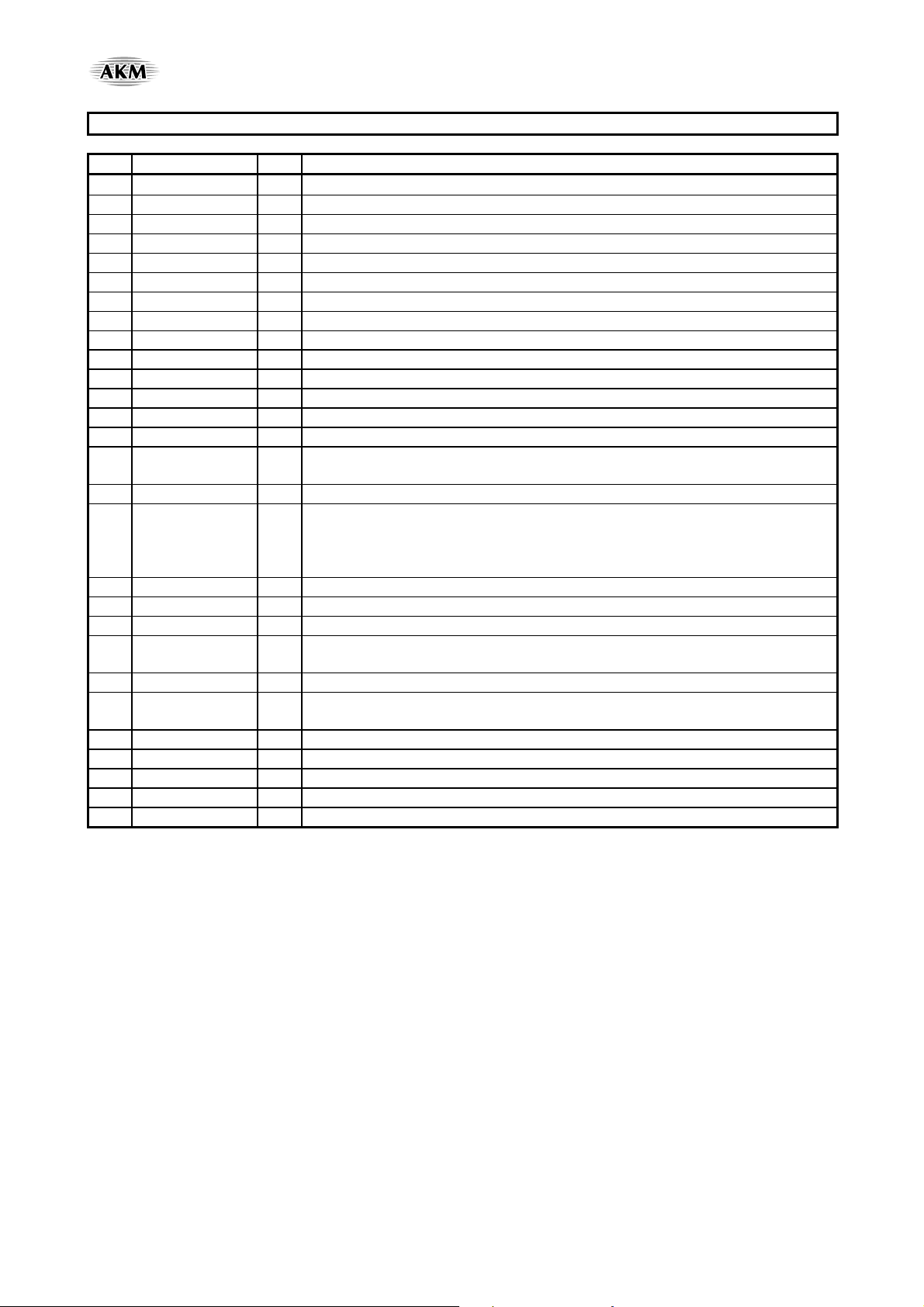
ABSOLUTE MAXIMUM RATINGS
(VSS1=VSS2=VSS3=VSS4=VSS1A=VSS2A=VSS3A=0V; Note 2, Note 3)
Parameter Symbol Min max Units
Power Supplies: CODEC Analog AVDD −0.3 4.0 V
(Note 4) PLLBT PVDD
−0.3 4.0 V
10bit SAR ADC SAVDD −0.3 4.0 V
CODEC Digital DVDD
−0.3 4.0 V
CODEC Digital I/O 2 TVDD2 −0.3 4.0 V
CODEC Digital I/O 3 TVDD3 −0.3 4.0 V
HP/SPK-Amp Analog AVDDA −0.3 6.0 V
HP/SPK-Amp Digital I/F TVDDA −0.3 6.0 V
Speaker-Amp & Headphone-Amp SVDDA −0.3 6.0 V
Charge Pump PVDDA
−0.3 4.0 V
Input Current, Any Pin Except Supplies IIN - ±10 mA
Analog Input Voltage 1 (Note 5)VINA1 −0.3 AVDD+0.3 V
Analog Input Voltage 2 (Note 6)VINA2 −0.3 SAVDD+0.3 V
Analog Input Voltage 3 (Note 7)VINA3 −0.3 (AVDDA+0.3) or 6.0 V
Analog Input Voltage 4 (Note 8)VINA4 −0.3 6.0 V
Digital Input Voltage 1 (Note 9) VIND1
−0.3 DVDD+0.3 V
Digital Input Voltage 2 (Note 10) VIND2
−0.3 TVDD2+0.3 V
Digital Input Voltage 3 (Note 11) VIND3
−0.3 TVDD3+0.3 V
Digital Input Voltage 4 (Note 12) VIND4
−0.3 (TVDDA+0.3) or 6.0 V
Ambient Temperature (powered applied) Ta −30 85 °C
Storage Temperature Tstg −65 150 °C
Ta=85ºC (Note 14) Pd1 - 0.91 WMaximum Power Dissipation
(Note 13) Ta=70ºC (Note 15) Pd2 - 1.18 W
Note 2. All voltages with respect to ground.
Note 3. VSS1, VSS2, VSS3, VSS4, VSS1A, VSS2A and VSS3A must be connected to the same analog
ground plane.
Note 4. TVDDA should be connected to DVDD.
Note 5. RIN4/IN4−, LIN4/IN4+, RIN3/IN3−, LIN3/IN3+, RIN2/IN2−, LIN2/IN2+, RIN1/IN1−, LIN1/IN1+ pins
Note 6. SAIN1, SAIN2, SAIN3 pins
Note 7. LIN1A, RIN1A, SPIN pins. The maximum value is smaller value between (AVDDA+0.3)V and 6.0V.
Note 8. VBATIN pin
Note 9. PDN, SCL, SDA, SDTI, LRCK, BICK, MCKI pins
Pull-up resistors at SDA and SCL pins should be connected to (DVDD+0.3)V or less voltage.
Note 10. BICKA, SYNCA, SDTIA pins
Note 11. BICKB, SYNCB, SDTIB pins
Note 12. PDNA, MCKIA pins. The maximum value is smaller value between (AVDDA+0.3)V and 6.0V.
Note 13. In case that the PCB wiring density is 300%. This power is the AK4675 internal dissipation that does not include
power of externally connected speaker and headphone.
Note 14. When Ta=85°C, the HP-Amp power must be under 30mW@16Ωand SPK-Amp power must be 1.0W@8Ω.
Note 15. When Ta=70°C, the HP-Amp power must be under 30mW@16Ωand SPK-Amp power must be 1.6W@8Ω.
WARNING: Operation at or beyond these limits may result in permanent damage to the device.
Normal operation is not guaranteed at these extremes.

[AK4675]
MS0963-E-00 2008/05
- 11 -
RECOMMENDED OPERATING CONDITIONS
(VSS1=VSS2=VSS3=VSS4=VSS1A=VSS2A=VSS3A=0V; Note 2)
Parameter Symbol min typ max Units
Power Supplies CODEC Analog AVDD 2.2 3.3 3.6 V
(Note 16) PLLBT PVDD 2.2 3.3 3.6 V
10bit SAR ADC SAVDD 2.2 3.3 3.6 V
CODEC Digital DVDD 1.6 3.3 3.6 V
CODEC Digital I/O 2 TVDD2 1.6 3.3 3.6 V
CODEC Digital I/O 3 TVDD3 1.6 3.3 3.6 V
HP/SPK-Amp Analog AVDDA 2.6 3.3 3.6 V
HP/SPK-Amp Digital I/F TVDDA 1.6 3.3 3.6 V
Speaker-Amp & Headphone-Amp SVDDA 3.0 3.6 5.5 V
Charge Pump PVDDA 2.6 3.3 3.6 V
Difference 1 AVDD−PVDD −0.1 0 +0.1 V
Difference 2 PVDDA–AVDDA −0.3 0 +0.3 V
Difference 3 SVDDA–AVDDA −0.3 - - V
Difference 4 DVDD–TVDDA
−0.3 0 +0.3 V
Note 2. All voltages with respect to ground.
Note 16. TVDDA must be connected to DVDD. The power-up sequence between AVDD, PVDD, SAVDD, DVDD,
TVDD2, TVDD3, AVDDA, TVDDA, SVDDA and PVDDA is not critical. However, the PDN and PDNA pin
must be held to “L” until all power supply pins are supplied. After all power supplies are filled, PDN and PDNA
pins should be set to “H”.
* The AK4675 supports the following two cases of partial power ON/OFF. In these cases, PDNA pin should be “L” and
all power management bits (PMVCM, PMMP, PMMICL, PMMICR, PMADL, PMADR, PMDAL, PMDAR, PMPLL,
PMLOOPL, PMLOOPR, PMAINL1, PMAINR1, PMAINL2, PMAINR2, PMAINL3, PMAINR3, PMAINL4,
PMAINR4, PMLO1, PMRO1, PMLO2S, PMRO2S, PMLO3, PMRO3, PMSRA, PMSRB, PMPCM, and PMSAD)
should be OFF or PDN and PDNA pins should be “L”.
1. DVDD=TVDDA=SVDDA=ON, AVDD=PVDD=SAVDD=TVDD2=TVDD3=AVDDA=PVDDA=OFF
2. DVDD=TVDDA=ON, AVDD=PVDD=SAVDD=TVDD2=TVDD3=AVDDA=PVDDA=SVDDA=OFF
When the power state is changed from OFF to ON in the above cases, the PDN and PDNA pins should be set to “H” after
all power supply pins are supplied.
When DVDD and TVDDA are powered OFF, AVDD, PVDD, SAVDD, TVDD2, TVDD3, AVDDA, TVDDA, SVDDA
or PVDDA must be powered OFF. When only DVDD and TVDDA are OFF, leak current of 10mA to 100mA may occur.
* AKEMD assumes no responsibility for the usage beyond the conditions in this datasheet.

[AK4675]
MS0963-E-00 2008/05
- 12 -
ANALOG CHARACTERISTICS (CODEC)
(Ta=25°C; AVDD=PVDD=SAVDD=DVDD=TVDD2=TVDD3=AVDDA=PVDDA=TVDDA=3.3V, SVDDA=3.6V;
VSS1=VSS2=VSS3=VSS4=VSS1A=VSS2A=VSS3A=0V; Signal Frequency=1kHz; 16bit Data; fs=44.1kHz,
BICK=64fs, LP bit = “0”; Measurement frequency=20Hz ∼20kHz; unless otherwise specified)
Parameter min typ max Units
MIC Amplifier: LIN1/RIN1/LIN2/RIN2/LIN3/RIN3/LIN4/RIN4 pins; PMAINL1/R1/L2/R2/L3/R3/L4/R4 bits = “0”
Input Resistance
MGNL/R0 bit = “0” 28 42 56 kΩ
MGNL/R0 bit = “1” 20 30 40 kΩ
Gain (Note 17)
Max (MGNL/R3-0 bits = “FH”) - +30 - dB
Min (MGNL/R3-0 bits = “1H”) - −12 - dB
MIC Power Supply: MPWR pin
Output Voltage (Note 18) 2.47 2.64 2.81 V
Load Resistance 0.5 - - kΩ
Load Capacitance - - 30 pF
MIC Detection: MDT pin
Comparator Voltage Level (Note 19) 0.165 0.247 mV
Internal pull down Resistance 250 500 750 kΩ
Stereo ADC Analog Input Characteristics:
LIN1/RIN1/LIN2/RIN2/LIN3/RIN3/LIN4/RIN4 pins →Stereo ADC →IVOL, IVOL=0dB, ALC=OFF
Resolution - - 16 Bits
(Note 21) 0.150 0.176 0.203 Vpp
Input Voltage (Note 20) (Note 22) 1.68 1.98 2.28 Vpp
(Note 21) 72 82 - dB
S/(N+D) (−1dBFS) (Note 22) - 87 - dB
(Note 21) 75 86 - dB
D-Range (−60dBFS, A-weighted) (Note 22) - 95 - dB
(Note 21) 75 86 - dB
S/N (A-weighted) (Note 22) - 95 - dB
(Note 21) 75 90 - dB
Interchannel Isolation (Note 22) - 100 - dB
(Note 21) - 0.1 0.8 dB
Interchannel Gain Mismatch (Note 22) - 0.1 0.8 dB
Note 17. In case of full-differential input, MGAIN=0dB (min) and AVDD=2.4V (min).
Note 18. Output voltage is proportional to AVDD voltage. Vout = 0.8 x AVDD (typ).
Note 19. Comparator Voltage Level is proportional to AVDD voltage. Vth = 0.05 x AVDD(min), 0.075 x AVDD(max).
Note 20. Input voltage is proportional to AVDD voltage. Vin = 0.053 x AVDD (typ)@MGNL3-0=MGNR3-0 bits =
“CH” (+21dB), Vin = 0.6 x AVDD(typ)@MGNL3-0=MGNR3-0 bits = “5H” (0dB).
Note 21. MGNL3-0=MGNR3-0 bits = “CH” (+21dB).
Note 22. MGNL3-0=MGNR3-0 bits = “5H” (0dB).

[AK4675]
MS0963-E-00 2008/05
- 13 -
Parameter min typ max Units
Stereo DAC Characteristics:
Resolution - - 16 Bits
Stereo Line Output Characteristics:
Stereo DAC →LOUT1/ROUT1/LOUT3/ROUT3 pins, ALC=OFF, IVOL=0dB, OVOL=0dB, L1VL=L3VL=0dB,
RCV bit = “0”, RL=10kΩ; unless otherwise specified.
Output Voltage (Note 23) 1.78 1.98 2.18 Vpp
S/(N+D) (0dBFS) 75 85 - dB
S/N (A-weighted) 82 92 - dB
Interchannel Isolation 85 100 - dB
Interchannel Gain Mismatch - 0.1 0.5 dB
Load Resistance 10 - - kΩ
Load Capacitance - - 30 pF
Stereo Line Output Characteristics:
Stereo DAC →LOUT2S/ROUT2S pins, ALC=OFF, IVOL=0dB, OVOL=0dB, RL=25kΩ; unless otherwise specified.
Output Voltage (Note 23) 1.78 1.98 2.18 Vpp
S/(N+D) (0dBFS) 72 85 - dB
S/N (A-weighted) 82 92 - dB
Interchannel Isolation 85 100 - dB
Interchannel Gain Mismatch - 0.1 0.5 dB
Load Resistance 25 - - kΩ
Load Capacitance - - 30 pF
Mono Receiver-Amp Output Characteristics:
Stereo DAC →RCP/RCN pins, ALC=OFF, IVOL=0dB, OVOL=0dB, L1VL=0dB, RCV bit = “1”, RL=32Ω, BTL;
unless otherwise specified.
Output Voltage (Note 24)
−6dBFS, RL=32Ω(Po=15mW) 1.57 1.96 2.35 Vpp
−3dBFS, RL=32Ω(Po=30mW) - 2.77 - Vpp
S/(N+D)
−6dBFS, RL=32Ω(Po=15mW) 40 60 - dB
−3dBFS, RL=32Ω(Po=30mW) - 20 - dB
S/N (A-weighted) 82 92 - dB
Load Resistance 32 - - Ω
Load Capacitance - - 30 pF
Note 23. The Output voltage is proportional to the AVDD voltage. Vout = 0.6 x AVDD (typ).
Note 24. The Output voltage is proportional to the AVDD voltage. Vout = (RCP) −(RCN) = 0.59 x AVDD
(typ)@−6dBFS.
Note 25. VSS1 load capacitance to output pins.

[AK4675]
MS0963-E-00 2008/05
- 14 -
Parameter min typ max Units
Mono Line Output Characteristics: Stereo DAC →LOP/LON pins, ALC=OFF, IVOL=0dB, OVOL=0dB,
L3VL=0dB, LODIF bit = “1”, RL=10kΩfor each pin (Full-differential)
Output Voltage (Note 26) 3.52 3.96 4.36 Vpp
S/(N+D) (0dBFS) 75 85 - dB
S/N (A-weighted) 85 95 - dB
Load Resistance (LOP/LON pins, respectively) 10 - - kΩ
Load Capacitance (LOP/LON pins, respectively) - - 30 pF
Single-ended Line Input: LIN1/RIN1/LIN2/RIN2/LIN3/RIN3/LIN4/RIN4 pins;
(MDIF1=MDIF2=MDIF3=MDIF4 bits = “0”)
Maximum Input Voltage (Note 28) - 1.98 - Vpp
Gain
InputåLOUT1/ROUT1/LOUT2S/ROUT2S/LOUT3/ROUT3 (LODIF=RCV bits = “0”)
−1 0 +1 dB
Input åRCP/RCN/LOP/LON (LODIF=RCV bits = “1”)
- +6 - dB
Full-differential Line Input: IN1+/−, IN2+/−, IN3+/−, IN4+/−pins;
(MDIF1=MDIF2=MDIF3=MDIF4 bits = “1”)
Maximum Input Voltage (Note 29) - 1.98 - Vpp
Gain
InputåLOUT1/ROUT1/LOUT2S/ROUT2S/LOUT3/ROUT3 (LODIF=RCV bits = “0”)
−1 0 +1 dB
Input åRCP/RCN/LOP/LON (LODIF=RCV bits = “1”, Note 30)
- +6 - dB
Note 26. The Output voltage is proportional to the AVDD voltage. Vout = (LOP) −(LON) = 1.2 x AVDD (typ).
Note 27. VSS1 load capacitance to output pins.
Note 28. The Maximum Input voltage is proportional to the AVDD voltage. Vin = 0.6 x AVDD (typ).
Note 29. The Maximum Input voltage is proportional to the AVDD voltage. Vin = (IN4+) −(IN4−) = 0.6 x AVDD (typ).
Note 30. Vout = (RCP) −(RCN) at RCV bit = “1”, Vout = (LOP) −(LON) at LODIF bit = “1”.

[AK4675]
MS0963-E-00 2008/05
- 15 -
ANALOG CHARACTERISTICS (HP/SPK-Amp)
(Ta=25°C; AVDD=PVDD=SAVDD=DVDD=TVDD2=TVDD3=AVDDA=PVDDA=TVDDA=3.3V, SVDDA=3.6V;
VSS1=VSS2=VSS3=VSS4=VSS1A=VSS2A=VSS3A=0V; Input Signal Frequency =1kHz; Measurement band
width=10Hz ∼20kHz; Headphone-Amp: RL =16Ω; Speaker-Amp: RL =8Ω+ 10μH; Charge Pump Circuit External
Capacitance: C1=C2= 2.2μF (Figure 3); unless otherwise specified)
Parameter min typ max Units
LIN1A, RIN1A pins
Input Resistance 25 50 110 kΩ
Input Analog Volume: L1V3-0, R1V3-0 bits
Step Size 1 2 3 dB
Gain Control Range −20 - +10 dB
Headphone-Amp: (LIN1A/RIN1A åHPL/HPR pins), HPGA = 0dB
Output Power (THD+N=1%) SVDDA=3.3V - 64 - mW
THD+N 0.7Vrms Single-ended Input, Po = 30mW - -58 - dB
Output Noise (A-weighted) - 24 40 μVrms
Interchannel Gain Mismatch - 0.2 0.8 dB
Load Resistance 16 - - Ω
Load Capacitance - - 300 pF
Output Voltage: 0.7Vrms at single-ended Input 0.62 0.69 0.76 Vrms
PSRR
217Hz (Note 31)
1kHz (Note 31)
217Hz (Note 32)
1kHz (Note 32)
-
-
-
-
70
70
100
80
-
-
-
-
dB
dB
dB
dB
Interchannel Isolation 60 80 - dB
Headphone Analog Volume 1 (HPGA4-0 bits)
Step Size 0.5 2 3.5 dB
Gain Control Range −50 - +12 dB
SPIN pins
Input Resistance 15 26 36 kΩ
Speaker Analog Volume: SPGA5-0 bits
Step Size 0.1 0.5 0.9 dB
Gain Control Range −12 - +19.5 dB
Class-D Speaker-Amp: SPIN åSPP/SPN; ALC = OFF, Input Volume=SPGA=0dB, BTL
Output Power (THD+N=10%)
SVDDA=5.0V
SVDDA=3.6V
-
-
1.6
0.8
-
-
W
W
Output Level (Note 33)
SVDDA = 5.0V, Input Level = 0.85Vrms
SVDDA = 3.6V, Input Level = 0.64Vrms
SVDDA = 3.6V, Input Level = 0.46Vrms
-
-
1.33
2.7
2.0
1.48
-
-
1.63
Vrms
Vrms
Vrms
THD+N: Po=0.25W, Input Level=0.46Vrms(Note 33) - -65 -40 dB
Output Noise (A-weighted) - 71 150 μVrms
Load Resistance 8 - - Ω
Load Capacitance (Note 34) - - 300 pF
PSRR
217Hz (Note 35)
1kHz (Note 35)
217Hz (Note 36)
1kHz (Note 36)
-
-
-
-
60
50
50
50
-
-
-
-
dB
dB
dB
dB
Switching Frequency 150 250 400 kHz
Short Protection Current (Note 37) 40 120 mA
Start-Up Time 18 30 48 ms

[AK4675]
MS0963-E-00 2008/05
- 16 -
Note 31. PSR is applied to AVDDA and PVDDA with 100mVpp. This is the value of convoluting sinusoidal voltage of
100mVpp.
Note 32. PSR is applied to SVDDA with 0.89Vpp. This is the value of convoluting sinusoidal voltage of 100mVpp.
Note 33. When the input data is single-ended.
Note 34. VSS1 load capacitance to output pins. For differential signals, the load capacitance will be twice as big as this
value.
Note 35. PSR is applied to AVDDA with 100mVpp. This is the value of convoluting sinusoidal voltage of 100mVpp.
Note 36. PSR is applied to SVDDA with 100mVpp. This is the value of convoluting sinusoidal voltage of 100mVpp.
Note 37. The average current between SVDDA and VSS2A, when the SPP pin and SPN pin are shorted and 1kHz,
0.85Vrms sine wave is input at Single-ended mode.
PVEE pin
Charge Pump Circuit CN pin
C2
CP pin
Headphone-amp negative voltage
C1
VSS3A
Figure 3. Charge Pump Circuit External Capacitor
Parameter min typ max Units
Battery Monitor: (BATCPU bit = “1”)
Input Resistance (VBATIN pin) 5 10 - kΩ
Attenuation (VBATO / VBATIN) (Note 38) 0.245 0.25 0.255 -
Note 38. When input 4.4V to the VBATIN pin.

[AK4675]
MS0963-E-00 2008/05
- 17 -
ANALOG CHARACTERISTICS (Power Supply Current)
(Ta=25°C; AVDD=PVDD=SAVDD=DVDD=TVDD2=TVDD3=AVDDA=PVDDA=TVDDA=3.3V, SVDDA=3.6V;
VSS1=VSS2=VSS3=VSS4=VSS1A=VSS2A=VSS3A=0V;
Signal Frequency=1kHz; 16bit Data; fs=44.1kHz, BICK=64fs, LP bit = “0”; Measurement frequency=20Hz ∼20kHz;
Headphone-Amp: RL =16Ω; Speaker-Amp: RL =8Ω+ 10μH; Charge Pump Circuit External Capacitance: C1=C2=2.2μF
(Figure 3); unless otherwise specified)
Parameter min typ max Units
Power Supplies:
CODEC Block Power Up (PDN pin = “H”, All Circuits Power-up)
(Note 39) - 20 - mA
(Note 40) - 21 30 mA
AVDD+PVDD+DVDD
+TVDD2+TVDD3+SAVDD (Note 41) - 8 12 mA
HP/SPK-Amp Block Power Up (PDNA pin = “H”, All Circuits Power-up)
AVDDA+TVDDA: ALL ON (Note 42) - 4.0 6.5 mA
HP-Amp ON (Note 43) - 2.0 - mA
SPK-Amp ON (Note 44) - 2.8 - mA
PVDDA (No Output) HP-Amp ON - 1.3 3.2 mA
SVDDA (No Output): HP-Amp ON - 2.0 4.0 mA
SPK-Amp ON 1.0 4.0 mA
Power Down (PDN=PDNA pins = “L”) (Note 45)
AVDD+PVDD+DVDD+TVDD2+TVDD3+SAVD
D+ AVDDA+PVDDA+SVDDA+TVDDA - 1 60
μA
Note 39. EXT Slave Mode and LP bit = “0”, fs=44.1kHz, PMMICL = PMMICR = PMADL = PMADR = PMDAL =
PMDAR = PMLO1 = PMRO1 = PMLO2S = PMRO2S = PMLO3 = PMRO3 =PMSAD = PMVCM bits = “1”,
PMPLL = MCKO = PMMP = M/S = PMSRA = PMSRB = PMPCM bits = “0”.
AVDD=12.1mA (typ), PVDD=0mA (typ), DVDD=5.6mA (typ), TVDD2=0mA (typ), TVDD3=0mA (typ),
SAVDD=0.8mA (typ).
Note 40. PLL Master Mode and LP bit = “0”, fs=44.1kHz, PMADL = PMMICL= PMMICR= PMADR = PMDAL =
PMDAR = PMLO1 = PMRO1 = PMLO2S = PMRO2S = PMLO3 = PMRO3 =PMSAD = PMVCM = PMPLL =
M/S = PMMP bits = “1”, MCKO = PMSRA = PMSRB = PMPCM bits = “0”, MCKI=11.2896MHz.
AVDD=TBDmA (typ), PVDD=TBDmA (typ), DVDD=TBDmA (typ), TVDD2=TBDmA (typ),
TVDD3=TBDmA (typ), SAVDD=TBDmA (typ).
Note 41. EXT Slave Mode and LP bit = “1”, fs=8kHz, PMVCM = PMMP = PMMICL = PMADL = PMDAL = RCV =
PMLO1 = PMRO1 = PMSRA = PMSRB = PMPCM = “1”.
AVDD=3.2mA (typ), PVDD=0.8mA (typ), DVDD=2.7mA (typ), TVDD2=0mA (typ), TVDD3=0mA (typ),
SAVDD=0mA (typ).
Note 42. Headphone-Amp & Speaker-Amp are powered-up.
(PMVCMA=PMOSC=PMCP=PMHPL=PMHPR=PMMHL=PMMHR=PMSPK=PMV1 bits= “1”)
Note 43. Headphone-Amp is powered-up.
(PMVCMA=PMOSC=PMCP=PMHPL=PMHPR=PMMHL=PMMHR=PMV1 bits= “1”,
PMSPK bits= “0”)
Note 44. Speaker-Amp is powered-up
(PMVCMA=PMOSC=PMCP=PMSPK bits= “1”,
PMHPL=PMHPR=PMMHL=PMMHR=PMV1 bits= “0”)
Note 45. All digital input pins are fixed to each supply pin (DVDD, TVDD2 or TVDD3) or VSS4.

[AK4675]
MS0963-E-00 2008/05
- 18 -
SRC CHARACTERISTICS
(Ta=25°C; AVDD=PVDD=SAVDD=DVDD=TVDD2=TVDD3=3.3V; VSS1=VSS2=VSS3=VSS4=0V;
Signal Frequency=1kHz; 16bit Data; Measurement frequency=20Hz ∼3.4kHz; unless otherwise specified)
Parameter Symbol min typ max Units
SRC Characteristics (Down Sampling: SRC-A): SDTI åSRC-A åSDTOA/SDTOB
Resolution - - 16 Bits
Input Sample Rate (Note 47) FSI (fs) 8 - 48 kHz
Output Sample Rate (Note 47) FSO (fs2) - 8 - kHz
THD+N (Input = 1kHz, −1dBFS, Note 46)
FSO/FSI = 8kHz/44.1kHz - -94 - dB
Dynamic Range (Input = 1kHz, −60dBFS, Note 46)
FSO/FSI = 8kHz/44.1kHz - 97 - dB
Ratio between Input and Output Sample Rate FSO/FSI 1/6 - 1 -
SRC Characteristics (Up Sampling: SRC-B): SDTIA/SDTIB åSRC-B åSDTO
Resolution - - 16 Bits
Input Sample Rate (Note 47) FSI (fs2) - 8 - kHz
Output Sample Rate (Note 47) FSO (fs) 8 - 48 kHz
THD+N (Input = 1kHz, −1dBFS, Note 46)
FSO/FSI = 44.1kHz/8kHz - -95 - dB
Dynamic Range (Input = 1kHz, −60dBFS, Note 46)
FSO/FSI = 44.1kHz/8kHz - 100 - dB
Ratio between Input and Output Sample Rate FSO/FSI 1 - 6 -
Note 46. Measured by Audio Precision System Two Cascade.
Note 47. “fs” is the sampling frequency for Stereo CODEC. “fs2” is for PCM I/F.

[AK4675]
MS0963-E-00 2008/05
- 19 -
ANALOG CHARACTERISTICS (10bit SAR ADC)
(Ta=25°C; AVDD=PVDD=SAVDD=DVDD=TVDD2=TVDD3=3.3V; VSS1=VSS2=VSS3=VSS4=0V; unless
otherwise specified)
Parameter min typ max Units
10bit SAR ADC Characteristics
Resolution - 10 - Bits
No Missing Codes 9 10 - Bits
Integral Linearity Error - - ±2 LSB
DNL -
±1 - LSB
Analog Input Voltage Range 0 - SAVDD V
Offset Error - - ±3 LSB
Gain Error - - ±2 LSB
Accuracy (Note 48) - -
±1 %
Note 48. Accuracy is the difference between the output code when 1.1V is input to SAIN1, SAIN2 or SAIN3 pin and the
“ideal” code at 1.1V.

[AK4675]
MS0963-E-00 2008/05
- 20 -
FILTER CHARACTERISTICS (CODEC)
(Ta=25°C; AVDD=PVDD=SAVDD=2.2 ∼3.6V; DVDD=TVDD2=TVDD3=1.6 ∼3.6V; fs=44.1kHz; Programmable
Filter=OFF)
Parameter Symbol min typ max Units
ADC Digital Filter (Decimation LPF):
Passband (Note 49) ±0.16dB PB 0 - 17.3 kHz
−0.66dB - 19.4 - kHz
−1.1dB - 19.9 - kHz
−6.9dB - 22.1 - kHz
Stopband SB 25.9 - - kHz
Passband Ripple PR - - ±0.1 dB
Stopband Attenuation SA 69 - - dB
Group Delay (Note 50) GD - 19 - 1/fs
Group Delay Distortion ΔGD - 0 -
μs
DAC Digital Filter (LPF):
Passband (Note 49) ±0.1dB PB 0 - 17.4 kHz
−1.0dB - 20.0 - kHz
−3.0dB - 21.1 - kHz
Stopband SB 25.7 - - kHz
Passband Ripple PR - - ±0.1 dB
Stopband Attenuation SA 68 - - dB
Group Delay (Note 50) GD - 19 - 1/fs
DAC Digital Filter (LPF) + SCF:
Frequency Response: 0 ∼20.0kHz FR -
±1.4 - dB
Note 49. The passband and stopband frequencies scale with fs (system sampling rate).
For example, DAC is PB=0.454 x fs (@−0.7dB). Each response refers to that of 1kHz.
Note 50. The calculated delay time caused by digital filtering. This time is from the input of analog signal to setting of the
16-bit data of both channels from the input register to the output register of the ADC.
For the DAC, this time is from setting the 16-bit data of both channels from the input register to the output of
analog signal.
Table of contents
Other AKM Conference System manuals
Popular Conference System manuals by other brands

ICM Controls
ICM Controls IG-02 Operating instruction

Ocean Reef
Ocean Reef GAMMA-ALPHA 2010 owner's manual

Samsung
Samsung SyncMaster VC240 reference guide

Lars Thrane
Lars Thrane Iridium Certus 200 User & installation manual

CommScope
CommScope OneCell RP Series Installation

ADTRAN
ADTRAN NetVanta 7100 IP PBX Configuration guide