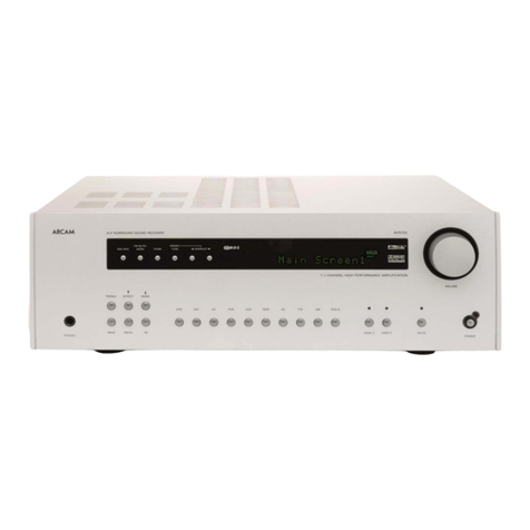
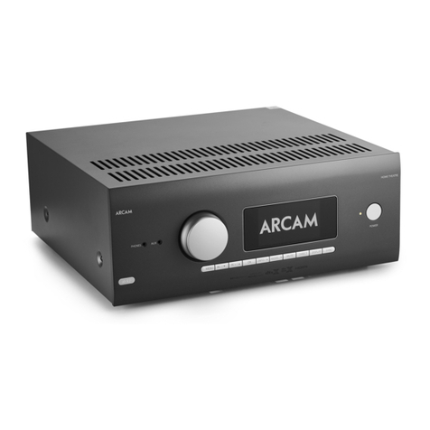
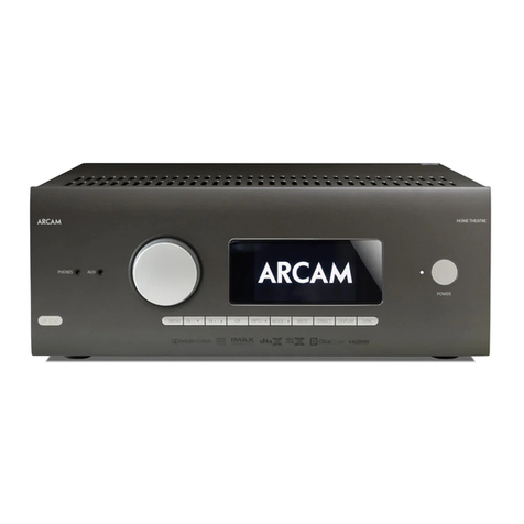
Arcam AVR600 User manual

UA
AVR600 Service manual issue 1.2
ARCAM

This PCB provides the power for the unit through CON203:
+5V_STBY – 5V standby supply L118 RS232, L126 display (on in standby)
+3V3 PW338 – L122 PW338 supply (on in standby)
1V8D – L122 PW338 supply (on in standby)
+5V_1 – general 5V supply
+6V_1 – L156 DSP, L126 Display & L119 NET supply
+40V_VFD – L126 Display
+15V – linear +15V supply
-15V – linear -15V supply
LK100 or the thermal switch from the power amp transformer is required to
pass the live mains. SW101 switches between 230V & 115V.
R101 & R102 are NTC parts to prevent inrush currents when the power amp
is turned on.
CON202 takes the Clk PSU sync signal from L121, Relay SW from L122 (to
turn on the main supplies) and /AC present back to L122. /AC present is
generated from the standby transformer secondaries with D200.D210 &
TR200. This will prevent the unit from starting if it is not low.
The standby transformer is rectified with DBR200 (GBU4K) to give
UNREG_PW338 which is used for the 1V8D (REG206 – LM2670),
3V3_PW338 (REG201 – LM2670). The 12V for the relays to switch the
secondaries are also generated from REG207 (LM7812) which is then
regulated down to give +5V_STBY REG200 (LM7805).
When the signal Relay SW is taken high by the PW338, the secondaries of
the system & power amp transformer are switched in (RLY101 & RLY102).
This enables +15V, -15V (REG204 & REG205) & +5V_1 & +6V_1 (REG202 &
REG203).
L123AY– Connection board and PSU

This PCB selects between one of five component video inputs & also provides
the output connector for Zone 3 audio.
IC100, IC101 & IC104 (LT1675CGN video buffers) require +5V & -5V. The
+5V comes direct from L123 & -5V is generated locally from the -15V supply
(from L123).
Selection of the five inputs is via IC102 (74HCT595D serial to parallel
converter, controlled via SPI Clk, Data & Vcomp latch) and IC100, IC101,
IC104. IC102 generates a /ENx signal which tri-states the output when high
and enables the output when low. When low the input is selected with the
SELx signal, high for input1, low for input2.
Truth table:
EN0 SEL0 EN1 SEL1 EN2 SEL2
0 0 1 X 1 x SAT
0 1 1 X 1 x AV
1 x 0 0 1 x VCR
1 x 0 1 1 x DVD
1 x 1 x 0 1 PVR
1 x 1 x 1 x BLANK*
*When component input is not used, BLANK should be selected.
SKT101 provides zone 3 audio output.
L113AY Component Input – Output board

This PCB selects between one of five s-video & composite video inputs for the
main input & zone 2 video. It also controls the volume control for Zone 2 & 3.
The main input video is selected using IC200 (LA73031V video mux) under
the control of IC205 & IC208 (74HC595 serial to parallel converters, controlled
by SPI Clk, Data & Vid IO Mux Latch). Inputs are selected using INSEL1,
INSEL2, INSEL3 (Z2 INSEL1, Z2INSEL2, Z2INSEL3 for Zone 2 via IC203 –
LA73031V video mux).
As there is only one sync separator within each LA73031V, it is necessary to
select if this is used for S-video or composite (this means that once composite
video is selected as the source, it is not possible to autodetect S-video) -
SYNC CTL selects, low = Svideo, high = composite.
There are two buffered (IC201 & IC202 – BA7623F video buffers) tape
outputs, VCR & PVR which can be muted with VCR Mute & PVR Mute
respectively through a transistor network. Each output is muted when that
input is selected to prevent feedback, otherwise the output is a copy of the
composite or S-video signal going to the main zone.
Zone 2 video is buffered through IC204 (BA7623F video buffer) and can also
be mute, if required using the signal Z2Vid Mute & a transistor network.
When S-video or composite inputs are not used, V MUX STBY should be
asserted high. Note: this will disable both the main Zone & Zone 2 S-video &
composite muxes.
Video Input Truth table:
(Z2)INSEL1 (Z2)INSEL2 (Z2)INSEL3 (Z2)SYNCCTL
0 0 0 1 AV comp
0 0 1 1 SAT comp
0 1 0 1 DVD comp
0 1 1 1 PVR comp
1 0 0 1 VCR comp
0 0 0 0 AV S-vid
0 0 1 0 SAT S-vid
0 1 0 0 DVD S-vid
0 1 1 0 PVR S-vid
1 0 0 0 VCR S-vid
Volume control for Zone 2 & 3 uses IC300 & IC301 (BD3812F volume
controls) via a two-wire interface (Zone SPI Clk & Zone SPI Data). IC300 has
address D2, D1=1, IC301 has address D2, D1=0. The volume controls can
be muted from IC208 (Serial to parallel converter) using Z2 vol mute or Z3 vol
mute. The outputs are also relay controlled for powerup/down with Z2 Mute &
Z3 Mute directly from the PW338 using RLY300 & RLY301 as shunt relays.
The +7VA & -7VA required for the BD3812F volume controls is derived using
REG300 (LM1117) & REG301 (LM337LZ) from the +15V & -15V from L123.
L114AY – Video input – output

This PCB selects on of 8 external digital inputs or one of two internal digital
inputs & generates BClk, WClk & MClk for the DSP (see L156) & DAC (see
L117). It also generates the clocks for the ADC (see L116) when the unit is in
ADC mode.
The CD, AV & DVD inputs use coaxial connector SKT100 and feed into IC200
& IC201 (DS9637ACM buffers). The Tape, SAT, VCR & PVR inputs use
optical connectors RX100, RX101, RX102, RX103. The outputs are padded
down to give 3v3 outputs. There is also the Aux input which can be selected
(see L117), the Net input (see L119) and the HDMI SPDIF (see L122).
One of these inputs is then selected using IC202 & IC203 (74HC151 8-1 mux)
under the control of IC204 (74HC595D serial to parallel converter) controlled
by AN SPI Clk, AN SPI Data & Dig Mux Latch.
The selected input is fed to IC100 (WM8805 SPDIF Rx/Tx) which is controlled
from the PW338 via AN SCL, AN SDA & SPDIF /RESET. IC100 generates
8805MClk, 8805BClk & 8805WClk. Also, SPDIF Out which is a de-jittered
SPDIF stream which is then buffered by IC103 part A, B, C & D (parts E & F
are unused) to give both the optical output (TXC100) & 75ohmcoaxial output
(SKT101).
The selected input is also fed to IC205 part A (74HC123D monostable, part B
unused) which gives a high output from pin 13 (SPDIF_PRESENT to the
PW338) if an SPDIF signal is present.
BClk=64* WClk
MClk=128*WClk (192kHz/176.4kHz), 256*WClk (96kHz/88.2kHz), 512*WClk
(48kHz/44.1kHz) – this clock is used by the PSU to synchronise the switchers.
IC105 (XC95C36 Xilinx) generates a pre-delayed SPDIF stream from the
HDMI clocks (only MClk & WClk used) as the HDMI SPDIF is turned off
during HD audio transfer & the WM8805 does not have a zero delay PLL.
IC104 (74HCT157 Quad 2-1 mux) can also be used to re-direct the clocks
from the HDMI into the system.
IC100 (WM8805) can also operate in master mode to generate clocks for the
ADC when processing an analogue input.
3V3D is generated locally on the PCB from 5V_1 using REG200 (LM1117).
L115AY Digital Input – Output board

This PCB selects the analogue input for the main zone & Zone 2/3 and also
digitises the analogue input for processing by the DSP / transmission over
SPDIF.
One of seven phono inputs (Tape, CD, AV, DVD, SAT, VCR, PVR), Aux
(external) input (see L127), AM/FM & DAB(internal)/Sirius(external) inputs
(see L118), Net (internal) input (see L119) and Phono (see L117).
The input for the main zone is selected using IC200, IC208, IC205, IC209
(74HC4051D 8-1 mux) under the control of IC101 & IC102 (74HC595 serial to
parallel converter), controlled by AN SPI Data, AN SPI Clk & A In Mux Latch.
The muxes operate on the virtual earth of IC203 part A (left channel) & IC206
part A (right channel), both NJM2114 op amps, inverting the signal. Part B of
these two op amps re-invert the signal (correct phase) and this output is used
by the ADC & the direct path – Main L & Main R.
IC202 (NJM2114 op amp) inverts the original output of the mux (correct
phase) to provide the three tape outputs, Tape Out, PVR Out & VCR Out.
Each of these has individual mutes – IC201, IC204, IC207 (DG413DY
analogue mux) which mutes the output if that input is selected to prevent
feedback. Otherwise, the output is the selected input. The signals for these
mutes, /Tape Mute, /PVR Mute, /VCR Mute come from IC102 (74HC595
serial – parallel converter).
Selection of the Zone 2 input is very similar, using IC300, IC303, IC302,
IC304 (74HC4051 8-1 muxes) and IC301 (NJM2114 op amp).
The Main L & Main R are connected to input AIN1A/AIN1B of IC100 (CS5345
ADC). Aux L & Aux R are also connected to AIN4A/AIN4B as this is
configurable as the MIC input and can provide power from pin25 of IC100.
the ADC is controlled from the PW338 via AN SCL & AN SDA. ADC/RESET
also comes from IC102, so the ADC can be held in reset when not being
used.
The ADC always operates in slave mode and will sample at the rate dictated
by the incoming clocks from L115 (buffered on L122). ADC Data is sent to
L115 so that it can be transmitted by the SPDIF transmitter and selected for
input to the DSP.
+12VA (REG301 LM7812) & -12VA (REG304 LM7912) for the local op amps
are derived from +15V & -15V from L123.
+5VA (used by the ADC) is derived from the +12VA with REG302 (LM1117).
+3V3D (used by the ADC) is derived from the +12VA with REG300 (LM1117).
+3V3A (REG303 LM1117) & -3V3A (REG305 LM337LZ) for the muxes are
derived from +5VA & -12VA.
L116AY Analogue input board
Truth table
MUTE Main Asel Z2 Asel
ADC
/RST VCR PVR TAPE 5 4 3 2 1 0 5 4 3 2 1 0
x x x x x x x x x x 1 1 1 0 0 0 Z2 CD
x x x x x x x x x x 1 1 1 0 0 1 Z2 AV
x x x x x x x x x x 1 1 1 0 1 0 Z2 SAT
x x x x x x x x x x 1 1 1 0 1 1 Z2 DVD
x x x x x x x x x x 1 1 1 1 0 0 Z2 VCR
x x x x x x x x x x 1 1 1 1 0 1 Z2 PVR
x x x x x x x x x x 1 1 1 1 1 0 Z2 TAPE
x x x x x x x x x x 0 0 0 1 1 1 Z2 Phono
x x x x x x x x x x 0 0 1 1 1 1 Z2 Aux
x x x x x x x x x x 0 1 0 1 1 1 Z2 GND
x x x x x x x x x x 0 1 1 1 1 1 Z2 AM/FM
x x x x x x x x x x 1 0 0 1 1 1 Z2 DAB/Sirius
x x x x x x x x x x 1 0 1 1 1 1 Z2 Net
x x x x x x x x x x 1 1 0 1 1 1 Z2 Spare
x x x x x x x x x x 1 1 1 1 1 1 Z2 GND
x x x x 1 1 1 0 0 0 x x x x x x Main CD
x x x x 1 1 1 0 0 1 x x x x x x Main AV
x x x x 1 1 1 0 1 0 x x x x x x Main SAT
x x x x 1 1 1 0 1 1 x x x x x x Main DVD
x x x x 1 1 1 1 0 0 x x x x x x Main VCR
x x x x 1 1 1 1 0 1 x x x x x x Main PVR
x x x x 1 1 1 1 1 0 x x x x x x Main Tape
x x x x 0 0 0 1 1 1 x x x x x x Main Phono
x x x x 0 0 1 1 1 1 x x x x x x Main Aux
x x x x 0 1 0 1 1 1 x x x x x x Main GND
x x x x 0 1 1 1 1 1 x x x x x x Main AM/FM
x x x x 1 0 0 1 1 1 x x x x x x Main DAB/Sirius
x x x x 1 0 1 1 1 1 x x x x x x Main Net
x x x x 1 1 0 1 1 1 x x x x x x Main Spare
x x x x 1 1 1 1 1 1 x x x x x x Main GND
x 1 1 0 x x x x x x x x x x x x Tape out mute
x 1 0 1 x x x x x x x x x x x x PVR out mute
x 0 1 1 x x x x x x x x x x x x VCR out mute
x 1 1 1 x x x x x x x x x x x x No loop mute
0 x x x x x x x x x x x x x x x ADC reset
1 x x x x x x x x x x x x x x x ADC running

This PCB converts the digital audio from the DSP (see L156) to analogue
audio. It also configures the use of channels 6 & 7, has the headphone amp,
has the RIAA equaliser for the Phono input and handles the multi-channel
analogue input.
The phono amplifier is a standard RIAA response and is intended for use with
MM cartridges, 5mV (check this!) output. C128 & C129 are important to
prevent the DC offset of IC100 (NJM2114 op amp) from causing problems.
IC101 forms the basis of the headphone amplifier. The output of this section
goes to L127.
IC300 (CS4385 8-channel DAC) takes multichannel data (Data LR, Data
CSw, Data SlSr, Data SblSbr) from the DSP (L156) in addition to clocks (DAC
MClk, DAC BClk, DAC WClk) from L115 (buffered on L122). Control of the
DAC is via AN SDA, AN SCL (from the PW338) and DAC /RESET (from
IC212).
The balanced outputs from the DAC are filtered by IC400, IC401, IC402,
IC403 (NJM2114 op amps). All channels are identical except for the
subwoofer, which has 10dB (check this!) gain.
Left & right inputs to IC204 (CS3318 volume control) are multiplexed between
the filtered DAC output, the Main L & Main R direct analogue inputs (from
L116) and the left & right multichannel inputs (SKT200) with IC200
(74HC4052 dual 4-1 mux). This mux operates on the virtual earth of IC201
(NJM2114 op amp) and also provides the signals Mux L & Mux R.
The centre input to IC204 (CS3318 volume control) is multiplexed between
the filtered DAC output and the centre multichannel inputs (SKT200) with
IC203 (74HC4053 triple 2-1 mux). This mux operates on the virtual earth of
IC205 part A (NJM2114 op amp).
Subwoofer, surround left & surround right inputs to IC204 (CS3318 volume
control) are multiplexed between the filtered DAC output and the subwoofer,
surround left & surround right multichannel inputs (SKT200) with IC214
(74HC4053 triple 2-1 mux). This mux operates on the virtual earth of IC201
(NJM2114 op amp) part A (subwoofer) & IC207 (NJM2114 op amp - Surround
left & surround right).
IC213 selects between the filtered DAC output of surround back left / right,
surround back right / left multichannel inputs, Z2 L / Z2R and Mux L / Mux R.
This allows the use of channels 6 & 7 as either surround back left/right in the
main zone, or powered Zone 2 outputs, or bi-amped left/right in the main
zone. This mux operates on the virtual earth of IC209 (NJM2114 op amp).
IC204 (CS3318 volume control) is controlled by AN SCL, AN SDA (from the
PW338) and VOL /RESET & VOL /MUTE from IC212.
L117AY Analogue output

Truth table
Sel0 Sel1 Sel2 Sel3 Sel4 Vol /RST Vol /Mute DAC /RST
0 0 0 0 0 1 1 1 DAC output
1 0 x x x 1 1 1 L/R analogue direct
0 1 1 1 0 1 1 1 MCH output
x x x 0 1 1 1 1 Sb=Zone 2
x x x 1 1 1 1 1 Sb=L/R
x x x x x 0 x x Volume control reset
x x x x x 1 0 x Volume control mute
x x x x x x x 0 DAC reset
The output of the volume control is buffered through IC202, IC206, IC208,
IC210 to remove any DC offset before going to CON100 (connection to the
power amp) and SKT100 & SKT100 phono outputs sockets. Shunt relay
muting is provided for power on/off, controlled from the PW338 (Main mute &
Sblr/Sbr mute).

This PCB handles the following functions:
RS232 communication with the PW338
iPod RS232 control (compatible with rLead & rDock)
Sirius satellite radio (US)
Z1, Z2, Z3 12V triggers
DAB
AM/FM
Z1, Z2, Z3 IR inputs.
CON102 & IC102 (MAX3232 RS232 converter, part1) provide the RS232
communication with the PW338 – used for RS232 control or updating. Note,
the signals RS232 Tx & RS232 Rx are labelled relative to the PW338, so
RS232 Tx is the Tx FROM the PW338.
CON105 & IC102 (MAX3232 RS232 converter, part2) provide the iPod RS232
communication. Pin 9 of CON105 (/iPod Present to PW338) is taken low
when an rLead is connected. Note, the signals iPod Tx & iPod Rx are
labelled relative to the UART (IC403, L122), so iPod Tx is the Tx FROM the
UART.
SKT101 provides the Sirius RS232 communication. Note, the signals Sirius
Tx 232 & Sirius Rx 232 are labelled relative to the UART (IC403, L122), so
Sirius Tx 232 is the Tx FROM the UART.
SKT101 also provides the +5V for the Sirius Home Connect module, so the
module does not require external power. This power comes from the +5V_1
(L123) and is connected to pins 1 & 2 of SKT101 as power & host presence.
Analogue audio also passes through this socket, so this is the only connection
to the Sirius module.
There are three triggers, Zone1 , Zone 2, Zone 3. These give a 12V 100mA
output when activated from IC101 (74HC595 serial to parallel converter). The
signals Z1 Trig, Z2 Trig & Z3 Trig are active high.
DAB uses the Gyrosignal 1122 module. As this module is normally controlled
via RS232, a CPLD, IC100 (XC95C36 Xilinx) is used to provide I2C control
from the PW338 (DAB SCL & DAB SDA). Due to an issue with the
Gyrosignal implementation of I2C within their CPLD, IC103 (SN74HC1GU04
single inverter) is required to invert the DAB SCL signal. The DAB module
gives an analogue output which is buffered through a ground balancing circuit
(IC301 NJM2114 op amp) – this section is also used for the Sirius analogue
output. DAB /RESET comes from IC101 (74HC595).
AM/FM uses the ALPS module. Different modules are fitted depending on
region – Europe (with RDS), US (no RDS), Japan (different FM range).
Control is direct from the PW338, FM CE, SPI Data, SPI Clk. Also, /RDS On
from IC101 (74HC595) is used to turn off the RDS chip in EU modules when
the AM band is used (the RDS chip running on AM interferes with AM
performance). RDS Int & Data come from the Alps module to the PW338 for
L118AY – IR – Trig – DAB/FM - RS232

EU FM transmissions carrying RDS data. VSM goes to an ADC on the
PW338 and provides a signal strength indication. The AM/FM module gives
an analogue output which is buffered through a ground balancing circuit
(IC302 NJM2114 op amp).
IR from the front panel comes onto this board from L126 and goes through a
re-modulator circuit (IC200 LMC555) as it has been demodulated on the front
panel. This signal, Z1 remod, goes through SKT200 such that inserting a plug
into SKT200 will stop this signal (to prevent conflicting signals if a Zone 1
external IR sensor is used) from going to LED200 and then being
demodulated by RX200.
Zone 2 (SKT102) & Zone 3 (SKT103) IR inputs drive LED201 & LED202
which are demodulated by RX201 & RX202.
Zone 1, Zone 2 & Zone 3 are also multiplexed together to give IR Out through
TR207 & SKT104.
The ground balancing circuit uses +5V_1 from L123 and generates -5V from
IC303 (SP6661EN charge pump). The AM/FM module uses +9V_FM,
generated with REG202 (LM317) from +15V (from L123). +12V_IR is
generated from +15V (L123) using REG200 (LM7812) and runs the IR output
& 12V triggers. +5V_STBY (L123) generates +3V3_STBY with REG201
(LM1117) – used by IC102 (MAX3232) so the RS232 comms are still
available in standby. +3V3_D is generated from +5V_1 (L123) with REG203
and is used by the DAB module.

This PCB handles the network connectivity & USB support. Telnet control
(Ethernet to RS232 tunnelling) is also handled by this PCB.
IC102 (DM850 audio processor) does not have any internal boot code, upon
being powered, it starts the BFL (First level bootloader) from the FLASH
memory IC202 (S29GL064A90TFIR30). This then executes the BSL (second
level bootloader) which brings up the network support. The second level
bootloader then executes the application. The BFL should never need to be
updated and as such will not be included in the standard upgrading
application.
The FLASH memory is also used to store settings, such as the Arcam specific
Cardea keys & MAC address. Note: if the FLASH device is ever changed, it
is essential that the original MAC address be programmed into the unit so that
the user does not lose and internet radio stations/favourites groups.
The device also uses SDRAM (not until the BSL executes) – IC200
(IC42S16800-6T(G)).
Wifi connectivity is via an Edom module and plugs into CON300. Note: this
module is specific to this unit and cannot be substituted, spares must come
from Arcam.
Wired Ethernet uses IC400 (DM9161A MAC), L401 (TS6121C magnetics).
The Ethernet connector (CON400) does not have any link or act LEDs as
these were thought to be potentially annoying in an AV environment.
In addition to the SPDIF audio output, there analogue audio is generated from
NET MClk, NET BClk, NET WClk & NET Data0 using IC501 (CS4345 DAC).
IC500 (LM358AM op amp) buffers & filters the output of the DAC. The output
can then be muted under control of the DM850 (/MUTE) and then ground
balanced with IC502 (NJM2114 op amp).
The DM850 uses two switching regulators for generating the +3V3D
(REG600) and 1V8 (REG601). IC601 (SP6661 charge pump) generates the -
5V used by the ground balancing circuit – IC601 has a 4V7 zener regulator
circuit supplying it.
L119AY NETWORK

This PCB provides the connections between all the daughter cards, plus the
main PCB (L122).
IC300 & IC301 (74HC244 buffers) take the clock signals (WClk, BClk & MClk)
from L115 & DSP WClk Out & DSPBClk Out from L156 and buffer them to the
ADC, DSP & DAC.
IC303 (74HC4040 divider) divides the MClk down to provide Clk PSU to sync
the switchers on L123.
L121AY – Connection board

This is the main PCB with the PW338 handling the control of the entire unit,
as well as video processing. HDMI Rx & Tx functions are performed on this
PCB as well as video encoding & decoding.
IC200 is main PW338 micro/video processor. On sheet 4 the microprocessor
interface is shown. The PW338 has no internal boot code, so relies on code
in IC401 (39VF3201 FLASH) to run. IC401 is required to be pre-programmed
with at least boot code. If this part requires replacement, it *must* be
programmed with at least the boot code. If the FLASH is programmed with
the boot code, upon starting up, the PW338 will send out a boot loader
message on the RS232 port0 (sheet 3) at 115.2k baud, 8bits, no parity. If
there is a problem with the DDR memory (IC600 & IC601 sheet 6) there will
be a message sent along with the boot loader message. /AC present (low)
and Poweron_reset (high) from IC402 (LM809M-2.93 – resets the micro if
3V3_PW338 drops below 2.93V) are also required for the PW338 to start.
IC400 (74HC4040 divider) pre-divides the wordclock so the PW338 (EXINT0)
can measure the sampling frequency of incoming digital audio sources. RDS
Int (from L119) is connected to EXINT1 as the RDS data is streamed out of
the ALPS AM/FM module regardless of the readiness of the PW338.
IC403 is a quad UART to provide RS232 communication with the network
(L119), the Sirius satellite radio (L118) & iPod (L118). All signal labels are
with respect to the PW338.
Sheet 7 shows most of the connections to the daughter PCBs as well as the
I2C control busses:
EDID – used for the EDID dual port EEPROM (IC909, sheet 9)
AN – Analogue control bus, L116 Analogue input & L117 Analogue output
HDMI_Config – SiI9135 & SiI9134 x 2 & ADV7310 (sheet 5)
DAB – DAB module (L118) & system EEPROM (IC706 sheet 7)
3 x 74HC595 (IC701, IC703 & IC704) provide additional control output
signals.
The remaining control signals are on sheet 2. This sheet also shows the
interface between the SiI9135 HDMI receiver (IC201) and the PW338. The
audio outpus of IC201 go through L121 (Connection PCB) to L115 (Digital
IO).
Sheet 3 shows the analogue video inputs. There are separate inputs for
composite, S-video & component. The Y signal also is taken to a Sync input
on the PW338.
Sheet 5 is the video output port. The digital video port of the PW338 is
connected to the ADV7310 (IC501), SiI9134 (IC502) & SiI9134 (IC503). The
ADV7310 converts the digital video to analogue video outputs for component,
S-video & composite (depending on the resolution – up to 1080i for
component, 480i/576i only for composite & s-video). The two SiI9134 parts
convert the video data to HDMI serial data. While it is possible to have all
L122AY Main Board

video outputs active, resolution & copy protection limits apply. Also, when
displaying 408i/576i the colour space requirements of the ADV7310 &
SiI9134s are incompatible, so if an HDMI display is connected the analogue
outputs are muted.
The PW338 can only output one clock pulse per pixel, so for 480i & 576i
resolutions, a video clock doubler is required (IC504 ICS2402MLF) to convert
the 13.5MHz pixel clock (Display Clk) to 27MHz (Display Clk2) under the
control of Vid_Clk_Sw.
The output of the ADV73120 is filtered by IC500 (ADA4410). Also, the S-
video signals are recombined to form the composite output signal (Cvid out).
The outputs of this part are series terminated with 75ohms before going to
L133 (component IO) & L114 (video IO) via L121 (connection PCB).
Sheet 9 shows the 5 HDMI inputs.
The serial data differential pairs are multiplexed with IC901 & IC903
(PI3HDMI413). The DDC lines are multiplexed with IC907 & IC910
(DG408LDY) for connection with the dual port EEPROM (IC909) and the
HDMI receiver (IC201).
The CEC line is multiplexed with IC911 (DG408DLY)
The +5V line is multiplexed with IC912 (DG408DLY)
Hotplug out is controlled by IC900, IC904 & IC906 (74HCT08 AND gate)
which give individual hotplug control & also global control with PW338
hotplug.
All these multiplexes must operate together for an HDMI input to be correctly
selected.
TMDS Mux
Sel3 Sel2 Sel1 Sel0
0 0 0 0 SAT
0 0 0 1 AV
0 0 1 0 DVD
0 1 1 1 PVR
1 0 1 1 VCR
1 1 1 1 Blank
DDC/CEC/+5V Mux
Sel2 Sel1 Sel0
0 0 0 Blank
0 0 1 AV
0 1 0 SAT
1 1 1 DVD
0 1 1 VCR
1 1 1 PVR
Hotplug Mux
SelPVR SelVCR SelDVD SelSAT SelAV
0 0 0 0 0 Blank
0 0 0 0 1 AV
0 0 0 1 0 SAT

0 0 1 0 0 DVD
0 1 0 0 0 VCR
1 0 0 0 0 PVR
Sheet 10 shows the ESD protection devices (IC1000 & IC1004 CM2020) for
the two HDMI outputs. There is also provision for turning off the 5V signal to
the display device through FETs M1000 & M1001.
The two 120 way connectors on sheet 11 show all the connections between
the L122 PCB and L122.

This conducts the output signals from the power amplifiers on both L125 and
L129 to the speaker terminal blocks LS100 – LS103 inclusive, via 4 double
pole relays RLY100 – RLY103. The 24V dc supply from the relays is fed from
L129 via CON101 pin 18, returning to ground via pin 17. The relay switching
transistors are TR100 – TR 103 and the logic level signals to control these
also enter via CON101 pins 19 and 20. Note that the SBL and SBR channels
are switched independently from the other 5 channels, as these can be re-
assigned in software to support zone 2 in stereo if required.
Zobel networks, comprising 1 uH air cored chokes in parallel with 4R7 2 Watt
resistors, are in series with all outputs to isolate the power amplifiers from
capacitive cable loads which might otherwise provoke instability.
This contains all the power amplifier electronics for the Centre (C), Left
Surround (LS) and Right Surround (RS) channels. It also contains the power
supplies for all 7 channels, which are fed directly from the secondaries of the
power transformer L951TX as raw AC, via CON106, to the bridge rectifiers
DBR201 and DBR202 and two reservoir capacitor banks, C206/7 plus
C210/213 for Vcc/Vee, and C214/5 plus C220/1 for +Vlo and –Vlo.
The power amplifier design is Class G, which is why two sets of power rails
are employed; Vcc and Vee are approximately +/- 59V off load and +Vlo and
– Vlo are approximately +/- 30V off load.
The rectified and smoothed power rails are fed to the lower power amp PCB
L129, along with an AC power feed for checking the mains is present, via
CON100.
CON103 is used to bring in the C, LS and RS line level input signals from the
rest of the AVR via L129. It also imports +/-12V supplies for the front stage
op-amps and +5V for the top heatsink temperature sensor IC400. Outputs
comprise this sensor’s signal and two DC offset protection lines (ERR_POS
and ERR_NEG), which are returned to the system microprocessor via L129.
CON105 carries the C, LS and RS outputs to the Speaker PCB L124. It also
carries the speaker ground returns for all 7 channels back to the star ground
point on L125.
All 7 power amplifiers are identical, except for the Centre channel where only
one half of its set of the various dual driver ICs is used.
Each power amplifier is topologically split into two halves – the input stage IC,
LM4702 high voltage driver IC and DC servo IC comprise the driver stage
(e.g. U_driver_C); the power transistors plus their drivers and protection
circuitry comprise the output stage (e.g. U_PA_C), as shown in the L125
block diagram.
L124AY – Speaker board
L125AY – Power amp upper

Additionally the 3 power amplifier channels in L125 share a common pair of
power MOSFET lifters (the part of the block diagram shown as U_Lifter_C)
which control the amount of output voltage fed to the collectors of the power
transistors in the 3 power amplifiers.
The Centre channel Driver Stage starts with the balanced to unbalanced
converter IC700B (one half of an NJM2114) which rejects common mode
noise on the input when grounded to AGND_FF via the handbag link
CON700. Its output feeds one half of the stereo high voltage driver IC
(LM4702C - IC701) via the low pass network R706 and C704. The LM4702 is
used in a non-inverting configuration and provides all the voltage gain of the
system, set by R713 and R704. Pins 11 and 12 of IC701 feed the inputs of the
negative and positive halves of the Output Stage. The dominant pole
compensation is set by C705, C713/R714 provides some second order
feedback in the audio band to provide a higher open loop gain at high audio
frequencies and thus reduce hf distortion. R715 and R716 (without TR700
which is a “no fit”) provide some extra voltage to IC701’s negative supply at
high negative output voltages via a bootstrap arrangement in the output stage
to prevent premature clipping of the negative half of the output. Note that the
heatsink of IC701 is connected to its negative rail – this must NOT be
accidentally shorted to ground!
Good power supplying decoupling of IC701 is essential and is provided by
C701, C708, C709, C712 and C714.
Note that the amplifier is DC coupled throughout. IC702B (one half of a
TL072) has a very high input impedance and forms a ground referenced
inverting integrator with R712 and C711; their time constant is approximately
1.5 seconds. Its output is fed back to the positive input IC701 via the
attenuator R711 and R706 to keep the DC output of the amplifier close to
zero. It can also correct moderate DC offsets appearing at the input of
IC700B. Should these become excessive, or should a circuit fault cause
significant DC at the loudspeaker output, then the error voltage at the output
of IC702B will feed through to the system microprocessor via D700 (which
works in conjunction with the similar diodes in the other power amplifier
channels as a wired OR gate) to generate a system shut down signal.
NB. R702 will also mute the power amplifier electronically in the absence of
the +/- 12V supply.
The Centre channel Output Stage comprises complementary triples in a
classic emitter follower configuration, with enhancements to ensure near class
A operation at power levels of up to about 10 watts. Both the positive and
negative halves are essentially identical.
The pre-driver and driver transistors are connected to the high voltage rails
Vcc and Vee (approx +/-59V). However because this is a Class G design the
output transistors TR406A and TR409A normally run at half these voltages
(+Vlift and –Vlift, approx +/- 30V) connecting to the +Vlo and –Vlo supplies via
Shottky power diodes D100 and D101 shown on the main block diagram.
When the amplifier is required to deliver more than about +/- 25V peak

(equivalent to about 30Watts rms into 8 ohms) then the lifters (fed from Vcc
and Vee) are progressively powered on to maintain a constant 5V or so
across the collector-emitter junctions of the output transistors.
Note that on L125 the lifter outputs are shared between all three power
amplifiers for reasons of economy and space – whereas the lifters on the
other 4 channels on L129 are only shared between two power amplifiers
each. Since the worst thermal stress on the lifters occurs at output powers
somewhat above 30W rms equivalent into 8 ohms, we do not recommend
testing the amplifier for extended times with continuous signals in the 30 - 50
Watts range with all three channels (C, SL and SR) running simultaneously
and driving into low impedances. This is especially true of square wave
signals! The thermal sensor IC400 is located close to the lifter MOSFETs in
order to monitor this condition.
The power transistors TR406A and TR409A have built in thermal
compensation diodes (TR406B and TR409B) which form part of the biasing
network. The thermal sense biasing transistors TR401 and TR416 are thus
mounted adjacent to (and ideally in intimate contact with) the driver transistors
TR403 and TR414 so that as they warm up the bias remains relatively stable.
(In practice it rises somewhat, but predictably so, as the drivers warm up).
The pre-drivers, TR400 and TR415, are in a DC feedback loop with TR401
and TR416, so no thermal drift in bias occurs from these. Bias is set by
RV400; D403 and R421 ensure that no catastrophic increase in bias will take
place if RV400 fails open circuit.
Optimum bias at quiescent operating temperature is measured across the two
0.1 ohm emitter resistors forming R408 – it is typically 15mV at the pins of
C400. When setting up from cold a good starting point to achieve this is to first
turn RV400 to minimum (i.e. fully anticlockwise) and then slowly turn it up to
6mV.
The transistors TR405A and B and their associated networks provide
comprehensive two slope safe operating area (SOA) protection for the output
devices. When the prescribed combination of voltage and current across
TR406A or TR409A is exceeded, the relevant protection transistor conducts
and shorts out the base drive to the associated pre-driver, thus limiting the
dissipation in the output device. The output of each channel of the LM4702 is
current limited to about 5-10mA so no damage can occur to it under these
conditions. Note that if an output device fails short circuit then the 7 Amp fuse
in its collector will fail – the driver transistors TR403 and TR414 will then try to
take over and so are protected by 1 ohm fusible resistors in their collectors.
Note that the heatsinks of the drivers TR403 and TR414 are “live” – an
accidental short to ground here with a test probe will probably blow the
associated 1 ohm fusible resistor.
Diodes D402 and D405 protect the output transistors from being reverse
biased in the presence of inductive load “spikes”. Diodes D401A/B form part
of a wired OR gate system with the other power amplifier channels on L124
and are used to drive the lifters connected to the collectors of TR406A and
TR409A. R439 and C411 are part of a bootstrap network for the negative rail
of IC701 and its associated pre-driver transistor TR415. R417 and C406 are

a Zobel network (sometimes called a Boucherot cell) to help compensate for
inductive loads at high frequencies.
The Class G Lifters are in two complimentary halves – TR600, TR601 and
TR602 plus p-channel power MOSFET M601 for the positive half, and TR603,
TR604 and TR605 plus n-channel power MOSFET M603 for the negative half.
They are arranged as CFPs (complementary feedback pairs) rather than plain
emitter (source) followers so that the MOSFETs can be fully turned on without
needing power supplies that exceed Vcc and Vee.
The two halves operate identically – we will examine the positive (top half)
lifter to see how it works. With only small signals coming from the power
amplifier, node PLD_C remains biased at about +20V (via the network R614,
D600, R602., R603, R605) whilst node +VLIFT_C is held at approximately
+30V (i.e. +Vlo less the 0.2V or so dropped across the Shottky power diode
D100). The emitter of TR602 meanwhile is at about +24.5V, so TR602 is
turned hard off. Thus the base of TR600 is connected via R600 to Vcc and the
emitter is at Vcc – 0.6V. Vgs of M601 is thus -0.6V which is well under the
approx -2.5V required to turn on M601.
When the voltage at node PLD_C exceeds approximately +25V this is enough
to turn on TR602. When about 3V is developed across R600 this is enough to
turn on M601 which conducts until the voltage at the emitter of TR602 has
risen enough to stabilise the system. The output voltage then can rapidly track
the input (plus about 5V) as required, reverse biasing the Shottky power diode
D100 and drawing the collector current for TR406A via M600 and the +Vcc
supply. The complementary emitter follower TR600, TR601 ensured the gate
capacitance of the MOSFET can be both charged and discharged very
quickly. C605 provides fast local decoupling to minimise switching transients.
Table of contents
Other Arcam Receiver manuals

Arcam
Arcam AVR5 User manual

Arcam
Arcam AVR200 User manual

Arcam
Arcam AVR200 User manual

Arcam
Arcam AVR10 User manual

Arcam
Arcam AVR200 User manual

Arcam
Arcam Solo movie 5.1 User manual

Arcam
Arcam Solo movie User manual

Arcam
Arcam DiVA AVR100 User manual

Arcam
Arcam AVR350 User manual

Arcam
Arcam DiVA AVR300 User manual