ARTERY AT32F415 Series User manual

AT32F415 Series Reference Manual
2020.06.28 Page 1 Version 1.02
ARM®-based32-bit Cortex®-M4 MCU, with 64 Kbyte ~ 256 Kbyte Internal Flash,
sLib, USB-OTG, 11 Timers, 2 COMPs,1 ADC, 12 Communication Interfaces
Function
Core: ARM®32-bit Cortex®-M4 CPU
−Operating rate up to 150 MHz, with
Memory Protection Unit (MPU),
embedded single cycle multiplication
and hardware division
−DSP instruction set provided
Memory
−From 64 Kbyte to 256 Kbyte internal
Flash program/data memory
−18 Kbytes of system memory used as a
Bootloader or as a general
instruction/data memory (one-time-
configured)
−Up to 32 Kbyte SRAM
−sLib: configurable part of main Flash set
as a library area with code excutable but
secured, non-readable
Clock, Reset, and Power Management
−2.6 V ~ 3.6 V and I/O pins
−Power-on/Power-down Reset (POR/PDR),
Programmable Voltage Detector (PVD)
−4 to 25 MHz crystal oscillator
−Internal48 MHz RC factory-trimmed RC
(accuracy 1% at TA=25 °C, 2.5% at TA= -
40 to 105°C )
−Internal 40 kHz RC with calibration
−32 kHz oscillator with calibration
Low Power Consumption
−Sleep, Stop, and Standby mode
−VBAT support for RTC and twenty 32-bit
backup registers
One 12-bit, 0.5 μs A/D converter (Up to 16
input channels)
−Conversion range: 0 V ~ 3.6 V
−One sample –and- hold capability
−Temparature sensor
Two analog comparators
DMA: 14-channel DMA controller
−Peripherals supported: Timer, ADC,
SDIO, I2Ss, SPIs, I2Cs and USARTs
Debug Mode
−Serial Wire Debug (SWD) and JTAG interface
Up to 55 Fast I/Os
−27/39/55/multi-functional bidirectional
I/Os, all mappable to 16 external
interrupt vectors and almost 5 V-tolerant
Up to 11 Timers
−Up to 5 16-bit timers + 2 32-bit timers;
each with 4 IC/OC/PWM or pulse counter
and incremental encoder input.
−1 16-bit motor control PWM and
advanced timers with dead-time
generator and emergency stop
−2 Watchdog timers (independent and
window)
−SysTick timer: a 24-bit downcounter
ERTC: enhanced RTC with subsecond
accuracy and hardware calendar
Up to 12 Communication Interfaces
−2 x I2C interfaces (SMBus/PMBus)
−Up to 5 USARTs (ISO7816 interface, LIN,
IrDA capability, and modem control)
−2 x SPIs (50 Mbit/s), both with I2S interfaces
multiplexed
−CAN interface (2.0B active) with
dedicated 256 bytes SRAM
−USB2.0 full-speed device/host/OTG
controller with dedicated 1280 bytes
SRAM, device mode supporting cystal-
less
−SDIO interface
CRC Calculation Unit
96-bit unique ID (UID)
Packaging
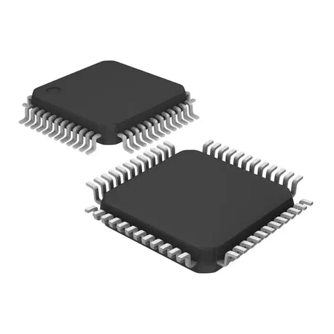
−LQFP64 10x10 mm
−LQFP64 7x7 mm
−LQFP48 7x 7 mm
−LQFP48 6 x 6 mm
−QFN32 4 x 4 mm
List of Models
Table 1. Device summary
Internal Flash
Memory
Model
256 Kbytes
AT32F415RCT7, AT32F415RCT7-7,
AT32F415CCT7, AT32F415CCU7,
AT32F415KCU7-4
128 Kbytes
AT32F415RBT7, AT32F415RBT7-7,
AT32F415CBT7, AT32F415CBU7,
AT32F415KBU7-4
64 Kbytes
AT32F415R8T7, AT32F415R8T7-7,
AT32F415C8T7, AT32F415K8U7-4

AT32F415 Series Reference Manual
2020.06.28 Page 2 Version 1.02
Contents
1System Architecture ............................................................................................41
1.1 System Introduction.........................................................................................41
1.1.1 Bus Architecture .....................................................................................43
1.1.2 ARM Cortex®-M4 Processer .....................................................................43
1.2 Address Map ...................................................................................................44
1.2.1 Register Map ..........................................................................................46
1.2.2 Bit Banding.............................................................................................47
1.2.3 On-chip SRAM ........................................................................................48
1.2.4 On-chip Flash .........................................................................................48
1.3 Boot Configuration...........................................................................................51
1.4 Device Characteristics Information ...................................................................53
1.4.1 Description of Register Abbreviations .......................................................53
1.4.2 Flash Memory Size Register ....................................................................53
1.4.3 Device Electronic Signature .....................................................................53
2Power Control (PWR) ...........................................................................................55
2.1 Introduction.....................................................................................................55
2.2 Main Features .................................................................................................55
2.3 Function Overview ...........................................................................................55
2.3.1 Power Supply..........................................................................................55
2.3.1.1 VDD/VDDA Power Domain...............................................................56
2.3.1.2 Core Power Domain ........................................................................58
2.3.2 Low-power Mode.....................................................................................58
2.3.2.1 Sleep Mode ....................................................................................59
2.3.2.2 Stop Mode......................................................................................60
2.3.2.3 Standby Mode.................................................................................61
2.3.2.4 Debug Mode ...................................................................................62
2.3.3 Auto-wakeup (AWU) ................................................................................62
2.4 PWR Registers................................................................................................63
2.4.1 Power Control Register (PWR_CTRL).......................................................63
2.4.2 Power Control/Status Register (PWR_CTRLSTS) ......................................64
3Reset and Clock Control (RCC)............................................................................65

AT32F415 Series Reference Manual
2020.06.28 Page 3 Version 1.02
3.1 Reset..............................................................................................................65
3.1.1 System Reset .........................................................................................65
3.1.2 Power Reset ...........................................................................................65
3.1.3 Backup Domain Reset .............................................................................66
3.2 Clocks ............................................................................................................66
3.2.1 HSE Clock ..............................................................................................68
3.2.2 HSI Clock ...............................................................................................69
3.2.3 PLL ........................................................................................................69
3.2.4 LSE Clock ..............................................................................................70
3.2.5 LSI Clock................................................................................................70
3.2.6 System Clock (SYSCLK) Selection ...........................................................71
3.2.7 Clock Failure Detection (CFD) .................................................................71
3.2.8 ERTC Clock............................................................................................71
3.2.9 Watchdog Clock ......................................................................................71
3.2.10 Clock-out Capability ................................................................................72
3.3 RCC Registers Description...............................................................................72
3.3.1 Clock Control Register (RCC_CTRL) ........................................................74
3.3.2 Clock Configuration Register (RCC_CFG) .................................................76
3.3.3 Clock Interrupt Register (RCC_CLKINT) ...................................................78
3.3.4 APB2 Peripheral Reset Register (RCC_APB2RST) ....................................80
3.3.5 APB1 Peripheral Reset Register (RCC_APB1RST) ....................................81
3.3.6 AHB Peripheral Clock Enable Register (RCC_AHBEN)...............................84
3.3.7 APB2 Peripheral Clock Enable Register (RCC_APB2EN) ...........................84
3.3.8 APB1 Peripheral Clock Enable Register (RCC_APB1EN) ...........................86
3.3.9 Backup Domain Control Register (RCC_BDC) ...........................................88
3.3.10 Control/Status register (RCC_CTRLSTS) ..................................................89
3.3.11 AHB Peripheral Reset Register (RCC_AHBRST) .......................................90
3.3.12 PLL Configuration Register (RCC_PLL) ....................................................90
3.3.13 Additional Register (RCC_MISC)..............................................................91
3.3.14 OTG_FS Extension Control Register (RCC_OTG_EXTCTRL) .....................92
3.3.15 Additional Register (RCC_MISC2) ............................................................93
4Embedded Flash Controller (EFC)........................................................................94

AT32F415 Series Reference Manual
2020.06.28 Page 4 Version 1.02
4.1 EFC Introduction .............................................................................................94
4.2 Main Features .................................................................................................94
4.2.1 Flash Memory Architecture ......................................................................94
4.3 Function Overview ...........................................................................................97
4.3.1 Read Operation.......................................................................................97
4.3.1.1 Instruction Fetch.............................................................................97
4.3.1.2 D-Code Interface ............................................................................98
4.3.1.3 Flash Access Controller...................................................................98
4.3.2 Flash Program/Erase Controller (FPEC) ...................................................98
4.3.2.1 Key Value.......................................................................................98
4.3.2.2 Unlock the Flash Memory ................................................................98
4.3.2.3 Main Flash Programming .................................................................98
4.3.2.4 Flash Erase ....................................................................................99
4.3.2.5 Option Byte Programming ..............................................................101
4.3.3 Protection.............................................................................................102
4.3.3.1 Write Protection............................................................................102
4.3.3.2 Read Protection ............................................................................102
4.3.3.3 Option Byte Block Write Protection.................................................104
4.3.4 Option Byte Description.........................................................................104
4.3.5 Special Functions..................................................................................105
4.3.5.1 Security Library Setting ......................................................................105
4.3.5.2 System Memory for Main Memory Extension Purpose ...........................106
4.3.5.3 CRC Calibration .................................................................................107
4.4 EFC Registers...............................................................................................108
4.4.1 Flash Access Control Register (FLASH_ACR) .........................................109
4.4.2 FPEC Key Register (FLASH_FCKEY) .....................................................110
4.4.3 Flash OPTKEY Register (FLASH_OPTKEYR) ..........................................110
4.4.4 Flash Status Register (FLASH_STS) ......................................................111
4.4.5 Flash Control Register (FLASH_CTRL) ...................................................112
4.4.6 Flash Address Register (FLASH_ADDR) .................................................113
4.4.7 Option Byte Register (FLASH_UOB) .......................................................113
4.4.8 Write Protection Register (FLASH_WRPRT)............................................114

AT32F415 Series Reference Manual
2020.06.28 Page 5 Version 1.02
4.4.9 Flash sLib Status Register 0 (FLASH_CDR0) ..........................................114
4.4.10 Flash sLib Status Register 1 (FLASH_CDR1) ..........................................115
4.4.11 Flash sLib Password Register (FSLIB_PSW)...........................................117
4.4.12 Flash sLib Password Setting Status Register (FLASH_PSW_STS) ............117
4.4.13 Flash CRC Verify Start Position (FLASH_CRC_AR) ................................. 118
4.4.14 Flash CRC Verify Control Register (FLASH_CRC_CTRL) .........................118
4.4.15 Flash CRC Verify Result Register (FLASH_CRC_OUTR)..........................119
4.4.16 Flash sLib Password Setting Register (FLASH_SET_PSW) ......................119
4.4.17 Flash sLib Rang Setting Register (FLASH_SET_RANGE).........................119
4.4.18 Main memory Extension Area sLib Setting Register (SYS_MEM_SLIB_SET).
............................................................................................................120
4.4.19 Flash memory Extension Area Mode Register (SYS_MEM_BOOT_DIS_SET).
............................................................................................................120
4.4.20 Flash sLib key Register (FSLIB_KEYR) ..................................................121
5CRC Calculation Unit (CRC) ...............................................................................122
5.1 CRC Introduction...........................................................................................122
5.2 CRC Main Features .......................................................................................122
5.3 CRC Function Overview .................................................................................123
5.4 CRC Registers ..............................................................................................124
5.4.1 Data Register (CRC_DR) .......................................................................124
5.4.2 Independent Data Register (CRC_IDR)...................................................124
5.4.3 Control Register (CRC_CTRL) ...............................................................125
5.4.4 CRC Initial Value (CRC_INIT) ................................................................126
6General-purpose and Alternate-function I/Os (GPIOs and AFIOs) ......................127
6.1 Introduction...................................................................................................127
6.2 Main Features ...............................................................................................127
6.3 Function Overview .........................................................................................127
6.3.1 GPIO Pin Configuration .........................................................................127
6.3.2 External Interrupt/Wakeup Lines ............................................................129
6.3.3 Input Configuration................................................................................129
6.3.4 Analog Input Configuration ....................................................................130
6.3.5 Output Configuration .............................................................................131
6.3.6 GPIO Locking Mechanism......................................................................132

AT32F415 Series Reference Manual
2020.06.28 Page 6 Version 1.02
6.3.7 Alternate Function (AF) .........................................................................132
6.4 IO Mapping Function Configuration ................................................................. 136
6.4.1 OSC32_IN/OSC32_OUT as GPIO Interface PC14/PC15 ...........................136
6.4.2 OSC_IN/OSC_OUT Pin as GPIO Interface PD0/PD1 ................................136
6.4.3 CAN Alternate Function Remapping........................................................136
6.4.4 JTAG/SWD Alternate Function Remapping ..............................................136
6.4.5 ADC Alternate Function Remapping........................................................137
6.4.6 Timer Alternate Function Remapping ......................................................138
6.4.7 USART Alternate Function Remapping ...................................................139
6.4.8 I2C Alternate Function Remapping..........................................................140
6.4.9 SPI1/I2S1 Alternate Function Remapping ...............................................140
6.4.10 SDIO Alternate Function Remapping ......................................................140
6.4.11 COMP Alternate Function Remapping .....................................................141
6.5 GPIO and AFIO Registers ..............................................................................141
6.5.1 Port Configuration Register Low (GPIOx_CTRLL) (x = A…E) .............................143
6.5.2 Port Configuration Register High (GPIOx_CTRLH) (A...E) ........................144
6.5.3 Port Input Data Register (GPIOx_IPTDT) (x = A...E) ................................145
6.5.4 Port Output Data Register (GPIOx_OPTDT) (x = A...E) ............................145
6.5.5 Port Bit Set/Reset Register (GPIOx_BSRE) (x = A...E) ............................145
6.5.6 Port Bit Reset Register (IOx_BRE) (x = A...E) .........................................146
6.5.7 Port Configuration Lock Register (GPIOx_LOCK) (x = A...E) ....................146
6.5.8 Alternate Event Control Register (AFIO_EVCTRL)...................................147
6.5.9 AF Remap and Debug I/O Configuration Register (AFIO_MAP).................147
6.5.10 Alternate External Interrupt Configuration Register 1 (AFIO_EXTIC1) .......149
6.5.11 Alternate External Interrupt Configuration Register 2 (AFIO_EXTIC2) .......150
6.5.12 Alternate External Interrupt Configuration Register 3 (AFIO_EXTIC3) .......151
6.5.13 Alternate External Interrupt Configuration Register 4 (AFIO_EXTIC4) .......151
6.5.14 AF Remap and Debug I/O Configuration Register 2 (AFIO_MAP2) ............151
6.5.15 AF Remap and Debug I/O Configuration Register 3 (AFIO_MAP3) ............152
6.5.16 AF Remap and Debug I/O Configuration Register 4 (AFIO_MAP4) ............153
6.5.17 AF Remap and Debug I/O Configuration Register 5 (AFIO_MAP5) ............154
6.5.18 AF Remap and Debug I/O Configuration Register 6 (AFIO_MAP6) ............155

AT32F415 Series Reference Manual
2020.06.28 Page 7 Version 1.02
6.5.19 AF Remap and Debug I/O Configuration Register 7 (AFIO_MAP7) ............155
6.5.20 AF Remap and Debug I/O Configuration Register 8 (AFIO_MAP8) ............157
7Interrupts and Events ........................................................................................158
7.1 Nested Vectored Interrupt Controller...............................................................158
7.1.1 System Tick (SysTick) Calibration Value Register ...................................158
7.1.2 Interrupt and Exception Vectors .............................................................158
7.2 External Interrupt/Event Controller (EXTI) .......................................................161
7.2.1 Main Features.......................................................................................161
7.2.2 Block Diagram ......................................................................................161
7.2.3 Wakeup Event Management...................................................................161
7.2.4 Function Overview ................................................................................162
7.2.5 External Interrupt/Event Line Mapping ....................................................162
7.3 EXTI Registers Description ............................................................................164
7.3.1 Interrupt Mask Register (EXTI_INTEN) ...................................................164
7.3.2 Event Mask Register (EXTI_EVTEN) ......................................................165
7.3.3 Rising Edge Trigger Selection Register (EXTI_RTRSEL)..........................165
7.3.4 Falling Edge Trigger Selection Register (EXTI_FTRSEL) .........................165
7.3.5 Software Interrupt Event Register (EXTI_SWIE) ......................................166
7.3.6 Pending Register (EXTI_PND) ...............................................................166
8DMA Controller (DMA)........................................................................................167
8.1 DMA Introduction...........................................................................................167
8.2 DMA Main Features .......................................................................................167
8.3 Function Overview .........................................................................................168
8.3.1 DMA Transaction ..................................................................................168
8.3.2 Arbiter..................................................................................................169
8.3.3 DMA Channels ......................................................................................169
8.3.4 Programmable Data Transfer Width, Alignment, and Endian ...............................170
8.3.5 Error Management ................................................................................171
8.3.6 Interrupts..............................................................................................172
8.3.7 Fixed DMA Request Mapping ................................................................. 172
8.3.8 Flexible DMA Request Mapping..............................................................175
8.4 DMA Registers ..............................................................................................177

AT32F415 Series Reference Manual
2020.06.28 Page 8 Version 1.02
8.4.1 DMA Interrupt Status Register (DMA_ISTS) ............................................179
8.4.2 DMA Interrupt Flag Clear Register (DMA_ICLR) ......................................180
8.4.3 DMA Channel x Configuration Register (DMA_CHCTRLx) (x = 1 … 7).......180
8.4.4 DMA Channel x Number of Data Register (DMA_TCNTx) (x = 1 … 7)........182
8.4.5 DMA Channel x Peripheral Address Register (DMA_CPBAx) (x = 1 … 7)...182
8.4.6 DMA Channel x Memory Address Register (DMA_CMBAx) (x = 1 … 7)......183
8.4.7 DMA Source Register0 (DMA_SRC_SEL0) ..............................................184
8.4.8 DMA Source Register1 (DMA_SRC_SEL1) ..............................................184
9Timer .................................................................................................................185
9.1 General-purpose Basic Timer (TMR2 to TMR5)................................................185
9.1.1 TMRx Introduction.................................................................................185
9.1.2 TMRx Main Features .............................................................................185
9.1.3 TMRx Function Overview .......................................................................186
9.1.3.1 Time-base Unit .............................................................................186
9.1.3.2 Counting Mode .............................................................................188
9.1.3.3 Clock Selection.............................................................................195
9.1.3.4 Capture/Compare Channel.............................................................197
9.1.3.5 Input Capture Mode ......................................................................199
9.1.3.6 PWM Input Mode...........................................................................200
9.1.3.7 Forced Output Mode......................................................................201
9.1.3.8 Output Compare Mode ..................................................................201
9.1.3.9 PWM Mode...................................................................................203
9.1.3.10 One-pulse Mode ...........................................................................205
9.1.3.11 Clearing OCxREF Signal on an External Event................................206
9.1.3.12 Encoder Interface Mode ................................................................207
9.1.3.13 Timer Input XOR Function .............................................................208
9.1.3.14 Timer and External Trigger Synchronization....................................208
9.1.3.15 Timer Synchronization...................................................................211
9.1.3.16 Debug Mode .................................................................................215
9.1.4 TMRx Registers ....................................................................................216
9.1.4.1 Control Register 1 (TMRx_CTRL1) .................................................217
9.1.4.2 Control Register 2 (TMRx_CTRL2) .................................................219

AT32F415 Series Reference Manual
2020.06.28 Page 9 Version 1.02
9.1.4.3 Slave Mode Control Register (TMRx_SMC).....................................219
9.1.4.4 DMA/Interrupt Enable Register (TMRx_DIE)....................................221
9.1.4.5 Status Register (TMRx_STS) .........................................................222
9.1.4.6 Event Generation Register (TMRx_EVEG) ......................................223
9.1.4.7 Capture/Compare Mode Register 1 (TMRx_CCM1) ..........................224
9.1.4.8 Capture/Compare Mode Register 2 (TMRx_CCM2) ..........................226
9.1.4.9 Capture/Compare Enable Register (TMRx_CCE) .............................228
9.1.4.10 Counter (TMRx_CNT)....................................................................229
9.1.4.11 Prescaler (TMRx_DIV)...................................................................229
9.1.4.12 Auto-reload Register (TMRx_AR) ...................................................230
9.1.4.13 Capture/Compare Register 1 (TMRx_CC1)......................................230
9.1.4.14 Capture/Compare Register 2 (TMRx_CC2)......................................231
9.1.4.15 Capture/Compare Register 3 (TMRx_CC3)......................................231
9.1.4.16 Capture/Compare Register 4 (TMRx_CC4)......................................232
9.1.4.17 DMA Control Register (TMRx_DMAC).............................................232
9.1.4.18 DMA Address in Burst Mode (TMRx_DMABA) ................................. 233
9.2 General-purpose Timer (TMR9 to TMR11) .......................................................233
9.2.1 TMRx Introduction.................................................................................233
9.2.2 TMRx Main Function..............................................................................233
9.2.2.1 TMR9 Main Function .....................................................................233
9.2.2.2 TMR10 and TMR11 Main Function..................................................234
9.2.3 TMRx Function Overview .......................................................................236
9.2.3.1 Time-base Unit .............................................................................236
9.2.3.2 Counter Mode...............................................................................237
9.2.3.3 Clock Selection.............................................................................239
9.2.3.4 Capture/Compare Channel.............................................................241
9.2.3.5 Input Capture Mode ......................................................................242
9.2.3.6 PWM Input Mode (Only TMR9).......................................................243
9.2.3.7 Forced Output Mode......................................................................244
9.2.3.8 Output Compare Mode ..................................................................244
9.2.3.9 PWM Mode...................................................................................245
9.2.3.10 One-pulse Mode ...........................................................................246

AT32F415 Series Reference Manual
2020.06.28 Page 10 Version 1.02
9.2.3.11 Timer and External Trigger Synchronization (TMR9 Only) ................247
9.2.3.12 Timer Synchronization (TMR9 Only) ...............................................249
9.2.3.13 Debug Mode.................................................................................249
9.2.4 TMR9 Register Description ....................................................................249
9.2.4.1 Control Register 1 (TMRx_CTRL1) .................................................251
9.2.4.2 Slave Mode Control Register (TMRx_SMC).....................................252
9.2.4.3 DMA/Interrupt Enable Register (TMRx_DIE)....................................253
9.2.4.4 Status Register (TMRx_STS) .........................................................254
9.2.4.5 Event Generation Register (TMRx_EVEG) ......................................255
9.2.4.6 Capture/Compare Mode Register 1 (TMRx_CCM1) ..........................256
9.2.4.7 Capture/Compare Enable Register (TMRx_CCE) .............................259
9.2.4.8 Counter (TMRx_CNT)....................................................................260
9.2.4.9 Prescaler (TMRx_DIV)...................................................................260
9.2.4.10 Auto-reload Register (TMRx_AR) ...................................................260
9.2.4.11 Capture/Compare Register 1 (TMRx_CC1)......................................261
9.2.4.12 Capture/Compare Register 2 (TMRx_CC2)......................................261
9.2.5 TMR10 and TMR11 Registers Description ...............................................261
9.2.5.1 Control Register 1 (TMRx_CTRL1) .................................................262
9.2.5.2 DMA/Interrupt Enable Register (TMRx_DIE)....................................263
9.2.5.3 Status Register (TMRx_STS) .........................................................263
9.2.5.4 Event Generation Register (TMRx_EVEG) ......................................265
9.2.5.5 Capture/Compare Mode Register 1 (TMRx_CCM1) ..........................265
9.2.5.6 Capture/Compare Enable Register (TMRx_CCE) .............................267
9.2.5.7 Counter (TMRx_CNT)....................................................................268
9.2.5.8 Prescaler (TMRx_DIV)...................................................................268
9.2.5.9 Auto-reload Register (TMRx_AR) ...................................................268
9.2.5.10 Capture/Compare Register 1 (TMRx_CC1)......................................269
9.3 Advanced-control Timer (TMR1) .....................................................................270
9.3.1 TMR1 Introduction.................................................................................270
9.3.2 TMR1 Main Features .............................................................................270
9.3.3 TMR1 Function Overview.......................................................................271
9.3.3.1 Time-base Unit .............................................................................271

AT32F415 Series Reference Manual
2020.06.28 Page 11 Version 1.02
9.3.3.2 Counter Mode...............................................................................273
9.3.3.3 Repetition Counter ........................................................................281
9.3.3.4 Clock Selection.............................................................................282
9.3.3.5 Capture/Compare Channel.............................................................284
9.3.3.6 Input Capture Mode ......................................................................286
9.3.3.7 PWM Input Mode...........................................................................287
9.3.3.8 Forced Output Mode......................................................................288
9.3.3.9 Output Compare Mode ..................................................................289
9.3.3.10 PWM Mode...................................................................................290
9.3.3.11 Complementary Output and Dead-time Insertion..............................292
9.3.3.12 Using the Break Function ..............................................................293
9.3.3.13 Clearing OCxREF Signal on an External Event................................295
9.3.3.14 6-step PWM Output Generation......................................................296
9.3.3.15 One-pulse Mode ...........................................................................297
9.3.3.16 Encoder Interface Mode ................................................................299
9.3.3.17 Timer Input XOR Function .............................................................300
9.3.3.18 Interfacing with Hall Sensors .........................................................301
9.3.3.19 TMRx Timer and External Trigger Synchronization ..........................302
9.3.3.20 Timer Synchronization...................................................................305
9.3.3.21 Debug Mode .................................................................................305
9.3.4 TMR1 Register Description ....................................................................306
9.3.4.1 TMR1 Control Register 1 (TMRx_CTRL1) .......................................307
9.3.4.2 TMR1 Control Register 2 (TMRx_CTRL2) .......................................309
9.3.4.3 TMR1 Slave Mode Control Register (TMRx_SMC) ...........................310
9.3.4.4 TMR1 DMA/Interrupt Enable Register (TMRx_DIE) ..........................311
9.3.4.5 TMR1 Status Register (TMRx_STS) ...............................................312
9.3.4.6 TMR1 Event Generation Register (TMRx_EVEG).............................315
9.3.4.7 TMR1 Capture/Compare Mode Register 1 (TMRx_CCM1) ................315
9.3.4.8 TMR1 Capture/Compare Mode Register 2 (TMRx_CCM2) ................318
9.3.4.9 TMR1 Capture/Compare Enable Register (TMRx_CCE) ...................319
9.3.4.10 TMR1 Counter (TMRx_CNT) ..........................................................322
9.3.4.11 TMR1 Prescaler (TMRx_DIV) .........................................................322

AT32F415 Series Reference Manual
2020.06.28 Page 12 Version 1.02
9.3.4.12 TMR1 Auto-reload Register (TMRx_AR)..........................................322
9.3.4.13 TMR1 Repetition Counter Register (TMRx_RC) ...............................323
9.3.4.14 TMR1 Capture/Compare Register 1 (TMRx_CC1) ............................323
9.3.4.15 TMR1 Capture/Compare Register 2 (TMRx_CC2) ............................323
9.3.4.16 TMR1 Capture/Compare Register 3 (TMRx_CC3) ............................324
9.3.4.17 TMR1 Capture/Compare Register 4 (TMRx_CC4) ............................324
9.3.4.18 TMR1 Break and Dead-time Register (TMRx_BRKDT) .....................325
9.3.4.19 TMR1 DMA Control Register (TMRx_DMAC) ...................................326
9.3.4.20 TMR1 DMA Address in Burst Mode (TMRx_DMABA) ........................327
10 Watchdog ..........................................................................................................328
10.1 Window Watchdog (WWDG) ...........................................................................328
10.1.1 WWDG Introduction...............................................................................328
10.1.2 WWDG Main Features ...........................................................................328
10.1.3 WWDG Function Overview .....................................................................328
10.1.4 How to Program Watchdog Timeout........................................................330
10.1.5 Debug Mode .........................................................................................330
10.1.6 Register Description..............................................................................331
10.1.6.1 Control Register (WWDG_CTRL)....................................................331
10.1.6.2 Configuration Register (WWDG_CFG) ............................................331
10.1.6.3 Status Register (WWDG_STS) .......................................................332
10.2 Independent Watchdog (IWDG) ......................................................................333
10.2.1 Introduction ..........................................................................................333
10.2.2 IWDG Main Features .............................................................................333
10.2.3 IWDG Function Overview .......................................................................333
10.2.3.1 Hardware Watchdog ......................................................................333
10.2.3.2 Register Access Protection............................................................333
10.2.3.3 Debug Mode .................................................................................333
10.2.4 IWDG Register Description ....................................................................334
10.2.4.1 Key Register (IWDG_KEY).............................................................335
10.2.4.2 Prescaler Register (IWDG_PR) ......................................................335
10.2.4.3 Reload Register (IWDG_RLD)........................................................336
10.2.4.4 Status Register (IWDG_STS) .........................................................337

AT32F415 Series Reference Manual
2020.06.28 Page 13 Version 1.02
11 Real-time Clock (ERTC) .....................................................................................338
11.1 Introduction...................................................................................................338
11.2 ERTC Main Features .....................................................................................338
11.3 ERTC Function Overview ...............................................................................339
11.3.1 Clock and Prescaler ..............................................................................339
11.3.2 Real-time Clock and Calendar................................................................340
11.3.3 Programmable Clock .............................................................................340
11.3.4 Periodic Auto-wakeup............................................................................341
11.3.5 ERTC Initialization and Configuration .....................................................341
11.3.6 Read the Calendar ................................................................................343
11.3.7 Reset ERTC..........................................................................................344
11.3.8 ERTC Synchronization...........................................................................344
11.3.9 ERTC Reference Clock Detection...........................................................344
11.3.10 ERTC Coarse Digital Calibration ............................................................345
11.3.11 ERTC Fine Digital Calibration ................................................................346
11.3.12 Time Stamp Function.............................................................................347
11.3.13 Tamper Detection..................................................................................348
11.3.14 Calibration Clock Output........................................................................349
11.3.15 Alarm Clock Output ...............................................................................349
11.4 ERTC and Low-power Mode ...........................................................................349
11.5 ERTC Interrupt..............................................................................................350
11.6 ERTC Register ..............................................................................................351
11.6.1 ERTC Time Register (ERTC_TIME) ........................................................351
11.6.2 ERTC Date Register (ERTC_DATE)........................................................352
11.6.3 ERTC Control Register (ERTC_CTRL) ....................................................352
11.6.4 ERTC Initialization and Status Register (ERTC_STS) ..............................354
11.6.5 ERTC Prescaler Register (ERTC_PSC)...................................................355
11.6.6 ERTC Wakeup Timer Register (ERTC_WATR).........................................356
11.6.7 ERTC Calibration Register (ERTC_CAL) .................................................356
11.6.8 ERTC Alarm Clock A Register (ERTC_ALA) ............................................357
11.6.9 ERTC Alarm Clock B Register (ERTC_ALB) ............................................358
11.6.10 ERTC Write Protect Register (EERTC_WPR) ..........................................358

AT32F415 Series Reference Manual
2020.06.28 Page 14 Version 1.02
11.6.11 ERTC Sub-second Register (ERTC_SBSR) .............................................359
11.6.12 ERTC Shift Control Register (ERTC_SFCTR) ..........................................359
11.6.13 ERTC Time Stamp Time Register (ERTC_TSTM).....................................360
11.6.14 ERTC Time Stamp Date Register (ERTC_TSDT) .....................................360
11.6.15 ERTC Time Stamp Sub-second Register (ERTC_TSSBS).........................361
11.6.16 ERTC Calibration Register (ERTC_CCR) ................................................361
11.6.17 ERTC Tamper and Alternate Function Configuration Register (ERTC_TPAF)362
11.6.18 ERTC Alarm Clock A Sub-second Register (ERTC_ALASBS) ...................363
11.6.19 ERTC Alarm Clock B Sub-second Register (ERTC_ALBSBS) ...................363
11.6.20 ERTC Backup Register (ERTC_BKPxDT) ................................................364
12 Analog-to-Digital Converter (ADC) .....................................................................365
12.1 ADC Introduction ...........................................................................................365
12.2 ADC Main Features .......................................................................................365
12.3 ADC Function Overview .................................................................................365
12.3.1 ADC Switch ..........................................................................................367
12.3.2 ADC Clock............................................................................................367
12.3.3 Channel Selection .................................................................................367
12.3.4 Single Conversion Mode ........................................................................367
12.3.5 Continuous Conversion Mode................................................................. 368
12.3.6 Timing Diagram.....................................................................................368
12.3.7 Analog Watchdog ..................................................................................368
12.3.8 Scan Mode ...........................................................................................369
12.3.9 Injected Channel Management...............................................................369
12.3.10 Discontinuous Mode ..............................................................................370
12.3.11 Calibration............................................................................................371
12.3.12 Data Alignment .....................................................................................372
12.3.13 Programmable Channel Sample Time .....................................................372
12.3.14 Conversion on External Trigger ..............................................................372
12.3.15 DMA Request........................................................................................374
12.3.16 Temperature Sensor..............................................................................374
12.3.17 ADC Interrupts......................................................................................375
12.4 ADC Registers ..............................................................................................375

AT32F415 Series Reference Manual
2020.06.28 Page 15 Version 1.02
12.4.1 ADC Status Register (ADC_STS) ...........................................................377
12.4.2 ADC Control Register 1 (ADC_CTRL1) ...................................................377
12.4.3 ADC Control Register 2 (ADC_CTRL2) ...................................................380
12.4.4 ADC Sample Time Register 1 (ADC_SMPT1) ..........................................383
12.4.5 ADC Sample Time Register 2 (ADC_SMPT2) ..........................................383
12.4.6 ADC Injected Channel Data Offset Register x (ADC_JOFSx) (x = 1…4) ....384
12.4.7 ADC Watchdog High Threshold Register (ADC_WHTR)............................384
12.4.8 ADC Watchdog Low Threshold Register (ADC_WLTR) .............................385
12.4.9 ADC Regular Sequence Register 1 (ADC_RSQ1) ....................................385
12.4.10 ADC Regular Sequence Register 2 (ADC_RSQ2) ....................................385
12.4.11 ADC Regular Sequence Register 3 (ADC_RSQ3) ....................................386
12.4.12 ADC Injected Sequence Register (ADC_JSQ) .........................................387
12.4.13 ADC Injected Data Register x (ADC_JDORx) (x = 1…4) ...........................387
12.4.14 ADC Regular Data Register (ADC_RDOR) ..............................................388
13 I2C Interface.......................................................................................................389
13.1 I2C Introduction .............................................................................................389
13.2 I2C Main Features..........................................................................................389
13.3 I2C Function Overview ...................................................................................390
13.3.1 Mode Selection .....................................................................................390
13.3.2 I2C Slave Mode .....................................................................................391
13.3.3 I2C Master Mode ...................................................................................393
13.3.4 Error Condition .....................................................................................398
13.3.5 SDA/SCL Line Control ...........................................................................399
13.3.6 SMBus ................................................................................................. 399
13.3.7 DMA Request........................................................................................401
13.3.8 Packet Error Checking (PEC) ................................................................. 402
13.3.9 I2C Interrupt Request.............................................................................403
13.3.10 I2C Debug Mode....................................................................................404
13.4 I2C Registers................................................................................................. 404
13.4.1 Control Register 1 (I2C_CTRL1) .............................................................405
13.4.2 Control Register 2 (I2C_CTRL2) .............................................................407
13.4.3 Own Address Register 1 (I2C_OADDR1) .................................................408

AT32F415 Series Reference Manual
2020.06.28 Page 16 Version 1.02
13.4.4 Own Address Register 2 (I2C_OADDR2) .................................................409
13.4.5 Data Register (I2C_DT)..........................................................................409
13.4.6 Status Register 1 (I2C_STS1)................................................................. 409
13.4.7 Status Register 2 (I2C_STS2)................................................................. 412
13.4.8 Clock Control Register (I2C_CLKCTRL) ..................................................413
13.4.9 TMRISE Register (I2C_TMRISE).............................................................414
14 Universal Synchronous/Asynchronous Receiver/Transmitter (USART) ..............415
14.1 USART Introduction.......................................................................................415
14.2 USART Main Features ...................................................................................415
14.3 USART Function Overview .............................................................................416
14.3.1 USART Feature Description ...................................................................417
14.3.2 Transmitter ...........................................................................................418
14.3.2.1 Character Transmission................................................................. 418
14.3.2.2 Configurable Stop Bit ....................................................................419
14.3.2.3 Single Byte Communication ...........................................................420
14.3.2.4 Break Frame.................................................................................420
14.3.2.5 Idle Character...............................................................................421
14.3.3 Receiver...............................................................................................421
14.3.3.1 Start Bit Detection.........................................................................421
14.3.3.2 Character Reception .....................................................................422
14.3.3.3 Break Frame.................................................................................422
14.3.3.4 Idle Frame....................................................................................422
14.3.3.5 Overrun Error ...............................................................................422
14.3.3.6 Framing Error ...............................................................................424
14.3.3.7 Configurable Stop Bits during Reception.........................................424
14.3.4 Fractional Baud Rate Generation ...........................................................424
14.3.4.1 How to Derive USARTDIV from USART_ BAUDR Register Values ....425
14.3.5 USART Receiver’s Tolerance to Clock Deviation .....................................426
14.3.6 Multiprocessor Communication...............................................................426
14.3.6.1 Idle Line Detection (WUMODE = 0) ................................................427
14.3.6.2 Address Mark Detection (WUMODE = 1).........................................427
14.3.7 Parity Control .......................................................................................427

AT32F415 Series Reference Manual
2020.06.28 Page 17 Version 1.02
14.3.8 LIN (Local Interconnection Network) Mode..............................................428
14.3.8.1 LIN Transmission ..........................................................................428
14.3.8.2 LIN Reception...............................................................................428
14.3.9 USART Synchronous Mode ....................................................................430
14.3.10 Single-wire Half-duplex Communication ..................................................432
14.3.11 Smartcard.............................................................................................433
14.3.12 IrDA SIR ENDEC Block..........................................................................435
14.3.13 Continuous Communication Using DMA ..................................................436
14.3.13.1 Transmission Using DMA...............................................................436
14.3.13.2 Reception Using DMA ...................................................................437
14.3.13.3 Error Flag and Interrupt Generation in Multi-buffer Communication...438
14.3.14 Hardware Flow Control ..........................................................................438
14.3.14.1 RTS Flow Control..........................................................................438
14.3.14.2 CTS Flow Control..........................................................................439
14.4 USART Interrupt Request...............................................................................439
14.5 USART Mode Configuration............................................................................440
14.6 USART Registers ..........................................................................................440
14.6.1 USART Register Map ............................................................................440
14.6.2 Status Register (USART_STS) ...............................................................441
14.6.3 Data Register (USART_DT) ...................................................................443
14.6.4 Baud Rate Register (USART_BAUDR) ....................................................443
14.6.5 Control Register 1 (USART_CTRL1) .......................................................444
14.6.6 Control Register 2 (USART_CTRL2) .......................................................445
14.6.7 Control Register 3 (USART_CTRL3) .......................................................447
14.6.8 Guard Time and Prescaler Register (GTP) ..............................................448
15 Serial Peripheral Interface (SPI) ........................................................................450
15.1 SPI Introduction ............................................................................................450
15.2 Main Features ...............................................................................................450
15.2.1 SPI Main Features ................................................................................450
15.2.2 I2S Function Overview ...........................................................................450
15.3 Function Overview .........................................................................................451
15.3.1 SPI Function Overview ..........................................................................451

AT32F415 Series Reference Manual
2020.06.28 Page 18 Version 1.02
15.3.1.1 Introduction ..................................................................................451
15.3.1.2 Configure SPI in Slave Mode .........................................................454
15.3.1.3 Configure SPI in Master Mode .......................................................455
15.3.1.4 Configure SPI for Half-duplex Communication................................. 456
15.3.1.5 Data Transmission and Reception ..................................................456
15.3.1.6 CRC Calculation ...........................................................................462
15.3.1.7 Status Flag...................................................................................463
15.3.1.8 Disabling SPI................................................................................464
15.3.1.9 SPI Communication Using DMA .....................................................464
15.3.1.10 Error Flag.....................................................................................466
15.3.1.11 SPI Interrupt.................................................................................467
15.3.2 I2S Function Overview ...........................................................................467
15.3.2.1 I2S Function Overview ...................................................................467
15.3.2.2 Supported Audio Protocol ..............................................................469
15.3.2.3 Clock Generator............................................................................475
15.3.2.4 I2S Master Mode ...........................................................................477
15.3.2.5 I2S Slave Mode .............................................................................478
15.3.2.6 Status Flag...................................................................................479
15.3.2.7 Error Flag.....................................................................................480
15.3.2.8 I2S Interrupt..................................................................................481
15.3.2.9 DMA Function ...............................................................................481
15.4 SPI Registers................................................................................................481
15.4.1 SPI Control Register 1 (SPI_CTRL1) (Not Used in I2S Mode) ...................483
15.4.2 SPI Control Register 2 (SPI_CTRL2) ......................................................484
15.4.3 SPI Status Register (SPI_STS) ..............................................................485
15.4.4 SPI Data Register (SPI_DT)...................................................................486
15.4.5 SPICRC Polynomial Register (SPI_CPOLY) (Not Used in I2S Mode) .........486
15.4.6 SPIRxCRC Register (SPI_RCRC) (Not Used in I2S Mode) ........................487
15.4.7 SPITxCRC Register (SPI_TCRC)............................................................487
15.4.8 SPI_I2S Configuration Register (SPI_I2SCTRL) ......................................487
15.4.9 SPI_I2S Prescaler Register (SPI_I2SCLKP) ............................................489
16 CAN Bus Controller ...........................................................................................490

AT32F415 Series Reference Manual
2020.06.28 Page 19 Version 1.02
16.1 Introduction...................................................................................................490
16.2 Main Features ...............................................................................................490
16.3 Function Overview .........................................................................................490
16.3.1 CAN Overall Function Description ..........................................................490
16.3.2 Operating Mode ....................................................................................492
16.3.2.1 Initialization Mode.........................................................................492
16.3.2.2 Normal Mode ................................................................................493
16.3.2.3 Sleep Mode (Low Power)...............................................................493
16.3.3 Test Mode ............................................................................................494
16.3.3.1 Silent Mode ..................................................................................494
16.3.3.2 Loopback Mode ............................................................................494
16.3.3.3 Loopback and Silent Mode.............................................................495
16.3.4 AT32F415 in Debug Mode......................................................................495
16.3.5 Transmission Handling ..........................................................................495
16.3.6 Time-triggered Communication Mode......................................................496
16.3.7 Reception Handling ...............................................................................497
16.3.8 Identifier Filtering..................................................................................498
16.3.9 Message Storage ..................................................................................501
16.3.10 Error Management ................................................................................503
16.3.11 Bit Timing.............................................................................................503
16.3.12 bxCAN Interrupt ....................................................................................506
16.4 CAN Registers ..............................................................................................507
16.4.1 Register Access Protection ....................................................................509
16.4.2 CAN Control and Status Register ...........................................................509
16.4.2.1 CAN Main Control Register (CAN_MCTRL) .....................................509
16.4.2.2 CAN Main Status Register (CAN_MSTS).........................................511
16.4.2.3 CAN Tx Status Register (CAN_TSTS).............................................512
16.4.2.4 CAN Receive FIFO 0 Register (CAN_RF0) ......................................514
16.4.2.5 CAN Receive FIFO 1 Register (CAN_RF1) ......................................514
16.4.2.6 CAN Interrupts Enable Register (CAN_INTEN) ................................515
16.4.2.7 CAN Error Status Register (CAN_ESTS).........................................516
16.4.2.8 CAN Bit Timing Register (CAN_BTMG) ...........................................517

AT32F415 Series Reference Manual
2020.06.28 Page 20 Version 1.02
16.4.3 CAN Mailbox Register ...........................................................................518
16.4.3.1 Tx Mailbox Identifier Register (CAN_TMIx) (x = 0…2) ......................518
16.4.3.2 Mailbox Data Length and Time Stamp Register (CAN_TDTx)
(x = 0…2) ....................................................................................................519
16.4.3.3 Tx Mailbox Data Low Register (CAN_TDLx) (x = 0...2).....................520
16.4.3.4 Tx Mailbox Data High Register (CAN_TDHx) (x = 0…2) ...................520
16.4.3.5 Rx FIFO Mailbox Identifier Register (CAN_RFIx) (x = 0…1) .............521
16.4.3.6 Rx FIFO Mailbox Data Length and Time Stamp Register
(CAN_RDTx) (x = 0…1)..................................................................................521
16.4.3.7 Rx FIFO Mailbox Data High Register (CAN_RDLx) (x = 0…1) ...........522
16.4.3.8 Rx FIFO Mailbox Data High Register (CAN_RDHx) (x = 0…1) ..........522
16.4.4 CAN Filter Register ...............................................................................523
16.4.4.1 CAN Filter Main Control Register (CAN_FM) ...................................523
16.4.4.2 CAN Filter Mode Register (CAN_FM1)............................................524
16.4.4.3 CAN Filter Scale Register (CAN_FS1) ............................................524
16.4.4.4 CAN Filter FIFO Assignment Register (CAN_FFA1) .........................524
16.4.4.5 CAN Filter Activation Register (CAN_FA1) ......................................525
16.4.4.6 CAN Filter Bank i Register x (CAN_FBiRx)
(where i = 0…13; x = 1…2).............................................................................525
17 SDIO Interface ...................................................................................................527
17.1 Introduction...................................................................................................527
17.2 Main Features ...............................................................................................527
17.3 Function Overview .........................................................................................529
17.3.1 SDIO Function Overview........................................................................529
17.3.1.1 SDIO Adapter ...............................................................................530
17.3.1.2 SDIO AHB Interface ......................................................................538
17.3.2 Card Function Overview ........................................................................539
17.3.2.1 Card Identification Mode................................................................539
17.3.2.2 Card Reset ...................................................................................539
17.3.2.3 Operating Voltage Range Validation ...............................................539
17.3.2.4 Card Identification Process............................................................540
17.3.2.5 Block Write...................................................................................541
17.3.2.6 Block Read...................................................................................541
Other manuals for AT32F415 Series
1
This manual suits for next models
14
Table of contents
Other ARTERY Microcontroller manuals

ARTERY
ARTERY AT32F435 Series Guide

ARTERY
ARTERY AT32 Installation and operating instructions

ARTERY
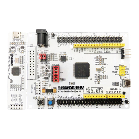
ARTERY AT-START-F403A User manual

ARTERY
ARTERY AT32F421C8T7 User manual

ARTERY
ARTERY AT32F421 Series User manual

ARTERY
ARTERY AT32F421 GPIO User manual

ARTERY
ARTERY AT32F403 Series Specification sheet

ARTERY
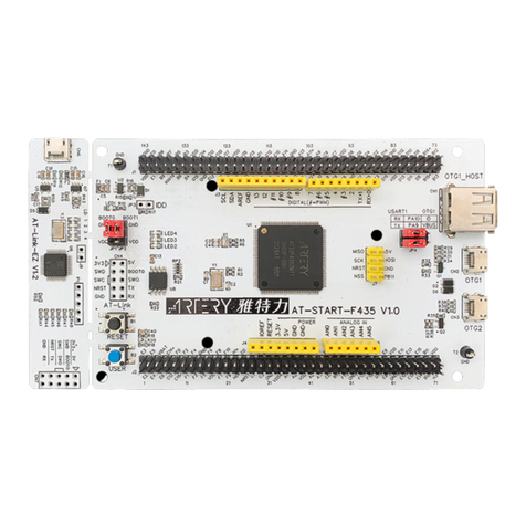
ARTERY AT-START-F435 User manual