ARTERY AT-START-F435 User manual

AT-START-F435 User Manual
2021.11.20 1Rev 1.00
www.arterytek.com
Getting started with AT32F435ZMT7
Introduction
AT-START-F435 is designed to help you explore the high performance of the 32-bit microcontroller
AT32F435 that embeds ARM Cortex®-M4 core with FPU, and expedite application development.
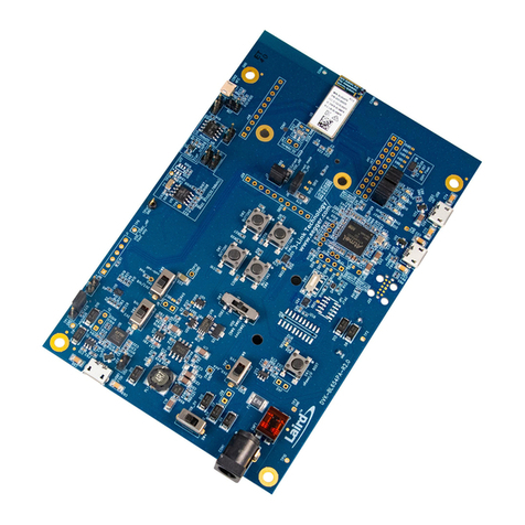
AT-START-F435 is an evaluation board based on AT32F435ZMT7 microcontroller. The device
contains such peripherals as LEDs, buttons, two USB micro-B connectors, type-A connector,
ArduinoTM Uno R3 extension interfaces and 16 MB SPI Flash memory (extended through QSPI1).
This evaluation board embeds AT-Link-EZ for debugging/programming without the need of other
development tools.

AT-START-F435 User Manual
2021.11.20 2Rev 1.00
Contents
1Overview................................................................................................................. 5
1.1 Features ...................................................................................................................5
1.2 Definition of terms .................................................................................................... 5
2Quick start .............................................................................................................. 6
2.1 Get started................................................................................................................6
2.2 AT-START-F435 development toolchains ................................................................. 6
3Hardware and layout ............................................................................................. 7
3.1 Power supply selection............................................................................................. 9
3.2 IDD ........................................................................................................................... 9
3.3 Programming and debugging: embedded AT-Link-EZ .............................................. 9
3.4Boot mode selection............................................................................................... 10
3.5 External clock source .............................................................................................10
3.5.1 HEXT clock source.....................................................................................................10
3.5.2 LEXT clock source .....................................................................................................10
3.6 LEDs .......................................................................................................................11
3.7 Buttons ....................................................................................................................11
3.8 OTGFS configuration...............................................................................................11
3.9 QSPI1 interfacing Flash memory.............................................................................11
3.10 0Ω resistors ............................................................................................................12
3.11 Extension interfaces ............................................................................................... 13
3.11.1 ArduinoTM Uno R3 interface.......................................................................................13
3.11.2 LQFP144 I/O extension interface...............................................................................14
4Schematic ............................................................................................................. 15
5Revision history................................................................................................... 19

AT-START-F435 User Manual
2021.11.20 3Rev 1.00
List of tables
Table 1. Boot mode selection jumper settings...................................................................................10
Table 2. 0Ωresistor settings ...............................................................................................................12
Table 3. ArduinoTM Uno R3 extension interface pin definition...........................................................13
Table 4. Document revision history....................................................................................................19

AT-START-F435 User Manual
2021.11.20 4Rev 1.00
List of figures
Figure 1. Hardware block diagram ......................................................................................................7
Figure 2. Top layer ...............................................................................................................................8
Figure 3. Bottom layer .........................................................................................................................8
Figure 4. Schematic (AT-Link-EZ).....................................................................................................15
Figure 5. Schematic (microcontroller)................................................................................................16
Figure 6. Schematic (power supply and peripherals)........................................................................17
Figure 7. Schematic (extension interfaces).......................................................................................18

AT-START-F435 User Manual
2021.11.20 5Rev 1.00
1 Overview
1.1 Features
AT-START-F435 has the following characteristics:
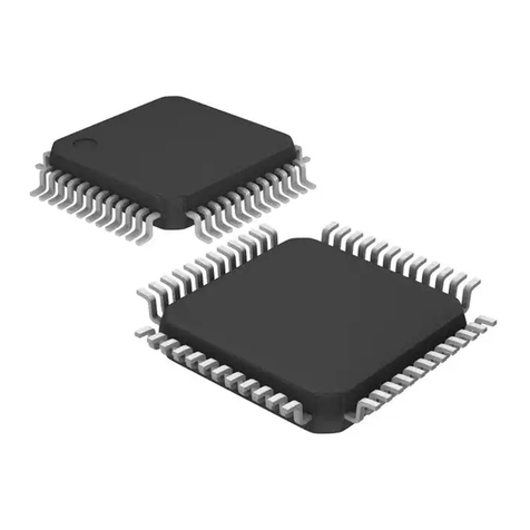
AT-START-F435 has an on-board AT32F435ZMT7 microcontroller that embeds ARM Cortex®-
M4F 32-bit core with FPU, 4032 KB Flash memory and 384 KB SRAM, in LQFP144 packages.
On-board AT-Link interface:
−On-board AT-Link-EZ can be used for programming and debugging (AT-Link-EZ is a
simplified version of AT-Link, without offline mode support)
−If AT-Link-EZ were disassembled from the board by bending it along the joint, this interface
can be connected to an independent AT-Link for programming and debugging.
On-board 20-pin ARM standard JTAG interface (can be connected to JTAG or SWD connector
for programming and debugging)
16 MB SPI (EN25QH128A) is used as extended Flash memory
Various power supply methods:
−USB bus of AT-Link-EZ
−OTG1 or OTG2 bus (VBUS1 or VBUS2) of AT-START-F435
−External 5 V power supply (E5V)
−External 3.3 V power supply
4 x LED indicators:
−LED1 (red) indicates 3.3 V power-on
−3 x USER LEDs, LED2 (red),LED3 (yellow) and LED4 (green), indicate operation status
User button and Reset button
8 MHz HEXT crystal
32.768 kHz LEXT crystal
On-board USB type-A and micro-B connectors in order to demonstrate OTG1 function
OTG2 has micro-B connector (If the user wants to use OTG2 master mode, an adapter cable
is required)
Rich extension interfaces are available for quick prototyping
−ArduinoTM Uno R3 extension interface
−LQFP144 I/O extension interface
1.2 Definition of terms
Jumper JPx ON
Jumper is installed.
Jumper JPx OFF
Jumped is not installed.
Resistor Rx ON / network resistor PRx ON
Short by solder, 0Ω resistor or network resistor.
Resistor Rx OFF / network resistor PRx OFF
Open.

AT-START-F435 User Manual
2021.11.20 6Rev 1.00
2 Quick start
2.1 Get started
Configure the AT-START-F435 board in the following sequence:
1. Check the Jumper’s position on board:
JP1 is connected to GND or OFF (BOOT0 = 0, and BOOT0 has an pull-down resistor in the
AT32F435ZMT7);
JP2 is connected to GND (BOOT1=0)
JP4 is connected to USART1
2. Connect AT_Link_EZ to PC via a USB cable (Type A to micro-B), and supply power to the
evaluation board via a USB connector CN6. LED1 (red) is always on, and three other LEDs
(LED2 to LED4) start to blink in turn.
3. After pressing the user button (B2), the blinking frequency of three LEDs are changed.
2.2 AT-START-F435 development toolchains
ARM®Keil®: MDK-ARM™
IAR™: EWARM

AT-START-F435 User Manual
2021.11.20 7Rev 1.00
3 Hardware and layout
AT-START-F435 board is designed around an AT32F435ZMT7 microcontroller in LQFP144
package.
Figure 1 shows the connections between AT-Link-EZ, AT32F435ZMT7 and their peripherals
(buttons, LEDs, USB OTG, SPI and extension connectors)
Figure 2 and Figure 3 shows their respective locations on the AT-Link-EZ and AT-START-F435
board.
Figure 1. Hardware block diagram
AT32F435ZMT7
I/O
I/O
I/O
I/O
NRST
Reset
button
User
button
Arduino extension
interface
Arduino extension
interface
LQFP144 I/O extension interface
AT-Link
interface
AT-Link-EZ
User LED
LED2~LED4
Micro-USB
USB type-A
Micro-USB
QSPI
Flash

AT-START-F435 User Manual
2021.11.20 8Rev 1.00
Figure 2. Top layer
User LED QSPI Flash AT32F435ZMT7 Arduino Uno
extension interface
LQFP144I/O
extension interface
HEXT 8 MHz crystal
Arduino Uno
extension interface
USB micro-B
connector
Arduino Uno
extension interface
LQFP144I/O
extension interface
Jumper for USART1 and OTG1
User
button
Reset
button
AT-Link
interface
Power LED
Jumper for IDD
measurement
AT-Link-EZ
Jumper
for boot
mode
select
LEXT 32.768 kHz
crystal
USB type-A
connector
Figure 3. Bottom layer

AT-START-F435 User Manual
2021.11.20 9Rev 1.00
3.1 Power supply selection
The AT-START-F435 can not only be provided with 5 V through a USB cable (either through USB
connector CN6 on AT-Link-EZ or USB connector CN2/CN3 on AT-START-F435), but also be
provided with an external 5 V power supply (E5V). Then 5 V power provides 3.3 V for the
microcontroller and its peripherals using on-board 3.3 V voltage regulator (U2).
5 V pin of J4 or J7 can also be used as an input power, so the AT-START-F435 board can be
supplied through a 5 V power unit.
The 3.3 V pin of J4, or the VDD of J1 and J2 can be used as 3.3 V input directly, so AT-START-
F435 board can also be supplied by a 3.3 V power unit.
Note: 5 V power supply must be provided through USB connector (CN6) on AT-Link-EZ. Any other
method cannot power the AT-Link-EZ.
When another board is connected to J4, 5 V and 3.3 V can be used output power, J7’s 5V pin as 5
V output power, the VDD pin of J1 and J2 as 3.3 V output power.
3.2 IDD
When JP3 OFF (symbol IDD) and R17 OFF, an ammeter can be connected to measure the power
consumption of AT32F435ZMT7.
JP3 OFF, R17 ON:
AT32F435ZMT7 is powered. (Default setting and JP3 plug is not mounted before leaving
factory)
JP3 ON, R17 OFF:
AT32F435ZMT7 is powered.
JP3 OFF, R17 OFF:
An ammeter must be connected. If there is no ammeter available, the AT32F435ZMT7 cannot
be powered.
3.3 Programming and debugging: embedded AT-Link-EZ
The evaluation board integrates Artery AT-Link-EZ for users to program/debug the AT32F435ZMT7
on the AT-START-F435 board. AT-Link-EZ supports SWD interface mode, SWO debug, and a set
of virtual COM ports (VCP) to connect to the USART1_TX/USART1_RX (PA9/PA10) of
AT32F435ZMT7.
Please refer to AT-Link User Manual for complete details on AT-Link-EZ.
The AT-Link-EZ on board can be disassembled or separated from the AT-START-F435. In this
case, the AT-START-F435 can still be connected to the CN7 interface (not mounted before leaving
factory) of AT-Link-EZ through CN4 interface (not mounted before leaving factory), or to AT-Link, in
order to continue to program and debug the AT32F435ZMT7.
AT-START-F435 User Manual
2021.11.20 10 Rev 1.00
3.4 Boot mode selection
At startup, three different boot modes are available for selection through pin configuration.
Table 1. Boot mode selection jumper settings
Jumper
Pin configuration
Boot mode
BOOT1
BOOT0
JP1 to GND or be OFF
JP2 optional or be OFF
X
0
Boot from internal Flash memory (factory default setting)
JP1 to VDD
JP2 to GND
0
1
Boot from system memory
JP1 to VDD
JP2 to VDD
1
1
Boot from internal SRAM
3.5 External clock source
3.5.1 HEXT clock source
There are three methods to configure the external high-speed clock sources by hardware:
On-board crystal (Factory default setting)
On-board 8 MHz crystal is used as HSE clock source. The hardware must be configured: R1
and R3 ON, R2 and R4 OFF.
External oscillator from PH0
External oscillator is injected from the pin_23 of J2. The hardware must be configured: R2 ON,
R1 and R3 OFF. To use PH1 as GPIO, R4 ON can be connected to the pin_24 of J2.
HSE unused
PH0 and PH1 are used as GPIOs. The hardware must be configured: R14 and R16 ON, R1
and R15 OFF.
3.5.2 LEXT clock source
There are three methods to configure the external low-speed clock sources by hardware:
On-board crystal (Factory default setting)
On-board 32.768 kHz crystal is used as LEXT clock source. The hardware must be configured:
R5 and R6 ON, R7 and R8 OFF
External oscillator from PC14
External oscillator is injected from the pin_3 of J2. The hardware must be configured: R7 and
R8 ON, R5 and R6 OFF.
LEXT unused
PC14 and PC15 are used as GPIOs. The hardware must be configured: R7 and R8 ON, R5
and R6 OFF.

AT-START-F435 User Manual
2021.11.20 11 Rev 1.00
3.6 LEDs
Power LED1
Red LED indicates that the AT-START-F435 is powered by 3.3 V.
User LED2
Red LED is connected to the PD13 pin of AT32F435ZMT7.
User LED3
Yellow LED is connected to the PD14 pin of AT32F435ZMT7.
User LED4
Green LED is connected to the PD15 pin of AT32F435ZMT7.
3.7 Buttons
Reset B1: Reset button
It is connected to NRST to reset AT32F435ZMT7 microcontroller.
User B2: User button
It is connected to the PA0 of AT32F435ZMT7 to act as a wakeup button (R19 ON and R21
OFF), or to the PC13 to acts as TAMPER-RTC button (R19 OFF and R21 ON)
3.8 OTGFS configuration
AT-START-F435 board supports OTGFS1 and OTGFS2 full-speed/low-speed host or full-speed
device mode via a USB micro-B connector (CN2 or CN3). In device mode, AT32F435ZMT7 can be
directly connected to the host through USB micro-B, and VBUS1 or VBUS2 can be used as 5 V input of
AT- START-F435 board. In host mode, an external USB OTG cable is needed to connect to the
external device. The device is powered via USB micro-B interface, which is done by PH3 and PB10
controlling SI2301 switch.
AT-START-F435 board has a USB type-A extension interface (CN1). This is a OTGFS1 host
interface for connecting to U disk and other devices, without the need of USB OTG cable. The USB
type-A interface has no power switch control.
When the PA9 or PA10 of the AT32F435ZMT7 is used as OTGFS1_VBUS or OTGFS1_ID, the JP4
jumper must select OTG1. In this case, the PA9 or PA10 is connected to USB micro-B CN2
interface, but disconnected from AT-Link interface (CN4).
3.9 QSPI1 interfacing Flash memory
On-board SPI (EN25QH128A), connecting to the AT32F435ZMT7 via QSPI1 interface, is used as
an extended Flash memory.
The QSPI1 interface is connected to Flash memory with PF6~10 and PG6. If these GPIOs are
used for other purposes, it is recommended to turn off RP2, R21 and R22 in advance.

AT-START-F435 User Manual
2021.11.20 12 Rev 1.00
3.10 0Ω resistors
Table 2. 0Ωresistor settings
Resistors
State(1)
Description
R17
(MCU power
consumption
measurement)
ON
When JP3 OFF, 3.3V is connected to the microcontroller
power to supply microcontroller.
OFF
When JP3 OFF, 3.3V can be connected to an ammeter to
measure the power consumption of the microcontroller.
(The microcontroller cannot be powered without ammeter)
R9
(VBAT)
ON
VBAT is connected to VDD
OFF
VBAT is supplied by the pin_6 (VBAT) of J2.
R1, R2, R3, R4
(HEXT)
ON, OFF, ON, OFF
HEXT clock source comes from on-board crystal Y1
OFF, ON, OFF, OFF
HEXT clock source: external oscillator from PH0, PH1 is
unused.
OFF, ON, OFF, ON
HEXT clock source: external oscillator from PH0, PH1 is
used as GPIO; or PH0, PH1 are used as GPIOs.
R5, R6, R7, R8
(LEXT)
ON, ON, OFF, OFF
LEXT clock source comes from on-board crystal X1
OFF, OFF, ON, ON
LEXT clock source: external oscillator from PC14; or PC14,
PC15 are used as GPIOs.
R19, R21
(User button B2)
ON, OFF
User button B2 is connected to PA0.
OFF, ON
User button B2 is connected to PC13.
R54, R55
(PA11, PA12)
OFF, OFF
As OTGFS1, PA11 and PA12 are not connected to the
pin_31 and pin_32 of J1.
ON, ON
When PA11 and PA12 are not used as OTGFS1, they are
connected to the pin_31 and pin_32 of J1.
R42, R53
(PB14, PB15)
OFF, OFF
As OTGFS2, PB14 and PB15 are not connected to the
pin_3 and pin_4 of J1.
ON, ON
When PB14 and PB15 are not used as OTGFS2, they are
connected to the pin_3 and pin_4 of J1.
R56, R57, R58, R59
(ArduinoTM A4, A5)
OFF, ON, OFF, ON
ArduinoTM A4 and A5 are connected to ADC123_IN11 and
ADC123_IN10.
ON, OFF, ON, OFF
ArduinoTM A4 and A5 are connected to I2C1_SDA,
I2C1_SCL.
R60, R61
(ArduinoTM D10)
OFF, ON
ArduinoTM D10 is connected to SPI1_CS.
ON, OFF
ArduinoTM D10 is connected to PVM (TMR4_CH1).
(1) Rx factory default state is shown in BOLD.

AT-START-F435 User Manual
2021.11.20 13 Rev 1.00
3.11 Extension interfaces
3.11.1 ArduinoTM Uno R3 interface
Female plug J3~J6 and male plug J7 support ArduinoTM Uno R3 connector. Most of the daughter
boards built on ArduinoTM Uno R3 are applicable to AT-START-F435 board.
Note: The I/Os of the AT32F435ZMT7 are 3.3 V-compatible with ArduinoTM Uno R3, but not 5 V.
Table 3. ArduinoTM Uno R3 extension interface pin definition
Connector
Pin
number
Arduino
Pin name
AT32F435
Pin name
Description
J4
(power supply)
1
NC
-
-
2
IOREF
-
3.3 V reference
3
RESET
NRST
External reset
4
3.3V
-
3.3 V input/output
5
5V
-
5 V input/output
6
GND
-
Ground
7
GND
-
Ground
8
-
-
-
J6
(Analog input)
1
A0
PA0
ADC123_IN0
2
A1
PA1
ADC123_IN1
3
A2
PA4
ADC12_IN4
4
A3
PB0
ADC12_IN8
5
A4
PC1 or PB9(1)
ADC123_IN11 or I2C1_SDA
6
A5
PC0 or PB8(1)
ADC123_IN10 or I2C1_SCL
J5
(Logic input/output
low byte)
1
D0
PA3
USART2_RX
2
D1
PA2
USART2_TX
3
D2
PA10
-
4
D3
PB3
TMR2_CH2
5
D4
PB5
-
6
D5
PB4
TMR3_CH1
7
D6
PB10
TMR2_CH3
8
D7
PA8(2)
-
J3
(Logic input/output
high byte)
1
D8
PA9
-
2
D9
PC7
TMR3_CH2
3
D10
PA15 or PB6(1)
SPI1_CS or TMR4_CH1
4
D11
PA7
TMR3_CH2 / SPI1_MOSI
5
D12
PA6
SPI1_MISO
6
D13
PA5
SPI1_SCK
7
GND
-
Ground
8
AREF
-
VREF+ output
9
SDA
PB9
I2C1_SDA
10
SCL
PB8
I2C1_SCL
J7
(Others)
1
MISO
PB14
SPI2_MISO
2
5V
-
5 V input/output
3
SCK
PB13
SPI2_SCK

AT-START-F435 User Manual
2021.11.20 14 Rev 1.00
Connector
Pin
number
Arduino
Pin name
AT32F435
Pin name
Description
4
MOSI
PB15
SPI2_MOSI
5
RESET
NRST
External reset
6
GND
-
Ground
7
NSS
PB12
SPI2_CS
8
PB11
PB11
-
(1) Refer to Table 2 for details on 0Ω resistors.
3.11.2 LQFP144 I/O extension interface
The I/Os of AT-START-F435 microcontroller can be connected to external devices through
extension interfaces J1 and J2. All I/Os on the AT32F435ZMT7 are available on these extension
interfaces. J1 and J2 can also be measured with oscilloscope, logic analyzer or voltmeter probe.

AT-START-F435 User Manual
2021.11.20 15 Rev 1.00
4 Schematic
Figure 4. Schematic (AT-Link-EZ)
Refer to AT_START_F435_V1.0_SCH.pdf

AT-START-F435 User Manual
2021.11.20 16 Rev 1.00
Figure 5. Schematic (microcontroller)
Refer to AT_START_F435_V1.0_SCH.pdf

AT-START-F435 User Manual
2021.11.20 17 Rev 1.00
Figure 6. Schematic (power supply and peripherals)
Refer to AT_START_F435_V1.0_SCH.pdf

AT-START-F435 User Manual
2021.11.20 18 Rev 1.00
Figure 7. Schematic (extension interfaces)
Refer to AT_START_F435_V1.0_SCH.pdf

AT-START-F435 User Manual
2021.11.20 19 Rev 1.00
5 Revision history
Table 4. Document revision history
Date
Revision
Changes
2021.11.20
1.00
Initial release

AT-START-F435 User Manual
2021.11.20 20 Rev 1.00
IMPORTANT NOTICE – PLEASE READ CAREFULLY
Purchasers understand and agree that purchasers are solely responsible for the selection and use of Artery’s products and services.
Artery’s products and services are provided “AS IS” and Artery provides no warranties express, implied or statutory, including, without
limitation, any implied warranties of merchantability, satisfactory quality, non-infringement, or fitness for a particular purpose with respect to
the Artery’s products and services.
Notwithstanding anything to the contrary, purchasers acquires no right, title or interest in any Artery’s products and services or any intellectual
property rights embodied therein. In no event shall Artery’s products and services provided be construed as (a) granting purchasers, expressly
or by implication, estoppel or otherwise, a license to use third party’s products and services; or (b) licensing the third parties’ intellectual
property rights; or (c) warranting the third party’s products and services and its intellectual property rights.
Purchasers hereby agrees that Artery’s products are not authorized for use as, and purchasers shall not integrate, promote, sell or
otherwise transfer any Artery’s product to any customer or end user for use as critical components in (a) any medical, life saving or life
support device or system, or (b) any safety device or system in any automotive application and mechanism (including but not limited to
automotive brake or airbag systems), or (c) any nuclear facilities, or (d) any air traffic control device, application or system, or (e) any
weapons device, application or system, or (f) any other device, application or system where it is reasonably foreseeable that failure of the
Artery’s products as used in such device, application or system would lead to death, bodily injury or catastrophic property damage
© 2022 ARTERY Technology – All rights reserved
Table of contents
Other ARTERY Microcontroller manuals

ARTERY
ARTERY AT32F421 Series User manual

ARTERY
ARTERY AT32F415 Series User manual

ARTERY
ARTERY AT-START-F403A User manual

ARTERY
ARTERY AT32 Installation and operating instructions

ARTERY
ARTERY AT32F421 GPIO User manual

ARTERY
ARTERY AT32F421C8T7 User manual

ARTERY
ARTERY AT32F435 Series Guide

ARTERY
ARTERY AT32F403 Series Specification sheet