ARTERY AT32F403 Series Specification sheet

AT32F403 Application note
2020.8.20 2
Contents
Development environment...........................................................................................................................5
1.1. Set up AT32 development environment .......................................................................................................5
1.1.1.Debug tools..........................................................................................................................................5
1.1.2.Programming tools and software.........................................................................................................5
1.1.3.AT32 KEIL and IAR development environment...................................................................................5
1.1.4.How to quickly replace SXX ..............................................................................................................10
1.2. Enhanced functions of AT32F403 ..............................................................................................................10
1.2.1 PLL setting when the clock is greater than 72 MHz ..........................................................................10
1.2.2 How to enable FPU (Hardware Floating Point Unit)..........................................................................11
1.2.3 Configuration for AT32F403 ZW/NZW Flash and embedded SRAM size.........................................13
1.2.4 Encryption (read protection and external Flash encrypted) ..............................................................19
1.2.4.1 Read protection................................................................................................................................19
1.2.4.2 Encryption of external Flash.............................................................................................................22
1.2.5 How to distinguish AT and other IC in the program...........................................................................24
1.2.5.1 UID/PID identify..................................................................................................................................24
1.2.5.2 Using 32-bit as an unique UID code to identify ..................................................................................24
2FAQs during download and compiling....................................................................................................25
2.1. The program enters Hard Fault Handler at startup....................................................................................25
2.1.1 Abnormal circumstances that cause program to enter Hardfault......................................................25
2.2. Error occurred during the download...........................................................................................................25
2.2.1 Error: Flash Download failed –“Cortex-M4”......................................................................................25
2.2.2 No Debug Unit Device found.............................................................................................................25
2.2.3 RDDI-DAP Error ................................................................................................................................26
2.2.4 ISP serial interface gets stuck during download................................................................................26
2.2.5 AT32 resume download.....................................................................................................................26
3Revision history............................................................................................................................................27
Rev 1.02
www.arterytek.com

AT32F403 Application note
2020.8.20 3
List of tables
Table 1 .Selection of BSP and PACK................................................................................................................. 8
Table 2 . Documentation revision history......................................................................................................... 27
Rev 1.02
www.arterytek.com

AT32F403 Application note
2020.8.20 4
List of figures
Figure 1. AT-Link physical picture ...................................................................................................................... 5
Figure 2. Install the Keil.AT32F4xx_DFP........................................................................................................... 6
Figure 3. Install the Keil_AT32F4xx_AddOn...................................................................................................... 6
Figure 4. Keil Debug option................................................................................................................................ 6
Figure 5. Keil Debug settings............................................................................................................................. 6
Figure 6. Keil Utilities option............................................................................................................................... 7
Figure 7. Install the IAR_AT32F4xx_AddOn...................................................................................................... 7
Figure 8. IAR Debug option................................................................................................................................ 7
Figure 9. IAR CMSIS-DAP option...................................................................................................................... 8
Figure 10. SXX Flash wait bits........................................................................................................................... 9
Figure 11. Enable FPU in Keil environment......................................................................................................11
Figure 12. Enable FPU in Keil environment......................................................................................................11
Figure 13.Add a code to enable FPU in Keil environment...............................................................................11
Figure 14. Enable FPU in IAR environment..................................................................................................... 12
Figure 15.Add a code to enable FPU in IAR environment.............................................................................. 12
Figure 16. ICP tool option bytes select SRAM size......................................................................................... 14
Figure 17. ICP tool option bytes select SRAM size......................................................................................... 14
Figure 18. ISP tool option bytes select SRAM size ......................................................................................... 15
Figure 19. ISP Multi-Port Programmer option bytes operation........................................................................ 15
Figure 20. ISP enable read protection ............................................................................................................. 19
Figure 21. ISP disable read protection............................................................................................................. 20
Figure 22. ISP Multi-Port Programmer enable read protection ....................................................................... 20
Figure 23. ISP Multi-Port Programmer disable read protection....................................................................... 21
Figure 24. SPIM encryption operation using ICP tool...................................................................................... 22
Figure 25. SPIM encryption operation through ISP tool .................................................................................. 22
Figure 26. SPIM encryption operation by ISP Multi-Port Programmer............................................................ 23
Figure 29.Add a code to enable FPU.............................................................................................................. 25
Figure 30. Flash Download failed –“Cortex- 4” during download ................................................................... 25
Rev 1.02
www.arterytek.com

AT32F403 Application note
2020.8.20 5
Development environment
MCU resources download address:
VisitArtery website: http://www.arterytek.com
1.1. Set up AT32 development environment
1.1.1. Debug tools
At present, the debug tools supported by AT32F403 series are AT-Link/J-Link.
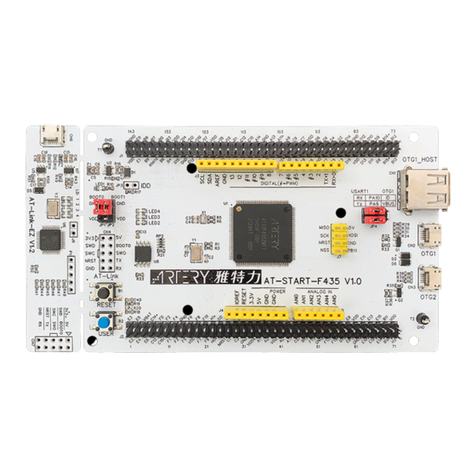
AT-Link is shown in the figure below.
Figure 1. AT-Link physical picture
1.1.2. Programming tools and software
AT programming tools and software:AT-Link/AT-Link-Pro / J-Link, ICP/ISP
Third-party programming tools:
−Xuanwei: https://xuanweikeji.taobao.com
−Maxwiz: www.maxwiz.com.cn
−ZLG: http://tools.zlg.cn/tools
−Amo: http://www.amomcu.cn
1.1.3. AT32 KEIL and IAR development environment
①For Keil compiling system, it is recommended to use Keil 4.74, 5.23 or above.
You need to install the Pack and add theAT32 MCU part numbers in the Keil. The pack is
available from Artery website.
For Keil_v5 version, Keil.AT32F4xx_DFP needs to be installed;
For Keil_v4 version, Keil_AT32F4xx_AddOn is needed;
By default, Keil installation path can be automatically recognized, if failed or incorrect, you need
to manually select Keil installation path.
Rev 1.02
www.arterytek.com

AT32F403 Application note
2020.8.20 6
Figure 2. Install the Keil.AT32F4xx_DFP
Figure 3. Install the Keil_AT32F4xx_AddOn
WhenAT-Link is used in Keil environment, select “CMSIS-DAP debugger “in “Debug”.
Figure 4. Keil Debug option
Click on “Settings” in the “Debug” to enter “cortex –M Target Driver Setup” dialogue box shown
below:
1. Select “AT-Link-CMSIS-DAP”;
2. For Port, select “SW”, then tick “SWJ”
3. ARM SWD debug module is recognized.
Figure 5. Keil Debug settings
Rev 1.02
www.arterytek.com

AT32F403 Application note
2020.8.20 7
In “Utilities”, you need to first uncheck the “Use Debug Driver” option, select the “CMSIS-DAP
Debugger” from the drop-down menu, and then tick the “Use Debug Driver” option (you need to
first uncheck, and then tick it)
Figure 6. Keil Utilities option
②For IAR compiling system, it is recommended to use IAR 7.0, IAR 6.1 or above.
You need to install the Pack and add theAT32 MCU part numbers in the LAR. The pack is
available from Artery website.
The IAR_AT32F4xx_AddOn needs to be installed. By default, the LAR installation path can be
automatically recognized, if failed or incorrect, you need to manually select LAR installation
path.
Figure 7. Install the IAR_AT32F4xx_AddOn
WhenAT-Link is used in IAR environment, select “CMSIS-DAP” in “Debugger”.
Figure 8. IAR Debug option
Rev 1.02
www.arterytek.com

AT32F403 Application note
2020.8.20 8
Figure 9. IAR CMSIS-DAP option
③At present, in IAR compiling environment, the Pack does not support bank 3 operations
(external SPI Flash via SPIM interface); If bank3 is needed, please compile it in the Keil
environment.
④Selection of BSP and PACK (six scenarios are described as below)
Table 1. Selection of BSP and PACK
No.
BSP/Pack used
Whether to use
AT32F403 new features
Solutions
1
AT32F403 BSP/Pack
Y
Refer to the BSP related routines
2
SXX32F103
BSP/Pack
N
1.When the HSERDY flag becomes 1, add a delay of
2mS;
2.When the system clock status switches from
SYSCLKSTS to PLL, add a delay of 200uS;
3. Modify the corresponding program according to
3.4 peripheral differences in the migration guide from
SXXF103 to AT32F403.
3
SXX32F103 register
operations
N
1.When the HSERDY flag becomes 1, add a delay of
2mS;
2.When the system clock status switches from
SYSCLKSTS to PLL, add a delay of 200uS;
3. Modify the corresponding program according to
3.4 peripheral differences in the migration guide from
SXXF103 to AT32F403.
4
SXX32F103 BSP +
AT32 Pack
N
1.When HSERDY flag becomes 1, add a delay of
2mS;
2.When the system clock status switches from
SYSCLKSTS to PLL, add a delay of 200uS;
3.Modify the FPU settings;
4. Modify the corresponding program according to
3.4 peripheral differences in the migration guide from
Rev 1.02
www.arterytek.com

AT32F403 Application note
2020.8.20 9
SXXF103 to AT32F403.
5
SXX32F103 register
operations
Y
1.When the HSERDY flag becomes 1, add a delay of
2mS;
2.When the system clock status switches from
SYSCLKSTS to PLL, add a delay of 200uS;
3. Modify the corresponding program according to
3.4 peripheral differences in the migration guide from
SXXF103 to AT32F403.
6
SXX32F103
BSP/Pack
Y
1.When the HSERDY flag becomes 1, add a delay of
2mS;
2.When the system clock status switches from
SYSCLKSTS to PLL, add a delay of 200uS;
3. Modify the corresponding program according to
3.4 peripheral differences in the migration guide from
SXXF103 to AT32F403.
For detailed information on BSP and Pack, please refer to AT32F4xx BSP & Pack Application note,
which is located in the AT32F4xx_StdPeriph_Lib_V1.x.x folder available from Artery website.
Note: becauseAT32F403has different Flash mechanism from SXX, there is no need to set the following two
Flash wait bits for AT products:
Figure 10. SXX Flash wait bits
This means that the SXX Flash needs to wait for 1-2 clocks at high speed to fetch instructions,
but AT has no such restriction.
Rev 1.02
www.arterytek.com

AT32F403 Application note
2020.8.20 10
1.1.4. How to quickly replace SXX
Step 1: De-solder SXX32F103 and replace it with the corresponding AT32F403 part
according to the peripheral specifications, Flash size, SRAM size, etc.
Step 2:Add at least 2ms of delay after reading RCC->CR.HSERDY, and add at least 200us
of delay after reading RCC->CR.PLLRDY
Step 3: Download SXX32F103 HEX file or BIN file using Artery ICP, ISP or KEIL/ IAR
Step 4: If necessary, download information other than SXX32F103HEX file or BIN file or
perform system calibration
Step 5: Check if the program can run normally
Step 6: For other issues, please refer to Migration guide from SXX32F103 to AT32F403
Step 7: If the program still cannot work normally after following the above steps, please refer
to other chapters in this document, or contact your agent for assistance.
Note: Since AT32F403 applies a flexible memory extension design, the internal Flash
memory has a non-zero wait area, which will cause some SXX32F103 programs to run poorly
on AT32F403.
For how to improve operating efficiency, please refer to AN0004_Performance_Optimization_
Optimization V1.0.x.pdf.
1.2. Enhanced functions of AT32F403
1.2.1 PLL setting when the clock is greater than 72 MHz
AT32F403 embeds a PLL that can output up to 200 MHz clock, the setting is slightly different.
Thus the PLLRANGE register must be configured depending on the output frequency, that is,
PLLRANGE=1 when greater than 72 MHz, and PLLRANGE=0 when less than or equal to 72
MHz.
SXX32F103 PLL setting example: (HSE=8MHz, PLL=72MHz)
RCC->CFGR |= (uint32_t)(RCC_CFGR_PLLSRC_HSE | RCC_CFGR_PLLMULL9);
AT32F403 PLL setting example: (HSE=8MHz)
#define RCC_CFG_PLLRANGE_LE72MHZ ((uint32_t)0x00000000)
/*!< When PLL frequency is less than or equal to 72MHz */
#define RCC_CFG_PLLRANGE_GT72MHZ ((uint32_t)0x80000000)
/*!< When PLL frequency is greater than 72MHz */
PLL=72MHz:
RCC->CFG|=(uint32_t)(RCC_CFG_PLLRC_HSE| RCC_CFG_PLLMULT9 |
RCC_CFG_PLLRANGE_LE72MHZ);
PLL=200MHz:
RCC->CFG|=(uint32_t)(RCC_CFG_PLLRC_HSE|RCC_CFG_PLLMULT25
|RCC_CFG_PLLRANGE_GT72MHZ);
Rev 1.02
www.arterytek.com
AT32F403 Application note
2020.8.20 11
1.2.2 How to enable FPU (Hardware Floating Point Unit)
There are two situations in Keil environment as follows:
①Use AT32F403 BSP/Pack or the modified SXX BSP/Pack to select “Floating Point Hardware”
as shown below:
Figure 11. Enable FPU in Keil environment
②Because SXX32F10X series does not support FPU function, if users want to enable FPU in
the project developed under SXX library, the following procedures are required:
A. Firstly, refer to AT32F4xx standard library BSP and Pack Application note to install Keil
environment Pack, and modify related header files.
B. Then, select the corresponding AT parts, and select in “Options for Target” as shown below:
Figure 12. Enable FPU in Keil environment
C. Finally, add the following configuration in the SystemInit function of the
system_stm32f10x.c, and add cm4.h to the project.
Figure 13. Add a code to enable FPU in Keil environment
Rev 1.02
www.arterytek.com
AT32F403 Application note
2020.8.20 12
There are also two situations in IAR environment as follows:
①UseAT32F403 BSP/Pack or the modified SXX BSP/Pack to modify the Floating Point
Hardware as shown below:
Figure 14. Enable FPU in IAR environment
②Because SXX32F10X series does not support FPU function, if users want to enable FPU in
the project developed under SXX library, the following procedures are required:
Firstly, refer to AT32F4xx standard library BSP and Pack Application note to install IAR
environment Pack, and modify related header files.
Then, select the correspondingAT parts, and select in “General Options---Target” as shown
below:
Finally, add the following configuration in the SystemInit function of the system_stm32f10x.c,
and add cm4.h to the project.
Figure 15. Add a code to enable FPU in IAR environment
Rev 1.02
www.arterytek.com
AT32F403 Application note
2020.8.20 13
1.2.3 Configuration for AT32F403 ZW/NZW Flash and embedded SRAM size
Except forAT32F403CBT6, other products support the allocation of internal Flash memory and
SRAM through Option Bytes configuration. Taking AT32F403RET6 as an example, the internal
Flash memory and SRAM can be configured as follows:
- ZW: 256 KB, NZW: 768 KB, SRAM: 96 KB (Factory default);
- ZW: 128 KB, NZW: 896 KB, SRAM: 224 KB
The core reads the instruction code stored in the zero-wait Flash without any delay, and it does
not need to insert a wait clock because the CPU frequency is so fast that Flash cannot keep up
with it.Assuming the system clock is 200 MHz, the AT32F403 has 256 KB of zero wait. The first
256 KB of the 512 KB bin file can be executed at 200 MHz, and the last 256 KB bin file is stored
in the non-zero wait area with the execution rate of 80 MHz, which is still faster than the max
frequency 72 MHz of SXX32F10X. The operating rate of non-zero wait is 0.4 times of that of
zero wait.
The embedded SRAM 96 KB (default) /224 KB can be selected in one of the following
ways:
TheAT32F403 SRAM size configuration involves the FMC option bytes, which is selected by
configuring the EOPB0. The address is 0x1FFF_F810.
EOPB0=0xFF means that the on-chip SRAM is 96 KB, while, EOPB0=0xFE for 224 KB of
SRAM and EOPB0=0x3 for 32 KB of SRAM.
It must be powered down or reset once to enable the EOPB0.
Rev 1.02
www.arterytek.com

AT32F403 Application note
2020.8.20 15
Artery ISP Programmer tool
Enter the final interface, select “96 KB/224 KB”---“Apply to device”
Figure 18. ISP tool option bytes select SRAM size
Artery ISP Multi-Port Programmer
Click on “Download option byte file”---“Edit”---select “96 KB/224 KB”---“Save to file” (create
a new option byte programming file)---“Close”---“Begin”, or click on “Download option byte file”---
“Open” (open the saved option byte programming file)---“Begin”
Figure 19. ISP Multi-Port Programmer option bytes operation
Rev 1.02
www.arterytek.com
AT32F403 Application note
2020.8.20 16
②Users can also modify SRAM size in the Bootloader program (IAP), as shown in the example
below:
void Extend_SRAM(void)
{
// check if RAM has been set to 224K, if not, change EOPB0
if(((UOPTB->EOPB0) & 0xFF) != 0xFE)
{
/* Unlock Option Bytes Program Erase controller */
FLASH_Unlock();
/* Erase Option Bytes */
FLASH_EraseUserOptionBytes();
/* Change SRAM size to 224KB */
FLASH_ProgramUserOptionByteData((uint32_t)&UOPTB->EOPB0,0xFE);
NVIC_SystemReset();
}
}
Rev 1.02
www.arterytek.com
AT32F403 Application note
2020.8.20 17
③Configure theAT32F403 SRAM to 224KB in the startup file
SRAM will be loaded when the startup file is running. If the program has no IAP, but the SRAM used
by the application is greater than 96 KB, the loading will fail and enter the hardfault, which will cause
the application to fail to run. Thus, you can configure the SRAM size to be 224 KB before loading
the SARM in the startup file.Add the following red code to the startup files in Keil compilation
environment:
; Reset handler
Reset_Handler PROC
EXPORT Reset_Handler [WEAK]
IMPORT __main
IMPORT SystemInit
IMPORT Extend_SRAM
MOV32 R0, #0x20001000
MOV SP, R0
LDR R0, =Extend_SRAM
BLX R0
MOV32 R0, #0x08000000
LDR SP, [R0]
LDR R0, =SystemInit
BLX R0
LDR R0, =__main
BX R0
ENDP
Add the following red font in the startup file in IAR environment
; Default interrupt handlers.
THUMB
PUBWEAK Reset_Handler
SECTION .text:CODE:REORDER:NOROOT(2)
EXTERN Extend_SRAM
Reset_Handler
MOV32 R0,#0x20001000
MOV SP,R0
LDR R0,=Extend_SRAM
BLX R0
MOV32 R0,#0x08000000
LDR SP,[R0]
LDR R0, =SystemInit
BLX R0
LDR R0, =__iar_program_start
BX R0
Rev 1.02
www.arterytek.com

AT32F403 Application note
2020.8.20 18
Add declaration and define the Extend_SRAM function in the application
void Extend_SRAM(void)
{
// check if RAM has been set to 224K, if not, change EOPB0
if(((UOPTB->EOPB0) & 0xFF) != 0xFE)
{
/* Unlock Option Bytes Program Erase controller */
FLASH_Unlock();
/* Erase Option Bytes */
FLASH_EraseUserOptionBytes();
/* Change SRAM size to 224KB */
FLASH_ProgramUserOptionByteData((uint32_t)&UOPTB->EOPB0,0xFE);
NVIC_SystemReset();
}
}
Note: It is not recommended to use APP to change the SRAM size; if the SRAM space used in APP is
greater than the modified SRAM size, the program will enter a Hardfault.
Rev 1.02
www.arterytek.com
AT32F403 Application note
2020.8.20 19
1.2.4 Encryption (read protection and external Flash encrypted)
1.2.4.1 Read protection
Read protection, commonly referred to as “encryption”, acts on the entire Flash memory area.
Once the read protection is set in the Flash, the embedded Flash storage area can only be read
through the normal execution of the program instead of JTAG or SWD.
When the read protection is disabled using ISP/ICP tool, the chip will erase the Flash.
ISP/ICP tool can be used to enable/disable read protection as follows:
ICP tool
Read protection: click on “target”--- “read protection”--- “enable protection”
Disable read protection: click on “target”---“read protection”--- “disable read protection”
Artery ISP Programmer
Read protection: click on “Enable/Disable protection”--select “Enable---read protection”--“Next”-
“Yes”, and the program is encrypted.
Figure 20. ISP enable read protection
Rev 1.02
www.arterytek.com
AT32F403 Application note
2020.8.20 20
Disable read protection: click on “enable/disable protection”---select “disable-read protection”---
“Next”—“Yes”, and then the Flash can be unencrypted.
Figure 21. ISP disable read protection
Artery ISP Multi-Port Programmer
Read protection: click on “enable/disable protection”---select “enable-read protection”---click
“Begin”, and then the program is encrypted.
Figure 22. ISP Multi-Port Programmer enable read protection
Rev 1.02
www.arterytek.com
Table of contents
Other ARTERY Microcontroller manuals

ARTERY
ARTERY AT32 Installation and operating instructions

ARTERY
ARTERY AT32F435 Series Guide

ARTERY
ARTERY AT32F415 Series User manual

ARTERY
ARTERY AT-START-F435 User manual

ARTERY
ARTERY AT32F421 GPIO User manual

ARTERY
ARTERY AT32F421C8T7 User manual

ARTERY
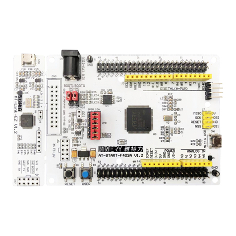
ARTERY AT-START-F403A User manual

ARTERY
ARTERY AT32F421 Series User manual
Popular Microcontroller manuals by other brands

mikroElektronika
mikroElektronika ROTARY R click quick start guide

NEC
NEC mPD780024AS Series Preliminary user's manual

Silicon Laboratories
Silicon Laboratories C8051T60x-DK user guide

mikroElektronika
mikroElektronika CLICKER 2 FOR FT90X manual

NEC
NEC mPD17120 Subseries user manual

Intrinsyc
Intrinsyc Open-Q 626 mSOM quick start guide