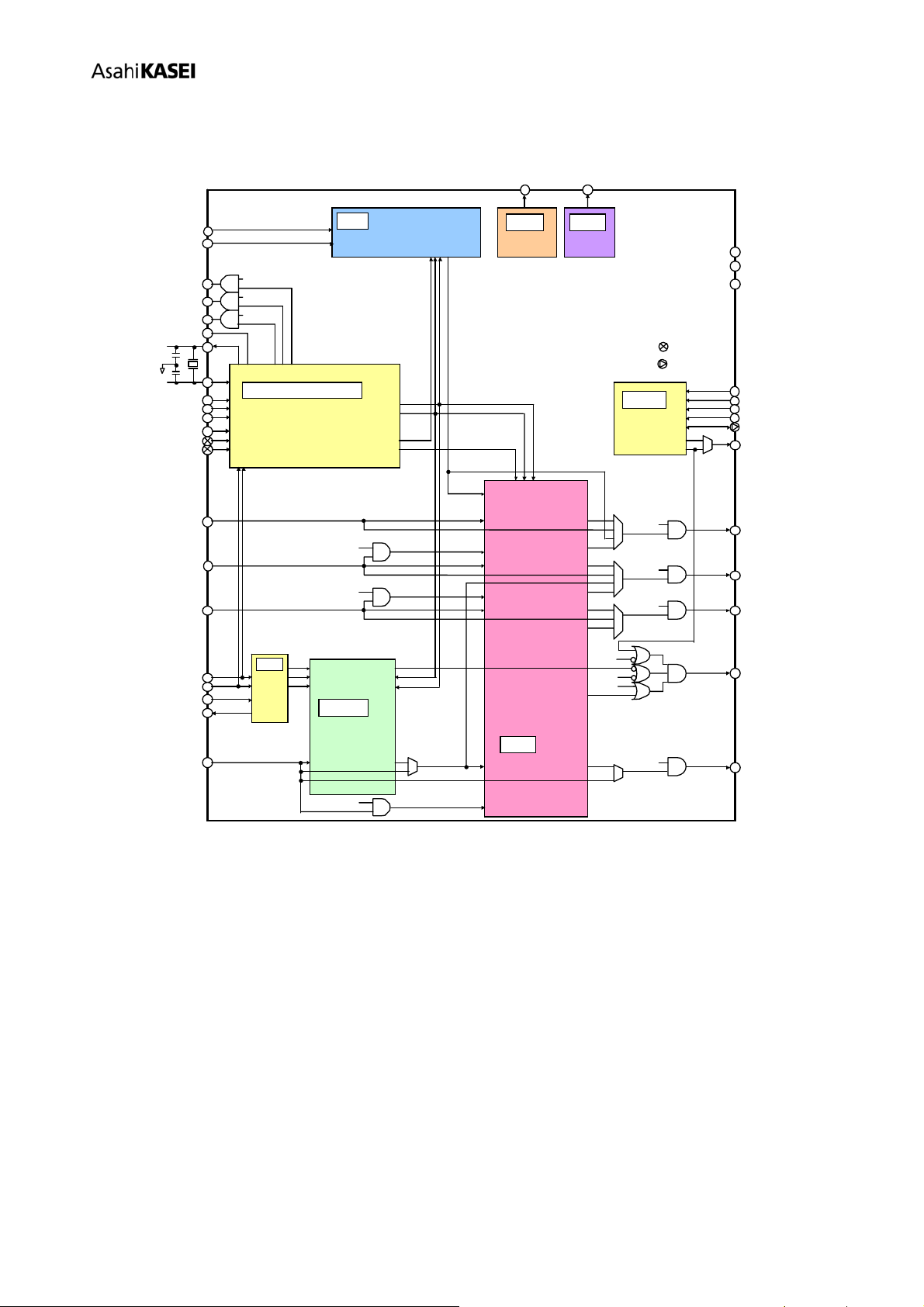
[AK7734]
MS1033-E-03 - 6 - 2010/06
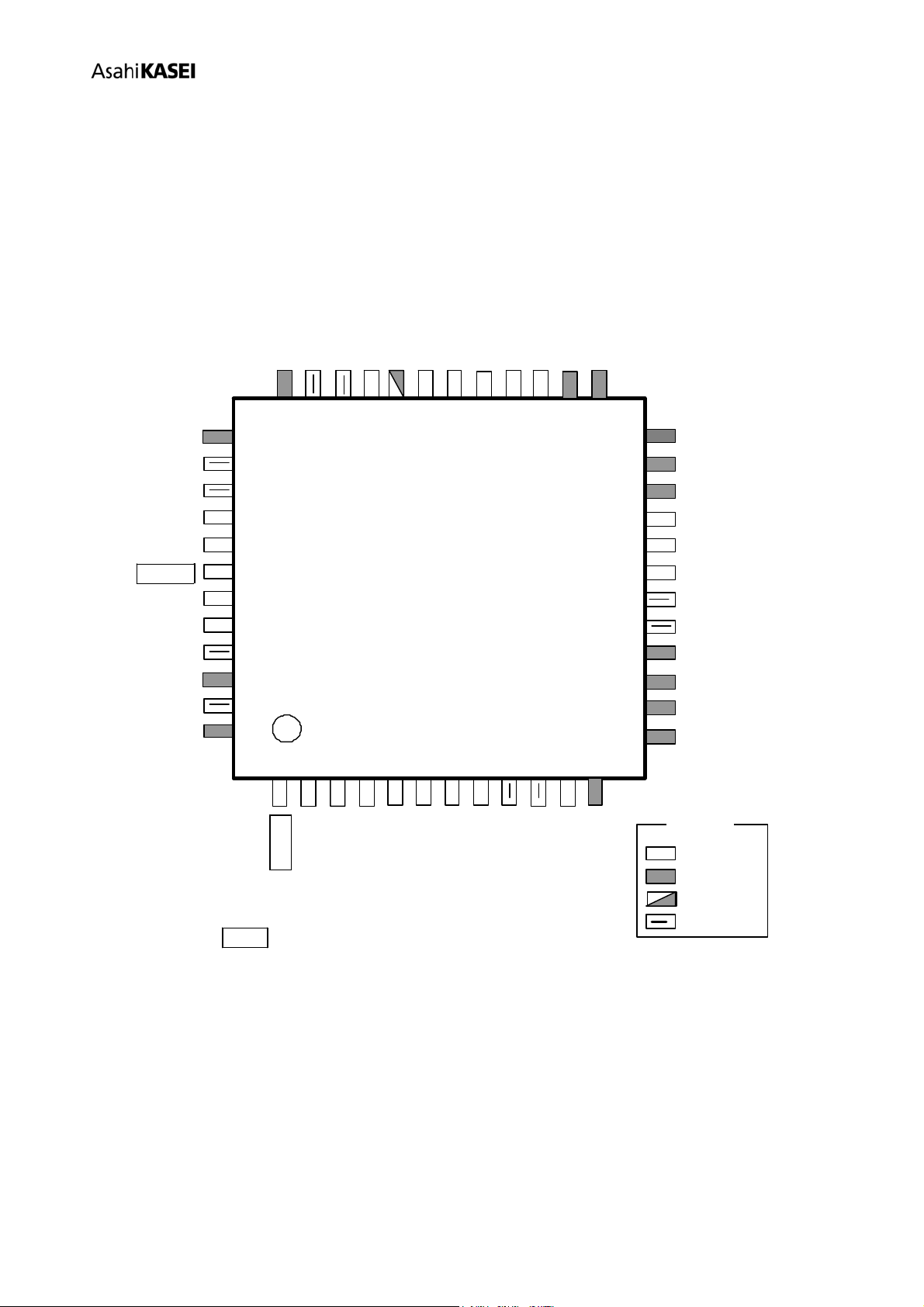
No. Name I/O Function Classification
1 TESTI1 I Test1 Pin (Internal pull-down)
This pin must be connected to VSS. Test
2 CKM[2] I Clock Mode Select Pin2 Mode Select
3 CKM[1] I Clock Mode Select Pin1 Mode Select
4 SDIN1 I Serial Data Input Pin1 Digital Input
JX0 I
Conditional Jump Pin0
A conditional jump pin (JX0) is available by setting control register (JX0E) to
“1”.
Conditional Input
5
SDIN2 I Serial Data Input Pin2 Digital Input
JX1 I
Conditional Jump Pin1
A conditional jump pin (JX1) is available by setting control register (JX1E) to
“1”.
Conditional Input
6
SDIN3 I Serial Data Input Pin2 Digital Input
7 BITCLKI1 I Serial Bit Clock Input Pin1
Normally connected to the Bluetooth Data Clock line (256kHz/512kHz). System Clock
8 LRCLKI1 I LR Channel Select Clock Pin1
Normally connected to the Bluetooth LR Clock line (8kHz). System Clock
9 DVDD - Power Supply for Digital Section 3.0V ~ 3.6V Digital
Power Supply
10 VSS1 - Ground Pin 0V Power Supply
11 XTI I
Crystal oscillator input pin
Connect a crystal oscillator between this pin and the XTO pin, or input an
external clock to the XTI pin.
Clock
12 XTO O
Crystal oscillator output pin
When a crystal oscillator is used, connect it between XTI and XTO. When an
external clock is used, leave this pin open. During initial reset, the output of
this pin is not determinable.
Clock
13 SDOUT4 O Serial Data Output Pin4
Outputs “L” during initial reset. Digital Output
14 SDOUT3 O Serial Data Output Pin3
Outputs “L” during initial reset. Digital Output
15 SDOUT2 O Serial Data Output Pin2
Outputs “L” during initial reset. Digital Output
16 SDOUT1 O Serial Data Output Pin1
Outputs “L” during initial reset. Digital Output
17 VSS2 - Ground Pin 0V Power Supply
18 DVDD - Power Supply for Digital Section 3.0V ~ 3.6V Digital
Power Supply
19 I2CSEL I
I2C BUS Select Pin (Internal pull-down)
I2CSEL pin = “L”: 4-wired Interface
I2CSEL pin = “H”: I2CBus selected mode. SCL and SDA are active.
I2CSEL should be connected to “L” (VSS) or “H” (DVDD).
I2C Select
20 INITRSTN I
Reset Pin (for initialization)
Use to initialize the AK7734. When changing CKM [3:0] and changing XTI
or BITCLK input frequency, it is necessary to set this pin.
Reset
21 CKM[0] I Clock Mode Select Pin Mode Select
22 LRCLKO O LR Channel Select Clock Pin
Outputs “L” during initial reset in master mode.
System Clock
Output
PIN FUNCTION