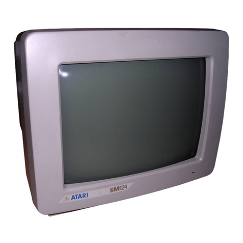
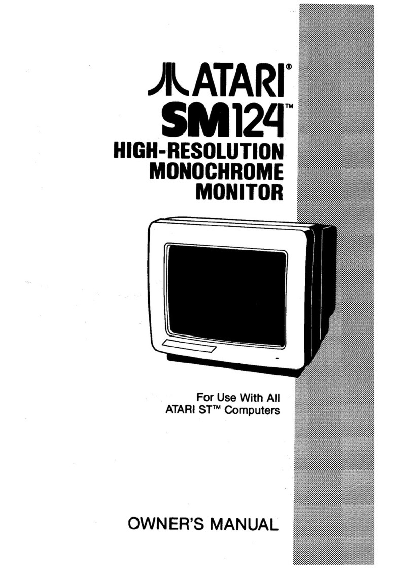
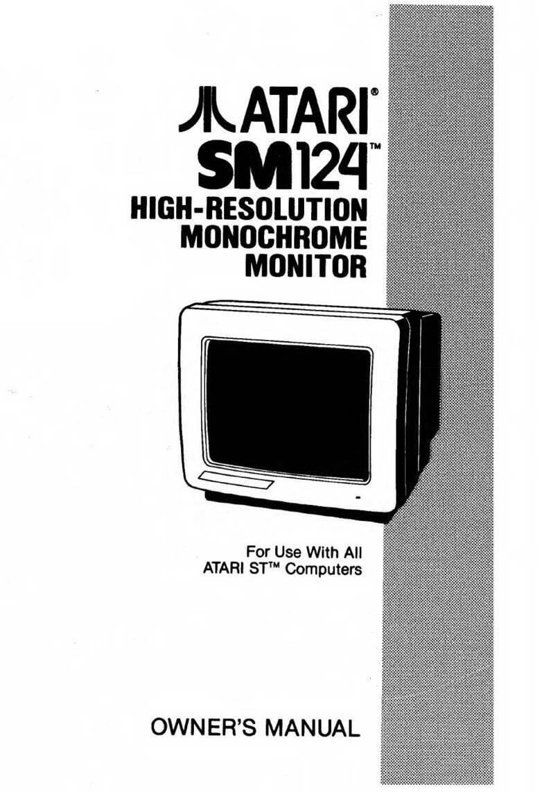
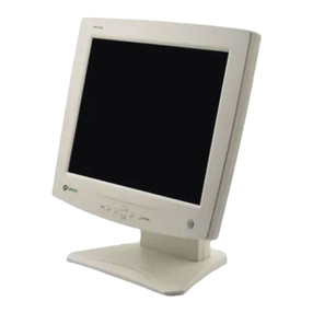
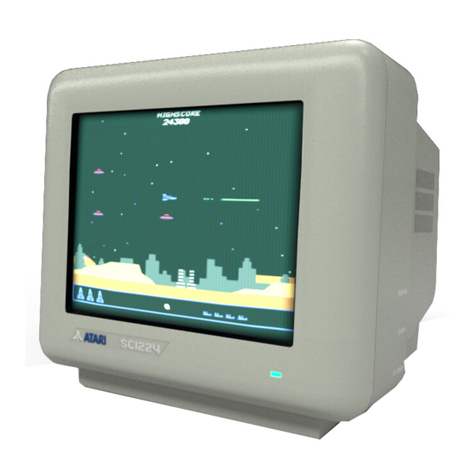
Atari SM124 User manual

chaltungsdienst
Lange
ruil-Dlagrom-Soivice
in
Getmony
•
•
D-liX)0
Berlin
nl
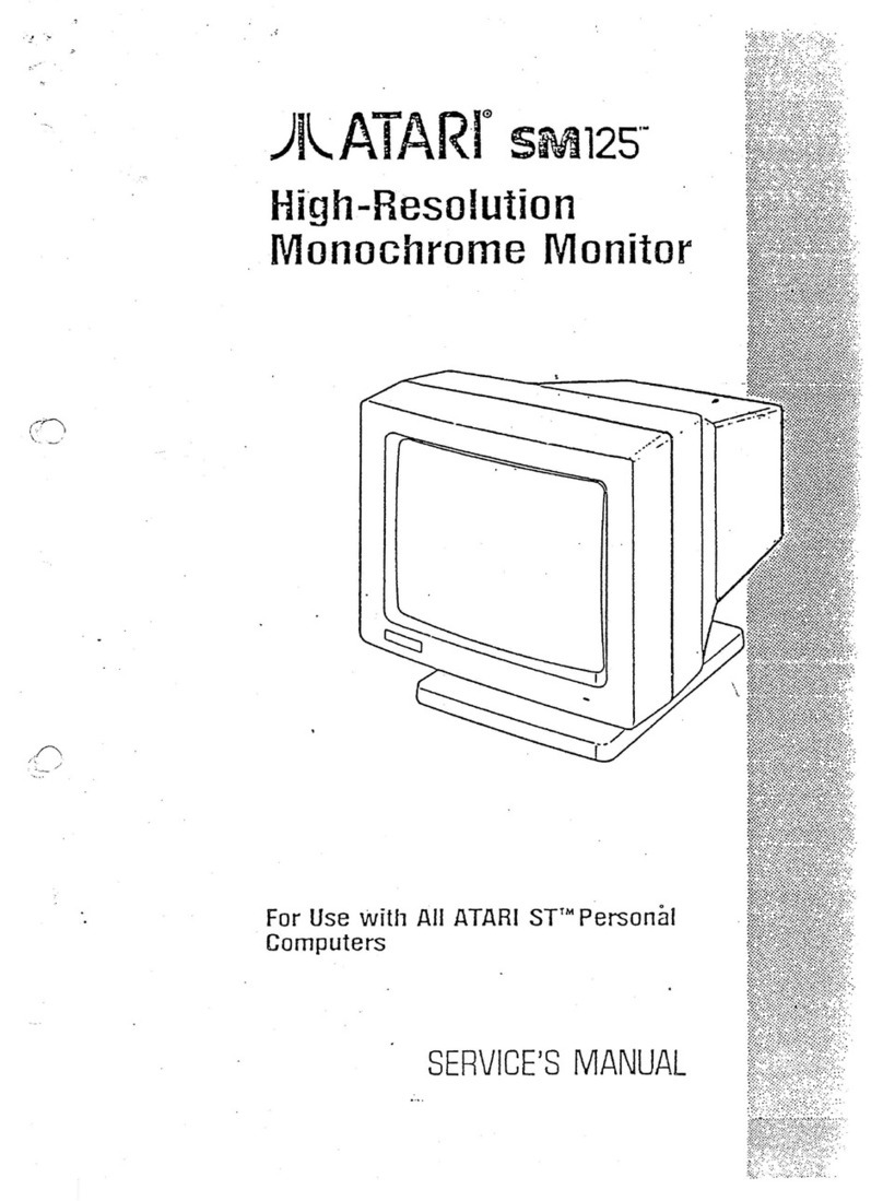
HIGH-RESOLUTION
MONOCHROME MONITOR
CONTENTS
SAFETY PRECAUTIONS
SPECIFICATIONS
ADJUSTMENT AND MAINTENANCE
THEORY OF OPERATION
3LOOK DIAGRAM
TIMING CHART
TRANSISTOR &1C BASING
VOLTAGE CHART
COMPONENT OF P.C.B
TROUBLESHOOTING CHART
REPLACEMENT PARTS LIST
exploded view
SCHEMATIC DIAGRAM
SERVICE MANUAL

SAFETY PRECAUTIONS
Operation of the monitor outside of its cabinet or with its back
removed involves ashock hazard. Work on these models should
only be performed by those who are thoroughly familiar with
precautions necessary when working on high voltage equipment.
Exercise care when servicing this chassis with power applied.
Many Bplus and video input terminals are exposed which, if
carelessly contacted, can cause serious shock or result in damage
to the chassis. Maintain interconnecting ground lead connec-
tions between chassis, picture tube dag and power PWB earth
when operating chassis.
Certain HV failures can increase X-ray radiation. The monitor
should not be operated with HV levels exceeding the sp>ecified
rating for their chassis type. The maximum operating HV
specified for the chassis used in these receivers is 12 KV -f 1
—2KV at zero beam current with aline voltage of 220V AC.
Higher voltage may also increase possibility of failure in HV
supply.
It is important to maintain specified values of all components
in the horizontal and high voltage circuits and anywhere else
in the monitor that could cause arise in high voltage or
operating supply voltages. No changes should be made to the
original design of the monitor.
Components shown in the shaded areas on the schematic
diagram and/or identified by an Sin the replacement parts list
should be replaced only with exact Factory reconunended
replacement parts. The use of unauthorized substitute parts may
create ashock, fire. X-radiation, or other hazard.
To determine the presence of high voltage, use an accurate, high
impedance, HV meter connected between second anode lead
and the CRT dag grounding device. When servicing the High
Voltage System, remove static charge by connecting alOK ohm
resistor in series with an insulated wire (such as atest probe)
between picture tube dag and 2nd anode lead. (Before AC line
cord is disconnected from AC supply).
The picture tube used in this monitor employs integralimplo-
sion protection. Replace with tube of the same type numbe)
for continued safety. Do not lift picture tube by the neck. Handle
the picture tube only when wearing shatter-proof goggles and
after discharging the high voltages completely. Keep others
without shatter-proof goggles away.
SAFETY INSPECTION
Before returning the monitor to the user, perform the follow-
ing safety checks;
PROTECT YOUR CUSTOMER
1.
Inspect all wire harmless assemblies to make certain that
the wires are not pinched or that any between hardware is
not lodged between the chassis and other metal parts in the
monitor.
2. Replace all protective devices such as non-metallic control
knobs, insulating fishpapers, cabinet backs, adjustment and
compartment covers or shields, isolation resistor-capacity!
networks, mechanical insulators, etc.
|
3. To be sure that no shock hazard exists, acheck for the
presence of leakage current should be made at each exposed
metal part having areturn path to the chassis (input terminal,
cabinet metal, screw heads, knobs and/or shafts, escutcheon, ^
etc.) in the following manner.
|
Plug the AC line cord directly into a220V AC receptacle.'
(Do not use an Isolation Transformer during these checks.)
All checks must be repeated with the AC line cord plug con-
nections reversed. (If necessary, anonpolarized adapter plug
must be used only for the purpose of completing these
checks.)
If available, measure current using an accurate leakage current
tester. (Use Standard Equipment Item No. 21641 .)Any reading I
of 0.26 Aor more is excessive and indicates apotential shock
hazard which must be corrected before returning the monitor
to the owner.
If areliable leakage current tester is not available, an alternate
method of measurement should be used. Using two clip leads,
connect a1.5K ohm, 10 watt resistor in parallel with a0.15MF
capacitor in series with aknovsTi earth ground. Use aVTVM
or VOM with 1000 ohms per volts sensitivity, or higher to
measure the AC voltage drop across the resistor. Any reading
of 0.35 volt RMS or more is excessive and indicates apotential
shock hazard which must be corrected before returning the
monitor to the owner.
Fig. 1, Voltmeter Hook-up for Safety Check
-2-
SPECIFICATIONS
1. CATHODE RAY TUBE
Type; Non-glare DARK
Size &Deflection angle; 12", 90°
Neck diameter; 20 mm
Phosphor: Paper White
2. INPUT
Input signal: TTL Signal
•Video :1Vp-p Positive
•Audio :1Vp-p
•V’ertical Drive :5±1.5 Vp-p Negative
•Horizontal Drive :5±1.5 Vp-p Negative
Power Input :AC 220V 50Hz, 0.3A
Input Connector :13 Pin Din Connector
3.SCANNING
Horizontal frequency ;35.7 KHz
Horizontal retrace time :6.3 uS
Vertical frequency ;71.2 Hz
Vertical retrace time ;420 uS
4. VIDEO
•Display Area (HXV) :210 mm X130 mm
•.Amplifier Type ;Linear
•Frequency band width ;32 MHz
•Horizontal resolution :1100 lines at center
•Display character :80 X50 characters
5. GEOMETRIC DISTORTION: 2.5% max.
6. LINEARITY
•Horizontal :10% max.
•Vertical: 10% max.
7. EXTERNAL CONTROLS: BRIGHTNESS, CONTRAST,
ON/VOLUME.
ADJUSTMENT AND MAINTENANCE
CIRCUIT PROTECTION
Circuit protection is provided by one Mini fuse, on the power
pc boa.;-d. A1.6 Ampere fuse (F901) is wired into one side of the
AC line and provides primary protection to the entire chassis.
1. CENTERING ADJUSTMENT
CAUTION: The following adjustment points are close to
the high voltage yoke terminal. If the raster is
not centered in the raster opening, it m^ay be
centered by removing the cabinet back and ad-
justing the centering tabs on the neck of the
tube, located at the rear of the deflection yoke.
Turn the whole device clockwise or counter-
clockwise. To increase the amount of raster
shift, move the two tabs which project from
the device, farther apart. If the raster is tilted
on an angle, it m.ay be straightened by loosen-
ing the deflection yoke locking clamp and
rotating the deflection yoke.
2. FOCUS
Adjust the foucs control (\fl^703) for best overall focus of the
lest pattern (marked with the symbol ''%"). Usually the center
and comers of the screen do not focus at the same setting and
acompromise must be made.
3. BRIGHTNESS
Adjust subbrightness control (\T^701) for visual cut off of the
raster when external brightness is turned to maximum.
4. VERTICAL SIZE ANT) LINEAR ADJUSTMENT
The vertical size control (VT601) should be adjusted for the
picture to fill the screen vertically, the linear control (\T602)
should be adjusted for best overall vertical linear. Adjustment
of either control will not affect the adjustment of the other.
5.
HORIZONTAL SIZE ANT) LINEAR ADJUSTMENT
The horizontal size control (L703) is on the main PCB, it should .
be adjusted for the picture to fill the screen horizontally, the
linear control (L704) should be adjusted for the best overall
horizontal linear adjustment so neither control will affect the
adjustment of the other.
6.
B+ ADJUSTMENT
B"*" adjustment control (\T^901) is located on the main PCB
and it should be adjusted for the FBT input voltage and other
circuit voltage and B"*" adjustment control (VR901) should be’
set to DC 27V.
-3-


THEORY OF OPERATION
1. VIDEO AMPLIFIER
The Fig. 3details the cascade video amplifier. Video amplifica-
tion is provided by the Q304 and Q305. Q304 and Q30S are
connected in acascade configuration. Q304 operates as acom-
mon emitter and Q305 operates in the common base con-
Hguration. This minimized the miller effect input capacitance
and the defining breakdown parameter for Q304 which
becomes BVCBO as opposed to BVCEO.
This enables selection of ahigher speed/ower breakdov^-n tran-
sistor to be used in the video amplifier.
The emitter of Q305 is driven by the collector of Q304 which
is ahigh frequency transistor. Overall voltage gain for the
stage is determined by the ratio of R313.314, 315,316, 317
to R311.
2. VERTICAL DEFLECTION
The vertical deflection circuit consists of an 1C TDA1170D
and the vertical deflection coil of the DY (and associated cir-
cuitry). The 1C TDA1170D incorporates all the functions for
providing the yoke of the MONITOR with the current re-
quired for vertical deflection.
The preamplifier is ahigh input impedance differential type,
with inverted input available at pin 1.
The non-inverting input is fixed internally in the circuit at a
stabilized voltage of approximately 2.2V. During flyback, the
flyback generator produces avoltage equal to approximate-
ly double the supply voltage, and this is applied at the yoke
by means of the power Amplifier. The oscillator is athreshold
type with ahigh degree of frequency stability. It is synchroniz-
ed with acircuit which receives either positive or negative
sync pulses and ensures complete immunity from noise
throughout most of the scanning time.
Fig, 3Video Amplifier

Fig. 4, Block Diagram of the TDA 1170D
3. HORIZONTAL DEFLECTION
Horizontal deflection 1C, AN5790 (IC701), oscillates freely
on condition that the external voltage source is applied to it.
Horizontal-oscillation frequency' is made by internal oscilla-
tion after H-SYNC has been applied to the pin 1of horizon-
tal deflection IC, AN5790N (IC701).
Drive pulse of the output pin 8, of H-deflection 1C, AN5790N’,
is applied to the base pin of Q701.
FBT deflects horizontally when the inverted pulse is applied
to the base of H-output TR (Q702).

\
Fig. 6, Block Diagram of the TDA-i6Cl
POWER SUPPLY DESCRIPTIONS
This SMPS (switching mode power supply) using TDA4601 ob-i
tains rectified DC 27V, 12V from AC220V. j
Power is supplied in the following procedure: i
1) AC220V supplied from the AC Line is rectified by D901. '
2) Rectified voltage is supplied to the T901. As to TDA4601.
Voltage which is primarily rectified by D901, is supplied to
pin 9of IC901 through R904.
3) At this moment, apulse is generated at pin 7 of the 1C901
which switches (^901 by internal oscillation of 1C901.
4) This oscillation causes Q901 to switched, and at the secon-
dary terminal of T901, avoltage proportional to the turn ratio'
is generated.
5) The generated voltage supplies DC 27V, 12V to the output
terminal after the rectified by D930, D931 and filtered by C931,
C934 and L931, L933.
6) Between Pins 5and 6of T901, avoltage is generated propor-
tional to turn the ratio from voltage generated between Pins
4and 3.
7) Defecting voltage (pin 6of IC901) is obtained through D904
by generated voltage.
5) Stable voltage is obtained by changing internal oscillation
integer.
4. POWER SUPPLY
The power supply is aSMPS (switching mode power supply)
that consists of switching 1C901 (TDA4601), SMPS trans-
former (T901), and the associated components. The basic
ytheory of the SMPS is the circuit of self oscillation. The
primary winding of the SMPS transformer is applied the pulse
by operating (2901 Therefore, rectified DC 27V and DC 12V
is obtained by D930, D931 in the secondary winding of SMPS
transformer T901.
PIN CONTIGURATION
Pin No. IFunction
Vref output
Zero crossing identification
Input controlled amplifier, overload amplifier
Collector current simulation
Connection for additional protective circuit
Ground (rigidly connected to substrate mounting
plate)
DC output for charging the coupling capacitor
Pulse output —driving of the switching
transistor
Supply voltage
/

TO FIT
K27V
-8-
1

BLOCK DIAGRAM

10

/
TRANSISTOR &IC BASING
<v
REFERENCE
NO. FIGURE DESCRIPTION
0701: RD11EB2
i
D704^ RGP30G
RGPIOD
RGP10G
LEO SLP262B
0707; i>=! ERG26-20
0303,0401
0402,0403
0701
1
!
E
KTC1959
KTA562TM
KTC200
D601,D702,D703
D705,0706,0708
0906

VOLTAGE CHART
TR NO. TYPE FUNCTION INPUT CONDITION BEc
Q301 2N2369 VIDEO INPUT NO SIGNAL 0 0 3.8
iVp-p VIDEO SIGNAL 0.8 0 3.4
Q302 2N2369 VIDEO AMP NO SIGNAL 0.8 0 0.1
iVp-p VIDEO SIGNAL 0.8 07.2
Q303 KTC1959 BRIGHT/CONTRAST NO SIGNAL 8 7 12
ADJUSTMENT iVp-p VIDEO SIGNAL 8712
Q304 2N3904 VIDEO DRIVE NO SIGNAL 0.3 012
iVp-p VIDEO SIGNAL 7.2 6.7 -13
Q30S 2SCo503 VIDEO OUTPUT NO SIGNAL 12 12 60
iVp-p \TDEO SIGNAL 12 13 57
Q701 KTC200 HORIZONTAL NO SIGNAL 6.8 6.85 6.8
DRIVE iVp-p VIDEO SIGNAL 6.8 7 6.8
Q702 BU806 HORIZONTAL NO SIGNAL 6.4 0180
OUTPUT iVp-p VIDEO SIGNAL 6.4 0180
Q901 2SC3507 POWER NO SIGNAL 1.6 0510
SWITCHING iVp-p \TDEO SIGNAL 1.6 0520
Q401 KTC1959 AUDIO INTUT NO SIGNAL 0.7 00
iVp-p VIDEO SIGNAL 0.7 0 0
Q402 KTC1959 AUDIO AMP NO SIGNAL 6.6 112
iVp-p VIDEO SIGNAL 6.6 112
Q403 KTC562 AUDIO AMP NO SIGNAL 2.6 60
iVp-p VIDEO SIGNAL 2.6 60
-12 -

FUNCTION PIN NO.
VERTICAL
DERECTION
IC
AN5790N HORIZONTAL
DERECTION
IC
OPERATING CONDITION
iVp-p VIDEO SIGNAL
iVp-p VIDEO SIGNAL
iVp-p VIDEO SIGNAL
iVp-p VIDEO SIGNAL
iVp-p VIDEO SIGNAL
iVp-p VIDEO SIGNAL
iVp-p VIDEO SIGNAL
iVp-p VIDEO SIGNAL
iVp-p VIDEO SIGNAL
iVp-p VIDEO SIGNAL
iVp-p VIDEO SIGNAL
iVp-p VIDEO SIGNAL
iVp-p VIDEO SIGNAL
aVp-p VIDEO SIGNAL
iVp-p VIDEO SIGNAL
iVp-p VIDEO SIGNAL
iVp-p VIDEO SIGNAL
iVp-p VIDEO SIGNAL
iVp-p VIDEO SIGNAL
iVp-p VIDEO SIGNAL
iVp-p VIDEO SIGNAL
iVp-p VIDEO SIGNAL
iVp-p VIDEO SIGNAL
iVp-p VIDEO SIGNAL
iVp-p VIDEO SIGNAL
iVp-p VIDEO SIGNAL
IVp-p VIDEO SIGNAL
iVp-p VIDEO SIGNAL
iVp-p VIDEO SIGNAL
iVp-p VaDEO SIGNAL
iVp-p VIDEO SIGNAL
7iVp-p VIDEO SIGNAL 0
8iVp-p VIDEO SIGNAL 6.S
9iVp-p VIDEO SIGNAL 1.7
10 iVp-p VIDEO SIGNAL 2
iVp-p VIDEO SIGNAL
iVp-p VIDEO SIGNAL

COMPONENT OF P.C.B
MAIN P.C.B (CO.MPONENT SIDE)
-14 -

MAIN P.C.B (SOLDER SIDE)
-15 -

TROUBLESHOOTING CHART
-16 -

POWER CHARTI
-17 -
r

-18 -


REPLACEMENT PARTS LIST
CAUTION: Components identified by the symbol in the PARTS LIST and on the SCHEMATIC DIAGRAM have
special characteristics important to safety.
Do not degrade the safety of the set through improper servicing.
ABBREVIATIONS: Capacitors CC: Ceramic (TC), CE: Chemical, CK: Ceramic (Hi-K),
BP: Bipolor, CQ: Mylar, PE: Polyester, PP: Polypropylene
Resistors RD: Carbon Film, RS: Metal Oxide Film, SR: Semifix
(All CC and Plastic Capacitors are ±5%, 50 Volts and all resistor, ±5%, 1/8W unless otherwise noted.
S:Recommend Service Parts
REF. NO PART NO. DESCRIPTION REMARK
\RESISTOR
R30i or. 57085 RD, 0.125W. 330 ohm, ±5%
R302 or. 57051 RD. 0.1 25W. 220 ohm. ±5“'b
R303 01157063 .RD, 0.1 25W. 270 ohm. ^5%
R304 01157088 RD. 0.125V»', ^30 ohm, ^5%
R3C5 01157061 .RD. 0.1 25W, 220 ohm, ±5%
R307 01157075 RD. 0.125W. 120 ohm, ±5%
R308 01157065 RD. 0.1 25W, 47 ohm, ±5%
R309 01157084 RD, 0.1 25W, 300 ohm. ±5%
R310 01157071 RD. 0.1 25W, 62 ohm, ±5%
R311 01157075 RD. 0.1 25W, 120 ohm,
R3i3 01154075 HD, 0.5W, 120 ohm, ±5%
R314 01154075 RD, 0.5W, 120 ohm, ±5%
R31;5 01154075 RD, 0.5W, 120 ohm, ±5%
R316 01154075 RD, 0.5W, 120 ohm, ±5%
R317 01154075 RD. 0.5W, 120 ohm, ^5%
R318 01157079 RD, 0.1 25W, 180 ohm, ±5%
R320 01157088 RD, 0.1 25W, 430 ohm, ±5%
R401 01335073 RD. 2W, 100 ohm, ±5%
R402 01157121 RD, 0.125W, 10K ohm, ±5%
R403 01157097 RD. 0.1 25W, IK ohm. ±5%
R404 01157115 RD, 0.125W, 5.6K ohm, ±5%
R405 01157093 RD. 0.125W, 680 ohm, ±5%
R406 01157093 RD. 0.125W, 630 ohm, ±5%
R407 01157115 RD. 0.125W 5.6K ohm. ±5%
R408 01157087 RD, 0.125W, 390 ohm, ±5%
R601 01157110 RD, 0.125VV, 3.6K ohm, ±5%
R602 01157083 RD, 0.125W, 270 ohm, :i:5=;'b
R603 01160145 RD, 0.1 25W, 100K ohm. ±5%
R604 01160146 RD, 0.1 25W, 11 OK ohm, ±5%
R605 01521025 RD. 1W. 1ohm, ±5%
R606 01157157 RD, 0.1 25W, 330K ohm, ^5%
R607 01157161 RD, 0.1 25W, 470K ohm. ±S°/o
R608 01157132 RD. 0.1 25W. 30K ohm, ±5%
R609 01157129 RD, 0.1 25W, 22K ohm, ±5%
R610 01157145 RD. 0.1 25W, 100K ohm, ±5%
R611 01157115 RD. 0.1 25W, 5.6K ohm, ±5%
R612 01157117 RD. 0.1 25W. 6.8K ohm,. ±5%
R613 01157115 RD. 0.125W. 56K ohm, ±5%
R614 01157029 RD, 0.1 25W. 1.5 ohm. ±5%
R615 01157037 RD. 0.1 25W, 3.3 ohm. i5%
R616 01154083 RD. 0.5W. 270 ohm. ±5%
R701 01157073 RD. 0.1 25W. 100 ohm.
REF. NO PART NO. DESCRIPTION REMARK
R702 01157114 RD, 0.125V7, 5.1 Kohm, ±5%
R703 01157097 RD, 0.1 25W, IK ohm. i5%
R704 01 157134 RD. 0.1 25W, 36K ohm, *5%
R705 01157130 RD, 0.125VV, 24K ohm. ±5%
R706 01 157138 RD, 0.1 25W, 51 Kohm. ±5P/o
R707 01157055 RD, 0.125W, IS ohm, ±5P/o
R708 01160122 RD, 0.125VV, 11K ohm. ±5%
H709 01160101 RD, 0.1 25W, 1.5K ohm, ±5%
R710 01154075 RD, 0.5W, 120 ohm, ±5%
R711 01157112 RD, 0.1 25W, 4.3K ±5P/o
R712 01332075 RD, 1W. 120 ohm, ±5%
R713 01332095 RD, 1W. 820 ohm. ±5%
R714 01 154095 RD, 0.5W, 820 ohm, ±5%
R715 01157137 RD, 0.125W. 47K ohm. ±5%
R716 01157140 RD. 0.1 25W, 62K ohm, ±5%
R717 01157133 RD, 0.1 25W, 33K ohm. ±5%
R718 01157133 RD, 0.1 25W, 33K ohm, ±5%
R719 01157177 RD, 0.1 25W, 2.2M ohm, ±5%
R720 01157133 RD, 0.1 25W, 33K o.hm, ±5%
R721 01157156 RD, 0.125W, 300K ohm, ±5%
R722 01157061 RD. 0.1 25W, 33 ohm. ±5%
R723 01332061 RD, 1W, 33 ohm, ±5%
R725 01157124 RD, 0.125W, 13K ohm, ±5P''o
R901 01154153 RD. 0.5W, 220K ohm, ±5%
R902 >
6
CO RESISTOR CEMENT, 5W,
4.7 ohm, ±5%
R903 01154158 RD, 0.5W, 360K ohm, ±SP-b
R904 1S0-304U RESISTOR, METAL OXIDE.
3W. 18K ohm, ±5%
R905 01 "i 541 55 RD. 0.5W, 270K ohm, ±5Vo
R906 01157145 RD, 0.1 25W, 100K ohm, ±5%
R907 01157061 RD, 0.125W, 220 ohm. ±5%
•R908 01157099 RD. 0.1 25W, 1.2K ohm. ±5%
R909 01157126 RD, 0.125W, 16K ohm, ±5%
R910 01157121 RD. 0.1 25W. 10K ohm. ±5%
R911 01157027 RD, 0.1 25W, 1.2 ohm. ±5°/o
R912 180-3040 RESISTOR. METAL OXIDE.
3W. 150 ohm. ±5Pb
R913 01157059 RD. 0.1 25W, 27 ohm. +5%
R914 1SO- 165A RESISTOR, CEMENT. 5W.
330 ohrn, ±5%
R920 01160101 RD. 0.1 25W. 1.5K ohm, i2P/o
Other manuals for SM124
4
Table of contents
Other Atari Monitor manuals