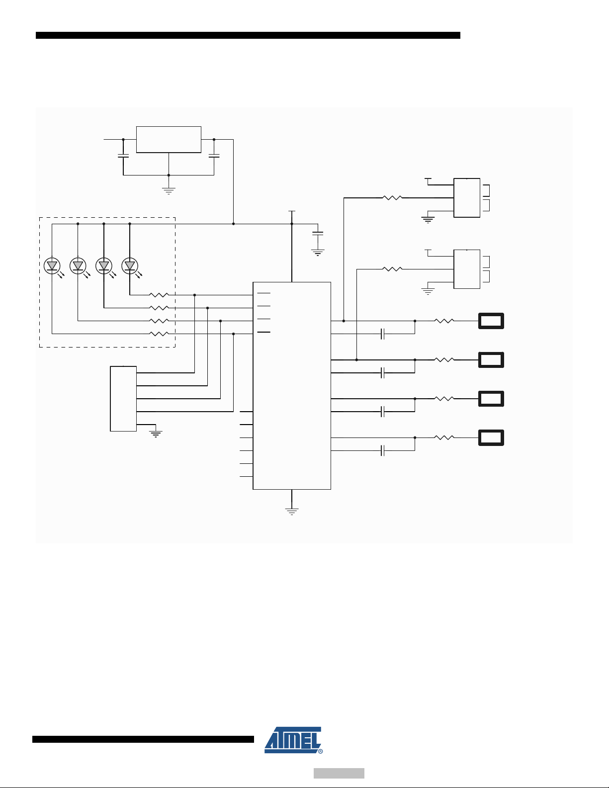
Atmel QTouch AT42QT1040 Instruction Manual

Features
•Number of Keys:
–Upto4
•Discrete Outputs:
– 4 discrete outputs indicating individual key touch
•Technology:
– Patented spread-spectrum charge-transfer (direct mode)
•Electrode Design:
– Simple self-capacitance style (refer to the Touch Sensors Design Guide)
•Electrode Materials:
– Etched copper, silver, carbon, Indium Tin Oxide (ITO)
•Electrode Substrates:
– PCB, FPCB, plastic films, glass
•Panel Materials:
– Plastic, glass, composites, painted surfaces (low particle density metallic paints
possible)
•Panel Thickness:
– Up to 10 mm glass, 5 mm plastic (electrode size dependent)
•Key Sensitivity:
– Fixed key threshold, sensitivity adjusted via sample capacitor value
•Adjacent Key Suppression™
– Patented Adjacent Key Suppression™(AKS™) technology to enable accurate key
detection
•Interface:
– Pin-per-key outputs, plus debug mode to observe sensor signals
•Moisture Tolerance:
–Good
•Power:
– 1.8V ~ 5.5V
•Package:
– 20-pin 3 x 3 mm VQFN RoHS compliant
•Signal Processing:
– Self-calibration, auto drift compensation, noise filtering, Adjacent Key
Suppression technology
•Applications:
– Mobile, consumer, white goods, toys, kiosks, POS, and so on
QTouch™4-key
Sensor IC
AT42QT1040
9524B–AT42–04/09
Downloaded From Oneyac.com

2
9524B–AT42–04/09
AT42QT1040
1. Pinout and Schematic
1.1 Pinout Configuration
I/O CMOS input and output OD CMOS open drain output P Ground or power
Table 1-1. Pin Listing
Pin Name Type Function Notes If Unused...
1 SNS2 I/O Sense pin To Cs2 Leave open
2 SNSK1 I/O Sense pin and
option detect To Cs1 and option resistor + key Connect to option resistor*
3 SNS1 I/O Sense pin To Cs1 Leave open
4 SNSK0 I/O Sense pin and
option detect To Cs0 and option resistor + key Connect to option resistor*
5 SNS0 I/O Sense pin To Cs0 Leave open
6N/C– – –
7N/C– – –
8 Vss P Supply ground –
9 Vdd P Power –
10 N/C – – –
11 OUT0 OD Out 0 Alternative function: Debug CLK Leave open
12 OUT1 OD Out 1 Alternative function: Debug DATA Leave open
13 OUT3 OD Out 3 Leave open
14 OUT2 OD Out 2 Leave open
15 SNSK3 I/O Sense pin To Cs3 + key Leave open
16 SNS3 I/O Sense pin To Cs3 Leave open
17 N/C – – –
18 N/C – – –
19 N/C – – –
20 SNSK2 I/O Sense pin To Cs2 + key Leave open
* Option resistor should always be fitted even if channel is unused and Cs capacitor is not fixed.
N/C
N/C
VSS
VDD
N/C
SNS2
SNSK1
SNS1
SNSK0
SNS0 OUT0
OUT1
1
2
3
4
511
12
13
14
15
20 19 18 17 16
67810
9
QT1040
OUT3
OUT2
SNSK3
SNS3
N/C
SNSK2
N/C
N/C
Downloaded From Oneyac.com

3
9524B–AT42–04/09
AT42QT1040
1.2 Schematic
Figure 1-1. Typical Circuit
Suggested regulator manufacturers:
• Torex (XC6215 series)
• Seiko (S817 series)
• BCDSemi (AP2121 series)
Re Figure 1-1 check the following sections for component values:
•Section3.1onpage6: Cs capacitors (Cs0 – Cs3)
•Section3.5onpage7: Voltage levels
•Section3.3onpage6: LED traces
SLOW
FAST
OFF
LED3
LED2
LED0
LED1
VDD
VDD
2
1
3
J2
VDD
2
1
3
J1
ON
22
55
44
33
11
J3
VDD 9
VSS
8
N/C
19
N/C
10
OUT2
14
SNSK3 15
SNSK2 20
SNSK1 2
SNSK0 4
N/C
18
N/C
7
N/C
17
OUT1
12
OUT0
11
SNS3 16
SNS1 3
N/C
6
OUT3
13 SNS0 5
SNS2 1
SPEED SELECT
AKS SELECT
NOTES:
1) The central pad on the underside of the VQFN chip is a Vss pin and should be connected
to ground. Do not put any other tracks underneath the body of the chip.
2) It is important to place all Cs and Rs components physically near to the chip.
Add a 100 nF capacitor close to pin 9.
QT1040
Creg Creg
VREG
Follow regulator manufacturer's
recommended values for input
and output bypass capacitors (Creg).
Key0
Key1
Key2
Key3
VUNREG
GND
Cs0
Cs1
Cs2
Cs3
RL0
RL1
RL2
RL3
RAKS
RFS
Rs0
Rs1
Rs2
Rs3
Example use of output pins
Downloaded From Oneyac.com

4
9524B–AT42–04/09
AT42QT1040
2. Overview of the AT42QT1040
2.1 Introduction
The AT42QT1040 (QT1040) is a digital burst mode charge-transfer (QT™) capacitive sensor
driver designed for touch-key applications. The device can sense from one to four keys; one to
three keys can be disabled by not installing their respective sense capacitors. Any of the four
channels can be disabled in this way.
The device includes all signal processing functions necessary to provide stable sensing under a
wide variety of changing conditions, and the outputs are fully debounced. Only a few external
parts are required for operation.
The QT1040 modulates its bursts in a spread-spectrum fashion in order to heavily suppress the
effects of external noise, and to suppress RF emissions.
2.2 Signal Processing
2.2.1 Detect Threshold
The internal signal threshold level is fixed at 10 counts of change with respect to the internal
reference level. This in turn adjusts itself slowly in accordance with the drift compensation
mechanism. See Section 3.1 on page 6 for details on how to adjust each key’s sensitivity.
When going out of detect there is a hysteresis element to the detection. The signal threshold
must drop below 8 counts of change with respect to the internal reference level to register as un-
touched.
2.2.2 Detection Integrator
The device features a detection integration mechanism, which acts to confirm a detection in a
robust fashion. A per-key counter is incremented each time the key has exceeded its threshold,
and a key is only finally declared to be touched when this counter reaches a fixed limit of 5. In
other words, the device has to exceed its threshold, and stay there for 5 acquisitions in
succession without going below the threshold level, before the key is declared to be touched.
2.2.3 Burst Length Limitations
Burst length is the number of times the charge transfer process is performed on a given channel;
that is, the number of pulses it takes to measure the key’s capacitance.
The maximum burst length is 2048 pulses. The recommended design is to use a capacitor that
gives a signal of <1000 pulses. Longer bursts take more time and use more power.
Note that the keys are independent of each other. It is therefore possible, for example, to have a
signal of 100 on one key and a signal of 1000 on another.
Refer to Application Note QTAN0002, Secrets of a Successful QTouch™ Design (downloadable
from the Atmel®website), for more information on using a scope to measure the pulses and
hence determine the burst length. Refer also to the Touch Sensors Design Guide.
2.2.4 Adjacent Key Suppression Technology
The device includes Atmel’s patented Adjacent Key Suppression (AKS) technology, to allow the
use of tightly spaced keys on a keypad with no loss of selectability by the user.
There is one global AKS group, implemented so that only one key in the group may be reported
as being touched at any one time.
Downloaded From Oneyac.com

5
9524B–AT42–04/09
AT42QT1040
The use of AKS is selected by connecting a 1 Mresisitor between Vdd and the SNSK0 pin
(see Section 4.1 on page 8 for more information). When AKS is disabled, any combinations of
keys can enter detect.
2.2.5 Auto Drift Compensation
Signal drift can occur because of changes in Cx and Cs over time. It is crucial that drift be
compensated for, otherwise false detections, non-detections, and sensitivity shifts will follow.
Drift compensation is performed by making the reference level track the raw signal at a slow
rate, but only while there is no detection in effect. The rate of adjustment must be performed
slowly otherwise legitimate detections could be ignored.
Once an object is sensed and a key is in detect, the drift compensation mechanism ceases,
since the signal is legitimately high and should not therefore cause the reference level to
change.
The QT1040's drift compensation is “asymmetric”: the reference level drift-compensates in one
direction faster than it does in the other. Specifically, it compensates faster for decreasing
(towards touch) signals than for increasing (away from touch) signals. The reason for this
difference in compensation rates is that increasing signals should not be compensated for
quickly, since a nearby finger could be compensated for partially or entirely before even
approaching the sense electrode. However, decreasing signals need to be compensated for
more quickly. For example, an obstruction over the sense pad (for which the sensor has already
made full allowance) could suddenly be removed, leaving the sensor with an artificially elevated
reference level and thus become insensitive to touch. In this latter case, the sensor will
compensate for the object's removal very quickly, usually in only a few seconds.
Negative drift (that is, towards touch) occurs at a rate of ~3 seconds, while positive drift occurs at
a rate of ~1 second.
Drifting only occurs when no keys are in detect state.
2.2.6 Response Time
The QT1040's response time is highly dependent on run mode and burst length, which in turn is
dependent on Cs and Cx. With increasing Cs, response time slows, while increasing levels of Cx
reduce response time. The response time will also be slower in slow mode due to a longer time
between burst measurements. This mode offers an increased detection latency in favor of
reduced average current consumption.
2.2.7 Spread Spectrum
The QT1040 modulates its internal oscillator by ±7.5 percent during the measurement burst.
This spreads the generated noise over a wider band reducing emission levels. This also reduces
susceptibility since there is no longer a single fundamental burst frequency.
2.2.8 Max On-duration
If an object or material obstructs the sense pad, the signal may rise enough to create a
detection, preventing further operation. To prevent this, the sensor includes a timer known as
the Max On-duration feature which monitors detections. If a detection exceeds the timer setting,
the sensor performs an automatic recalibration. Max On-duration is set to ~30s.
Downloaded From Oneyac.com

6
9524B–AT42–04/09
AT42QT1040
3. Wiring and Parts
3.1 Cs Sample Capacitors
Cs0 – Cs3 are the charge sensing sample capacitors; normally they are identical in nominal
value. The optimal Cs values depend on the corresponding keys electrode design, the thickness
of the panel and its dielectric constant. Thicker panels require larger values of Cs. Values can be
in the range 2.2 nF (for faster operation) to 22 nF (for best sensitivity); typical values are 4.7 nF
to 10 nF.
The value of Cs should be chosen such that a light touch on a key mounted in a production unit
or a prototype panel causes a reliable detection. The chosen Cs value should never be so large
that the key signals exceed ~1000, as reported by the chip in the debug data.
The Cs capacitors must be X7R or PPS film type, for stability. For consistent sensitivity, they
should have a 10 percent tolerance. Twenty percent tolerance may cause small differences in
sensitivity from key to key and unit to unit. If a key is not used, the Cs capacitor may be omitted.
3.2 Rs Resistors
The series resistors Rs0 – Rs3 are inline with the electrode connections (close to the QT1040
chip) and are used to limit electrostatic discharge (ESD) currents and to suppress radio
frequency (RF) interference. A typical value is 4.7 k, but up to 20 kcan be used if it is found
to be of benefit.
Although these resistors may be omitted, the device may become susceptible to external noise
or radio frequency interference (RFI). For details on how to select these resistors refer to
Application Note QTAN0002, Secrets of a Successful QTouch™Design, and the Touch Sensors
Design Guide, both downloadable from the Touch Technology area of Atmel’s website,
www.atmel.com.
3.3 LED Traces and Other Switching Signals
For advice on LEDs and nearby traces, refer to Application Note QTAN0002, Secrets of a
Successful QTouch™Design, and the Touch Sensors Design Guide, both downloadable from
the Touch Technology area of Atmel’s website, www.atmel.com.
3.4 PCB Cleanliness
Modern no-clean flux is generally compatible with capacitive sensing circuits.
If a PCB is reworked in any way, clean it thoroughly to remove all traces of the flux residue
around the capacitive sensor components. Dry it thoroughly before any further testing is
conducted.
CAUTION: If a PCB is reworked in any way, it is almost guaranteed that the behavior
of the no-clean flux will change. This can mean that the flux changes from an inert
material to one that can absorb moisture and dramatically affect capacitive
measurements due to additional leakage currents. If so, the circuit can become
erratic and exhibit poor environmental stability.
Downloaded From Oneyac.com

7
9524B–AT42–04/09
AT42QT1040
3.5 Power Supply
See Section5.2onpage13for the power supply range. If the power supply fluctuates slowly
with temperature, the device tracks and compensates for these changes automatically with only
minor changes in sensitivity. If the supply voltage drifts or shifts quickly, the drift compensation
mechanism is not able to keep up, causing sensitivity anomalies or false detections.
The usual power supply considerations with QT parts apply to the device. The power should be
clean and come from a separate regulator if possible. However, this device is designed to
minimize the effects of unstable power, and except in extreme conditions should not require a
separate Low Dropout (LDO) regulator.
See under Figure 1.2 on page 3 for suggested regulator manufacturers.
It is assumed that a larger bypass capacitor (for example, 1 µF) is somewhere else in the power
circuit; for example, near the regulator.
To assist with transient regulator stability problems, the QT1040 waits 500 µs any time it wakes
up from a sleep state (that is, in Sleep mode) before acquiring, to allow Vdd to fully stabilize.
3.6 VQFN Package Restrictions
The central pad on the underside of the VQFN chip should be connected to ground. Do not run
any tracks underneath the body of the chip, only ground. Figure 3-1 shows an example of
good/bad tracking.
Figure 3-1. Examples of Good and Bad Tracking
Caution: A regulator IC shared with other logic can result in erratic operation and is
not advised.
A single ceramic 0.1 µF bypass capacitor, with short traces, should be placed very
close to the power pins of the IC. Failure to do so can result in device oscillation,
high current consumption, erratic operation, and so on.
Example of GOOD tracking Example of BAD tracking
Downloaded From Oneyac.com

8
9524B–AT42–04/09
AT42QT1040
4. Detailed Operations
4.1 Adjacent Key Suppression
The use of AKS is selected by the connection of a 1 Mresistor (RAKS resistor) between the
SNSK0 pin and either Vdd (AKS mode on) or Vss (AKS mode off).
Note: Changing the RAKS option will affect the sensitivity of the particular key. Always check
that the sensitivity is suitable after a change. Retune Cs0 if necessary.
4.2 Discrete Outputs
There are four discrete outputs (channels 0 to 3), located on pins OUT0 to OUT3. An output pin
goes active when the corresponding key is touched. The outputs are open-drain type and are
active-low.
On the OUT2 pin there is a ~500 ns low pulse occuring approximately 20 ms after a power-
up/reset (see Figure 4-1 for an example oscilloscope trace of this pulse at two zoom levels). This
pulse may need to be considered from the system design perspective.
The discrete outputs have sufficient current sinking capability to directly drive LEDs. Try to limit
the sink current to less than 5 mA per output and be cautious if connecting LEDs to a power
supply other than Vdd; if the LED supply is higher than Vdd it may cause erratic behavior of the
QT1040 and “back-power” the QT1040 through its I/O pins.
Table 4-1. RAKS Resistor
RAKS Connected To... Mode
Vdd AKS on
Vss AKS off
The RAKS resistor should always be connected to either Vdd or Vss and should not be
changed during operation of the device.
Downloaded From Oneyac.com

9
9524B–AT42–04/09
AT42QT1040
Figure 4-1. ~500 ns Pulse On OUT2 Pin
4.3 Speed Selection
Speed selection is determined by a 1 Mresistor (RFS resistor) connected between SNSK1
and either Vdd (Fast Mode) or Vss (Slow Mode).
In Fast Mode, the device sleeps for 16 ms between burst acquisitions. In Slow Mode, the device
sleeps for 64 ms between acquisitions. Hence, Slow Mode conserves more power but results in
slightly less responsiveness.
Note: The RFS resistor should always be connected to either Vdd or Vss and not changed
during operation of the device. Changing the RFS option will affect the sensitivity of the
particular key. Always check that the sensitivity is suitable after a change. Retune Cs1 if
necessary.
Pulse on OUT2
SNS0K
OUT2
SNS0K
OUT2
~20 ms
Power-on/
Reset
Table 4-2. RFS Resistor
RFS Connected To... Mode
Vdd Fast mode
Vss Slow mode
Downloaded From Oneyac.com

10
9524B–AT42–04/09
AT42QT1040
4.4 Calibration
Calibration is the process by which the sensor chip assesses the background capacitance on
each channel. During calibration, a number of samples are taken in quick succession to get a
baseline for the channel’s reference value.
Calibration takes place ~50 ms after power is applied to the device. Calibration also occurs if the
Max On-duration is exceeded or a positive re-calibration occurs.
4.5 Debug Mode
An added feature to this device is a debug option whereby internal parameters from the IC can
be clocked out and monitored externally.
Debug mode is entered by shorting the CS3 capacitor (SNSK3 and SNS3 pins) on power-up
and removing the short within 5 seconds.
Note: If the short is not removed within 5 seconds, debug mode is still entered, but with
Channel 3 unusable until a re-calibration occurs. Note that as Channel 3 will show up as
being in detect, a recalibration will occur after Max On-duration (~30 seconds).
Debug CLK pin (OUT0) and Debug Data pin (OUT1) float while debug data is not being output
and are driven outputs once debug output starts (that is, not open drain).
The serial data is clocked out at a rate of ~200 kHz, MSB first, as in Table 4-3.
Table 4-3. Serial Data Output
Byte Purpose Notes
0 Frame Number Framing index number 0-255
1ChipVersion Upper nibble: major revision
Lower nibble: minor revision
2 Reference 0 Low Byte Unsigned 16-bit integer
3 Reference 0 High Byte
4 Reference 1 Low Byte Unsigned 16-bit integer
5 Reference 1 High Byte
6 Reference 2 Low Byte Unsigned 16-bit integer
7 Reference 2 High Byte
8 Reference 3 Low Byte Unsigned 16-bit integer
9 Reference 3 High Byte
10 Signal 0 Low Byte Unsigned 16-bit integer
11 Signal 0 High Byte
12 Signal 1 Low Byte Unsigned 16-bit integer
13 Signal 1 High Byte
14 Signal 2 Low Byte Unsigned 16-bit integer
15 Signal 2 High Byte
16 Signal 3 Low Byte Unsigned 16-bit integer
17 Signal 3 High Byte
Downloaded From Oneyac.com

11
9524B–AT42–04/09
AT42QT1040
Bit 7: This bit is set during calibration
Bits 4 – 6: Contains the number of keys active
Bits 0 – 3: Show the touch status of the corresponding keys
Figure 4-2 to Figure 4-5 show the usefulness of the debug data out feature. Channels can be
monitored and tweaked to the specific application with great accuracy.
Figure 4-2. Byte Clocked Out (~5 µs Period)
18 Delta 0 Low Byte Signed 16-bit integer
19 Delta 0 High Byte
20 Delta 1 Low Byte Signed 16-bit integer
21 Delta 1 High Byte
22 Delta 2 Low Byte Signed 16-bit integer
23 Delta 2 High Byte
24 Delta 3 Low Byte Signed 16-bit integer
25 Delta 3 High Byte
26 Flags Various operational flags
Unsigned bytes
27 Flags2
28 Status Byte Unsigned byte. See Table 4-4
29 Frame Number Repeat of framing index number in
byte 0
Table 4-4. Status Byte (Byte 28)
Bit 7 Bit 6 Bit 5 Bit 4 Bit 3 Bit 2 Bit 1 Bit 0
CAL Number of Keys (2-4) Key 3 Key 2 Key 1 Key 0
Table 4-3. Serial Data Output (Continued)
Byte Purpose Notes
Downloaded From Oneyac.com

13
9524B–AT42–04/09
AT42QT1040
5. Specifications
5.1 Absolute Maximum Specifications
5.2 Recommended Operating Conditions
5.3 DC Specifications
Vdd -0.5 to +6.0V
Max continuous pin current, any control or drive pin ±10 mA
Voltage forced onto any pin -0.5V to (Vdd + 0.5) Volts
CAUTION: Stresses beyond those listed under Absolute Maximum Specifications may cause permanent damage to the
device. This is a stress rating only and functional operation of the device at these or other conditions beyond those
indicated in the operational sections of this specification is not implied. Exposure to absolute maximum specification
conditions for extended periods may affect device reliability
Operating temperature -40°C to +85°C
Storage temperature -55°C to +125°C
Vdd 1.8V to 5.5V
Supply ripple + noise ±20 mV maximum
Cx capacitance per key 2 to 20 pF
Vdd = 5.0V, Cs = 4.7 nF, Ta = recommended range, unless otherwise noted
Parameter Description Min Typ Max Units Notes
Vil Low input logic level -0.5V – 0.3V V
Vih High input logic level 0.6 Vdd Vdd Vdd + 0.5V V
Vol Low output voltage 0 – 0.7 V 10 mA sink current
Voh High output voltage 0.8 Vdd – Vdd V 10 mA source current
Iil Input leakage current – <0.05 1 µA
Rrst Internal RST pull-up resistor 20 – 50 k
Downloaded From Oneyac.com

14
9524B–AT42–04/09
AT42QT1040
5.4 Timing Specifications
5.5 Power Consumption
Parameter Description Min Typ Max Units Notes
TBS Burst duration – 3.5 – ms Cx = 5 pF, Cs = 18 nF
Fc Burst center frequency – 119 kHz
Fm Burst modulation, percentage -7.5 – +7.5 %
TPW Burst pulse width – 2 – µs
Vdd (V) AKS Mode (RAKS) Speed (RFS) Power Consumption (µA)
1.8 Off Slow 31
Off Fast 104
On Slow 36
On Fast 114
3.3 Off Slow 100
Off Fast 340
On Slow 117
On Fast 380
5.0 Off Slow 215
Off Fast 710
On Slow 245
On Fast 800
Downloaded From Oneyac.com

15
9524B–AT42–04/09
AT42QT1040
5.6 Mechanical Dimensions
TITLE DRAWING NO.GPC REV.
Package DrawingContact:
packagedrawings@atmel.com 20M2ZFC B
20M2, 20-pad,3 x 3 x 0.85 mm Body, Lead Pitch 0.45 mm,
1.55 x 1.55 mm Exposed Pad, Thermally Enhanced
Plastic Very Thin Quad Flat No Lead Package (VQFN)
10/24/08
15
14
13
12
11
1
2
3
4
5
16 17 1819 20
10 9 87 6
D2
E2
e
b
K
L
Pin #1 Chamfer
(C 0.3)
D
E SIDE VIEW
A1
y
Pin 1 ID
BOTTOM VIEW
TOP VIEW
A1
A
C
C0.18(8X)
0.3Ref (4x)
COMMON DIMENSIONS
(Unit of Measure = mm)
SYMBOL MIN NOM MAX NOTE
A 0.75 0.80 0.85
A1 0.00 0.02 0.05
b0.17 0.22 0.27
C 0.152
D 2.90 3.00 3.10
D2 1.40 1.55 1.70
E 2.90 3.00 3.10
E2 1.40 1.55 1.70
e –0.45 –
L 0.35 0.40 0.45
K 0.20 ––
y 0.00 –0.08
Downloaded From Oneyac.com

16
9524B–AT42–04/09
AT42QT1040
5.7 Marking
Either of the following two markings may be used:
Program Week Code Number 1-52 Where:
A = 1 B = 2 ... Z = 26
then using the underscore A = 27...Z = 52
140
R1
Pin1 ID
Code Revision:
1.0 Released
Abbreviation of
PartNumber:
AT42QT1040
140
R1X
Pin1 ID
Code Revision:
R1 = 1.0 Released
Abbreviation of
PartNumber:
AT42QT
1
0
40
Traceability Code
(Y = last digit of year; for example, 9 = 2009, 0 = 2010, etc
ZZ = assembly trace code)
Assembly
Location Code
YZZ
Downloaded From Oneyac.com

17
9524B–AT42–04/09
AT42QT1040
5.8 Part Number
5.9 Moisture Sensitivity Level (MSL)
Revision History
Part Number Description
AT42QT1040-MMH 20-pin 3 x 3 mm VQFN RoHS compliant
MSL Rating Peak Body Temperature Specifications
MSL1 260oC IPC/JEDEC J-STD-020
Revision No. History
Revision A – March 2009 Initial release for chip revision 1.0
Revision B – April 2009 Update to pin listing in Table 1-1
Downloaded From Oneyac.com

9524B–AT42–04/09
Headquarters International
Atmel Corporation
2325 Orchard Parkway
San Jose, CA 95131
USA
Tel: 1(408) 441-0311
Fax: 1(408) 487-2600
Atmel Asia
Unit 01-05 & 16, 19/F
BEA Tower, Millennium City 5
418 Kwun Tong Road
Kwun Tong
Kowloon
Hong Kong
Tel: (852) 2245-6100
Fax: (852) 2722-1369
Atmel Europe
Le Krebs
8, Rue Jean-Pierre Timbaud
BP 309
78054 Saint-Quentin-en-
Yvelines Cedex
France
Tel: (33) 1-30-60-70-00
Fax: (33) 1-30-60-71-11
Atmel Japan
9F, Tonetsu Shinkawa Bldg.
1-24-8 Shinkawa
Chuo-ku, Tokyo 104-0033
Japan
Tel: (81) 3-3523-3551
Fax: (81) 3-3523-7581
Touch Technology Division
1 Mitchell Point
Ensign Way
Hamble
Southampton
Hampshire SO31 4RF
United Kingdom
Tel: (44) 23-8056-5600
Fax: (44) 23-8045-3939
Product Contact
Web Site
www.atmel.com
Technical Support
Sales Contact
www.atmel.com/contacts
Literature Requests
www.atmel.com/literature
Disclaimer: The information in this document is provided in connection with Atmel products. No license, express or implied, by estoppel or otherwise, to any
intellectual property right is granted by this document or in connection with the sale of Atmel products. EXCEPT AS SET FORTH IN ATMEL’S TERMS AND
CONDITIONS OF SALE LOCATED ON ATMEL’S WEB SITE, ATMEL ASSUMES NO LIABILITY WHATSOEVER AND DISCLAIMS ANY EXPRESS, IMPLIED OR
STATUTORY WARRANTY RELATING TO ITS PRODUCTS INCLUDING, BUT NOT LIMITED TO, THE IMPLIED WARRANTY OF MERCHANTABILITY, FITNESS
FOR A PARTICULAR PURPOSE, OR NON-INFRINGEMENT. IN NO EVENT SHALL ATMEL BE LIABLE FOR ANY DIRECT, INDIRECT, CONSEQUENTIAL,
PUNITIVE, SPECIAL OR INCIDENTAL DAMAGES (INCLUDING, WITHOUT LIMITATION, DAMAGES FOR LOSS OF PROFITS, BUSINESS INTERRUPTION, OR
LOSS OF INFORMATION) ARISING OUT OF THE USE OR INABILITY TO USE THIS DOCUMENT, EVEN IF ATMEL HAS BEEN ADVISED OF THE POSSIBILITY
OF SUCH DAMAGES. Atmel makes no representations or warranties with respect to the accuracy or completeness of the contents of this document and reserves the
right to make changes to specifications and product descriptions at any time without notice. Atmel does not make any commitment to update the information
contained herein. Unless specifically provided otherwise, Atmel products are not suitable for, and shall not be used in, automotive applications. Atmel’s products are
not intended, authorized, or warranted for use as components in applications intended to support or sustain life.
© 2009 Atmel Corporation. All rights reserved. Atmel®, Atmel logo and combinations thereof, and others are registered trademarks, Adjacent
Key Suppression™, AKS™, QT™, QTouch™, and others are trademarks of Atmel Corporation or its subsidiaries. Other terms and product names
may be registered trademarks or trademarks of others.
Downloaded From Oneyac.com
Table of contents
Other Atmel Accessories manuals

Atmel
Atmel FingerChip AT77UR200 User manual

Atmel
Atmel ATA6264 User manual

Atmel
Atmel QTAN0087 Installation and operating instructions

Atmel
Atmel ATA5577 User manual

Atmel
Atmel ATR4262M1 User manual

Atmel
Atmel QTouch AT42QT2120 User manual

Atmel
Atmel FingerChip AT77UR200 User manual

Atmel
Atmel CryptoRF AT88SC0104CRF User manual

Atmel
Atmel ATA5283 User manual

Atmel
Atmel AT88RF020 User manual