Atmel AT91 Series User manual
Other Atmel Microcontroller manuals
Atmel
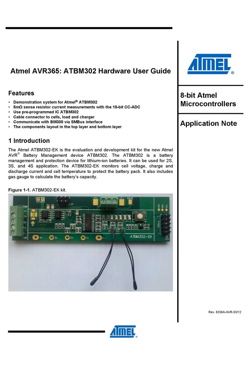
Atmel AVR365 User manual
Atmel
Atmel ATmega128A-STK600 Installation and operating instructions
Atmel
Atmel AT89STK-03 Installation manual
Atmel
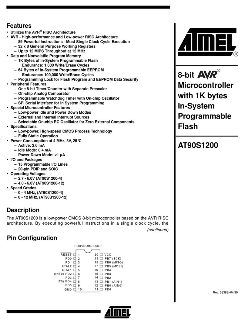
Atmel AVR4901 Installation and operating instructions
Atmel
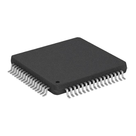
Atmel AT90S1200 User manual
Atmel
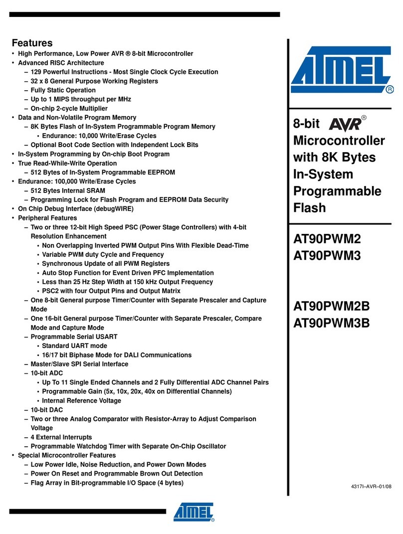
Atmel AVR AT90CAN32 User manual
Atmel
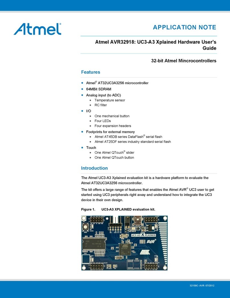
Atmel AT90PWM2 User manual
Atmel
Atmel AVR32918 User manual
Atmel
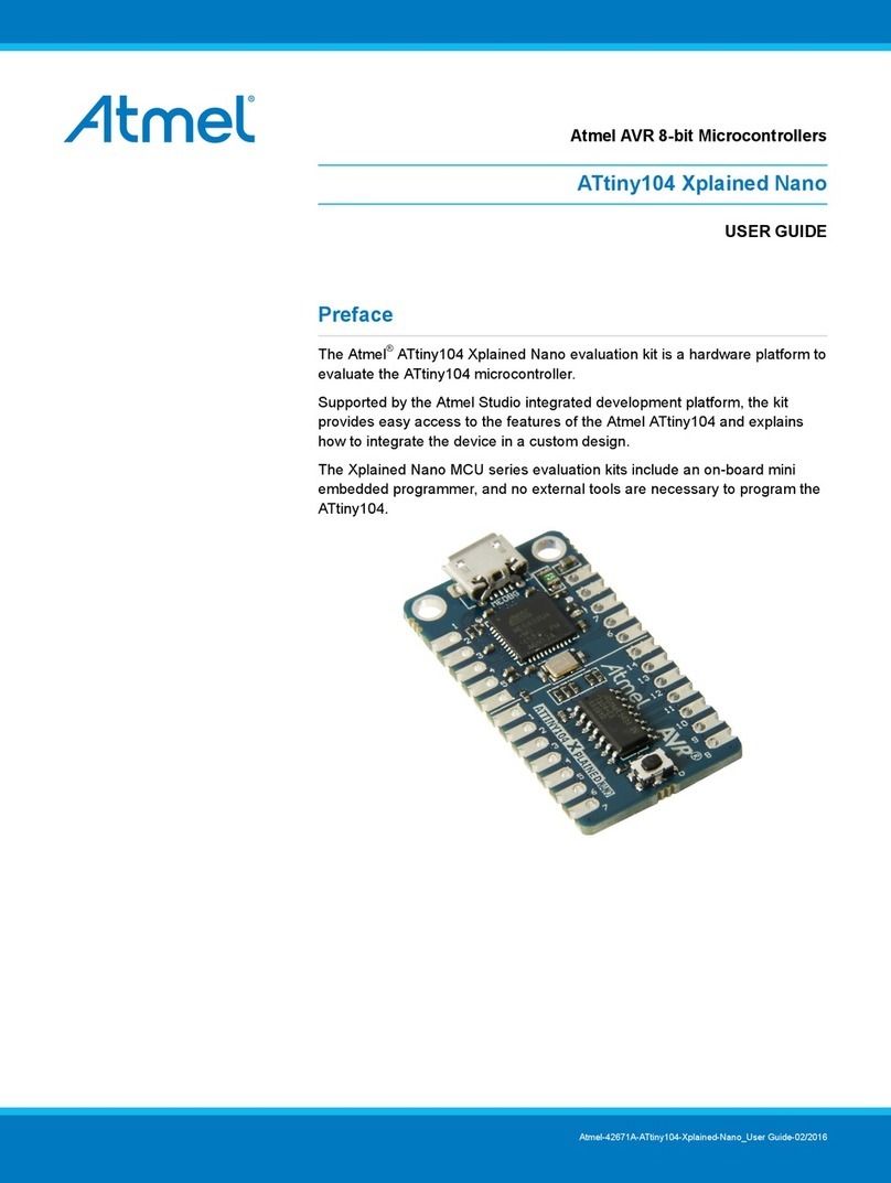
Atmel ATtiny104 Xplained Nano User manual
Atmel
Atmel ATF15 DK2 Series User manual
Atmel
Atmel AVR042 Installation and operating instructions
Atmel
Atmel C51 Installation and operating instructions
Atmel
Atmel AVR ATtiny22 Instruction Manual
Atmel
Atmel ATmega48PV User manual
Atmel
Atmel AT97SC3205T-SDK2 User manual
Atmel
Atmel 80C51 Installation and operating instructions
Atmel
Atmel 80C51 Installation and operating instructions
Atmel
Atmel ATAB5749 Installation and operating instructions

Atmel
Atmel QT600 User manual
Atmel
Atmel AT01607 Installation and operating instructions
Popular Microcontroller manuals by other brands
AMS
AMS AS7261 Demo Kit user guide

Novatek
Novatek NT6861 manual
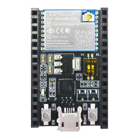
Espressif Systems
Espressif Systems ESP8266 SDK AT Instruction Set
Nuvoton
Nuvoton ISD61S00 ChipCorder Design guide
STMicrolectronics
STMicrolectronics ST7 Assembler Linker user manual
Texas Instruments
Texas Instruments Chipcon CC2420DK user manual

Texas Instruments
Texas Instruments TMS320F2837 D Series Workshop Guide and Lab Manual
CYPRES
CYPRES CY14NVSRAMKIT-001 user guide
Texas Instruments
Texas Instruments INA-DUAL-2AMP-EVM user guide
Espressif Systems
Espressif Systems ESP8266EX Programming guide
Abov
Abov AC33M8128L user manual
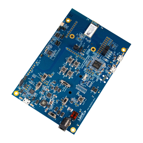
Laird
Laird BL654PA user guide
