BBK DL385DC User manual

SERVICE MANUAL
DL385DC

CONTENTS
1. SAFETY PRECAUTIONS 1
2. PREVENTION OF ELECTRO STATIC DISCHARGE(ESD)TO ELECTROSTATICALLY
SENSITIVE(ES)DEVICES 1
4. PREVERTION OF STATIC ELECTRICITY DISCHARGE 4
5.ELECTRICALCONFIRMATION5
5.1VIDEOOUTPUT(LUMINANCESIGNAL)CONFIRMATION5
5.2VIDEOOUTPUT(CHROMINANCESIGNAL)CONFIRMATION6
6.MPEGBOARDCHECKWAVEFORM7
8.SCHEMATIC&PCBWIRINGDIAGRAM
17
9.SPAREPARTSLIST33
7.2MT13898
7.3HY29LV160 11
7.4HY57V641620HG
14
3. CONTROL BUTTON LOCATIONS AND EXPLANATIONS 2

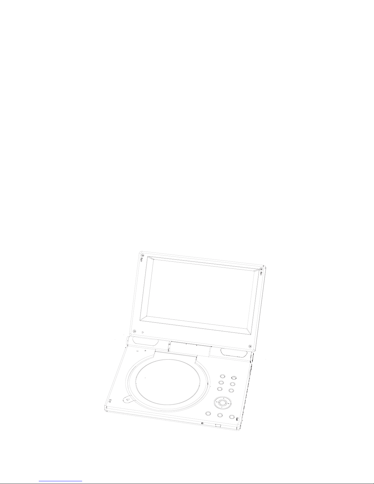
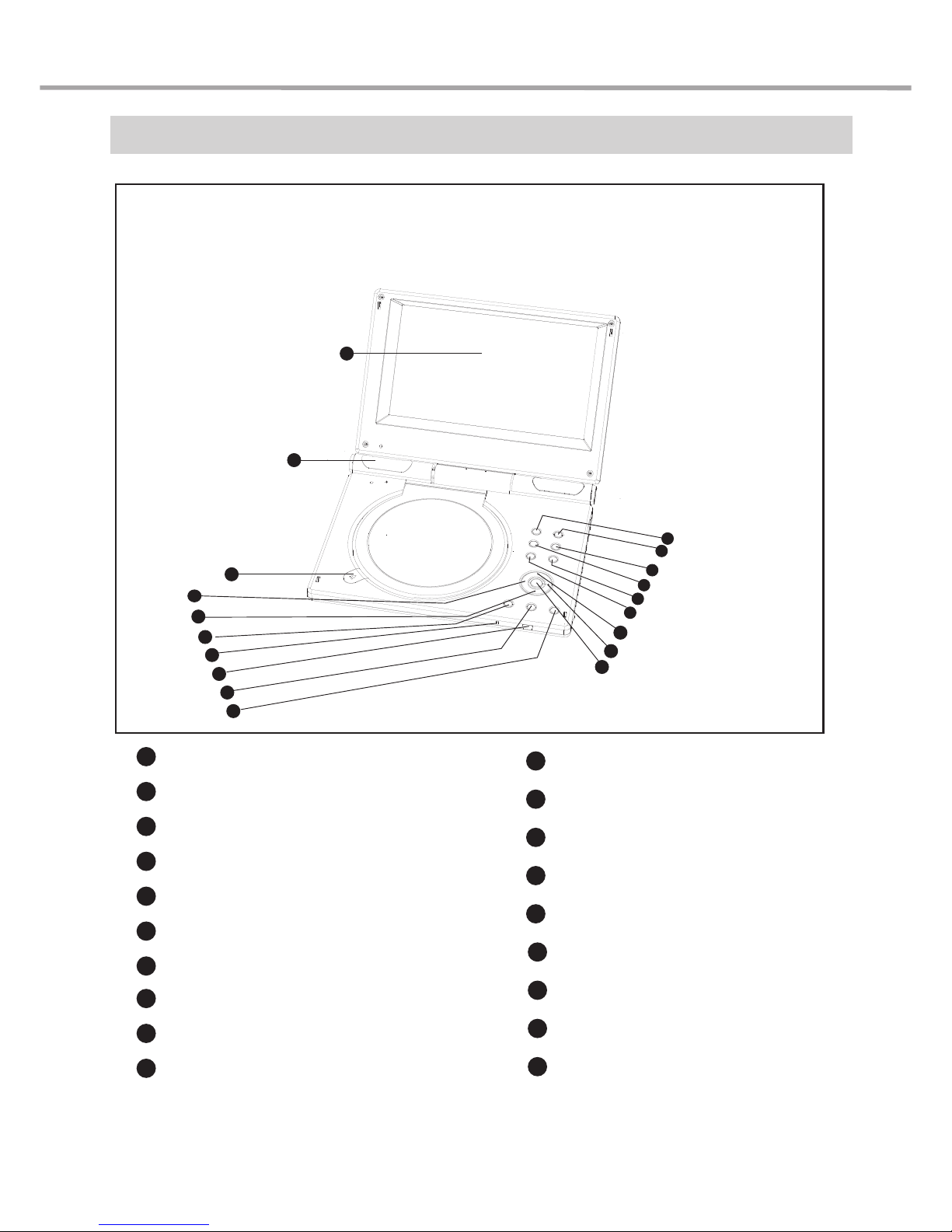
1.1 GENERAL GUIDELINES
1. When servicing, observe the original lead dress. if a short circuit is found, replace all parts which have
been overheated or damaged by the short circuit.
2. After servicing, see to it that all the protective devices such as insulation barrier, insulation papers
shields are properly installed.
3. After servicing, make the following leakage current checks to prevent the customer from being exposed
to shock hazards.
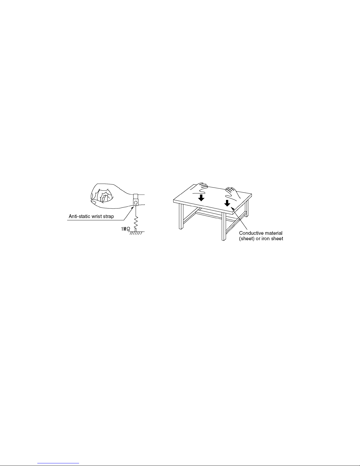
Some semiconductor(solid state)devices can be damaged easily by static electricity. Such components
commonly are called Electrostatically Sensitive(ES)Devices. Examples of typical ES devices are integrated
circuits and some field-effect transistors and semiconductor chip components. The following techniques
should be used to help reduce the incidence of component damage caused by electro static discharge(ESD).
1. Immediately before handling any semiconductor component or semiconductor-equipped assembly, drain
off any ESD on your body by touching a known earth ground. Alternatively, obtain and wear a commercially
availabel discharging ESD wrist strap, which should be removed for potential shock reasons prior to
applying power to the unit under test.
2. After removing an electrical assembly equipped with ES devices,place the assembly on a conductive
surface such as alminum foil, to prevent electrostatic charge buildup or exposure of the assembly.
3. Use only a grounded-tip soldering iron to solder or unsolder ES devices.
4. Use only an anti-static solder removal device. Some solder removal devices not classified as anti-static
(ESD protected)can generate electrical charge sufficient to damage ES devices.
5. Do not use freon-propelled chemicals. These can generate electrical charges sufficient to damage ES
devices.
6. Do not remove a replacement ES device from its protective package until immediately before you are
ready to install it.(Most replacement ES devices are packaged with leads electrically shorted together by
conductive foam, alminum foil or comparable conductive material).
7. Immediately before removing the protective material from the leads of a replacement ES device, touch
the protective material to the chassis or circuit assembly into which the device will be installed.
Caution
Be sure no power is applied to the chassis or circuit, and observe all other safety precautions.
8. Minimize bodily motions when handling unpackaged replacement ES devices. (Otherwise harmless motion
such as the brushing together of your clothes fabric or the lifting of your foot from a carpeted floor can
generate static electricity(ESD).
notice (1885x323x2 tiff)

Control Button Locations and Explanations
1
Color TFT LCD
2
Speakers
3
4
LEFT direction arrow
5
6
9
IR sensor
7
Power indicator
8
PREV Button
10
PLAY button / PAUSE button
11
RIGHT direction arrow
12
UP direction arrow
15
13
14
2
1
3
514
17
16
15
18
19
7
9
6
8
10
11
1134
12
OPEN/CLOSE button
DVD/READER button
DOWN direction arrow
17
P/N button
18
MENU Button
19
SETUP Button
NEXT Button
STOP button
4
Panel Button
16
DVD/AUXIN Button

3
Remote Control Illustration
6
3
2
5
7
8
9
12
11
13
14
16
33
22
20
18
21
19
23
24
28
27
25
26
15
17
4
31
32
30
29
10
35
34
Switch new user interface.
BROWSER
18
DVD/READER Button
Change the audio language or
audio channel.
AUDIO Button
2
Play from the desired location.
GOTO button
3
Zoom in /out the displayed frame.
ZOOM Button
4
Fast forward play.
FWD Button
14
Change camera angles, MP3/JPEG
playback modes switch.
ANGLE Button
5
Press once to mute, twice to unmute.
6MUTE button
DVD titles.
TITLE button
7
Fast backward play.
REW Button
13
Function setup.
10 SETUP Button
Normal playback.
PLAY Button
11
Stop playback.
STOP Button
12
8CURSOR Buttons
SELECT Button
9
Fall tone.
KEY Button
15
Switch the TV system between
PAL, NTSC and AUTO.
P/N Button
17
Rise tone.
KEY Button
16
Adjusting sound field effects.
SF Button
19
Adjusting equalization effects.
EQ Button
20
Decrease volume.
VOLUME-
21
Increase volume.
VOLUME+
22
Slow play.
SLOW Button
26
Skip forward.
NEXT Button
24
25 PAUSE/STEP Button
Pause or play frame by frame.
Skip backward.
PREV Button
23
A-B Button
28
Repeat the select.
Display DVD menu or open/close
PBC.
27 MENU Button
Display or hide disc information.
OSD Button
35
REPEAT Button
29
Repeat play.
27
31
NUMBER Buttons
27
33
Change subtitle languages/
Switch JPEG display modes.
SUBTITLE Button
34
Back to the previous menu/
Clearing input numbers.
30 RETURN Button
Set video.
27
32 PIC Button
REW
Power Spectrum Meter on/off.
PSM Button

The laser diode in the traverse unit (optical pickup)may brake down due to static electricity of clothes or human
body.Use due caution to electrostatic breakdown when servicing and handling the laser diode.
4.1.Grounding for electrostatic breakdown prevention
Some devices such as the DVD player use the optical pickup(laser diode)and the optical pickup will be damaged
by static electricity in the working environment.Proceed servicing works under the working environment where
grounding works is completed.
4.1.1. Worktable grounding
1. Put a conductive material(sheet)or iron sheet on the area where the optical pickup is placed,and ground the
4.1.2.Human body grounding
1 Use the anti-static wrist strap to discharge the static electricity from your body.
4.1.3.Handling of optical pickup
1. To keep the good quality of the optical pickup maintenance parts during transportation and before
installation, the both ends of the laser diode are short-circuited.After replacing the parts with new ones,
remove the short circuit according to the correct procedure. (See this Technical Guide).
2. Do not use a tester to check the laser diode for the optical pickup .Failure to do so willdamage the laser
diode due to the power supply in the tester.
4.2. Handling precautions for Traverse Unit (Optical Pickup)
1. Do not give a considerable shock to the traverse unit(optical pickup)as it has an extremely high-precise
structure.
2. When replacing the optical pickup, install the flexible cable and cut is short land with a nipper. See the
optical pickup replacement procedure in this Technical Guide. Before replacing the traverse unit, remove
the short pin for preventingstatic electricity and install a new unit.Connect the connector as short times as
possible.
3. The flexible cable may be cut off if an excessive force is applied to it.Use caution when handling the cable.
4. The half-fixed resistor for laser power adjustment cannot be adjusted. Do not turn the resistor.
safety_3 (1577x409x2 tiff)
sheet.

5.1. Video Output (Luminance Signal) Confirmation
DO this confirmation after replacing a P.C.B.
Purpose:To maintain video signal output compatibility.
1.Connect the oscilloscope to the video output terminal and terminate at 75 ohms.
2.Confirm that luminance signal(Y+S)level is 1000mVp-p±30mV
Measurement point
Video output terminal
Color bar 75%
PLAY(Title 46):DVDT-S15
PLAY(Title 12):DVDT-S01
DVDT-S15
or
DVDT-S01
Mode Disc
Measuring equipment,tools
200mV/dir,10 sec/dir 1000mVp-p±30mV
Confirmation value

Do the confirmation after replacing P.C.B.
Purpose:To maintain video signal output compatibility.
1.Connect the oscilloscope to the video output terminal and terminate at 75 ohme.
2.Confirm that the chrominance signal(C)level is 621 mVp-p±30mV
Measurement point
Video output terminal
Color bar 75%
PLAY(Title 46):DVDT-S15
PLAY(Title 12):DVDT-S01
DVDT-S15
or
DVDT-S01
Mode Disc
Measuring equipment,tools Confirmation value
Screwdriver,Oscilloscope
200mV/dir,10 sec/dir 621mVp-p±30mV


MT1389
Progressive-Scan DVD Player SOC
Specifications are subject to change without notice
MediaTek MT1389 is a DVD player system-on-chip (SOC) which incorporates advanced features like high
quality TV encoder and state-of-art de-interlace processing. The MT1389 enables consumer electronics
manufacturers to build high quality, cost-effective DVD players, portable DVD players or any other home
entertainment audio/video devices.
Based on MediaTek’s world-leading DVD player SOC architecture, the MT1389 is the 3rd generation of the DVD
player SOC. It integrates the MediaTek 2nd generation front-end analog RF amplifier and the Servo/MPEG AV
decoder.
The progressive scan of the MT1389 utilized a proprietary advanced motion-adaptive de-interlace algorithm to
achieve the best movie/video playback. It can easily detect 3:2/2:2 pull down source and restore the correct
original pictures. It also supports a patent-pending edge-preserving algorithm to remove the saw-tooth effect.
MT1389L
DVD
PUH
Module
FLASH
DRAM
CVBS, Y/C,
Component
SDPIF
Front-panel
Remote
Audio DAC
DVD Player System Diagram Using MT1389
Key Features
RF/Servo/MPEG Integration
High Performance Audio Processor
Motion-Adaptive, Edge-Preserving De-interlace
108MHz/12-bit, 6 CH TV Encoder
Applications
Standard DVD Players
Portable DVD Players

MT1389
PRELIMINARY, SUBJECT TO CHANGE WITHOUT NOTICE MTK CONFIDENTIAL, NO DISCLOSURE
General Feature List
Super Integration DVD player single chip
High performance analog RF amplifier
Servo controller and data channel processing
MPEG-1/MPEG-2/JPEG video
Dolby AC-3/DTS/DVD-Audio
Unified memory architecture
Versatile video scaling & quality
enhancement
OSD & Sub-picture
2-D graphic engine
Built-in clock generator
Built-in high quality TV encoder
Built-in progressive video processor
Audio effect post-processor
Audio input port
High Performance Analog RF Amplifier
Programmable fc
Dual automatic laser power control
Defect and blank detection
RF level signal generator
Speed Performance on Servo/Channel Decoding
DVD-ROM up to 4XS
CD-ROM up to 24XS
Channel Data Processor
Digital data slicer for small jitter capability
Built-in high performance data PLL for
channel data demodulation
EFM/EFM+ data demodulation
Enhanced channel data frame sync protection
& DVD-ROM sector sync protection
Servo Control and Spindle Motor Control
Programmable frequency error gain and
phase error gain of spindle PLL to control
spindle motor on CLV and CAV mode
Built-in ADCs and DACs for digital servo
control
Provide 2 general PWM
Tray control can be PWM output or digital
output
Embedded Micro controller
Built-in 8032 micro controller
Built-in internal 373 and 8-bit programmable
lower address port
1024-bytes on-chip RAM
Up to 4M bytes FLASH-programming
interface
Supports 5/3.3-Volt. FLASH interface
Supports power-down mode
Supports additional serial port
DVD-ROM/CD-ROM Decoding Logic
High-speed ECC logic capable of correcting
one error per each P-codeword or
Q-codeword
Automatic sector Mode and Form detection
Automatic sector Header verification
Decoder Error Notification Interrupt that
signals various decoder errors
Provide error correction acceleration
Buffer Memory Controller
Supports 16Mb/32Mb/64Mb/128Mb SDRAM
Supports 16-bit SDRAM data bus
Provide the self-refresh mode SDRAM
Block-based sector addressing
Support 3.3 Volt. DRAM Interface
Video Decode
Decodes MPEG1 video and MPEG2 main level,
main profile video (720/480 and 720x576)
Smooth digest view function with I, P and B
picture decoding
Baseline, extended-sequential and
progressive JPEG image decoding
Support CD-G titles
Video/OSD/SPU/HLI Processor
Arbitrary ratio vertical/horizontal scaling of
video, from 0.25X to 256X
65535/256/16/4/2-color bitmap format OSD,
256/16 color RLC format OSD
Automatic scrolling of OSD image
Slide show transition as DVD-Audio
Specification
2-D Graphic Engine
Support decode Text and Bitmap
Support line, rectangle and gradient fill
Support bitblt
Chroma key copy operation
Clip mask

MT1389
PRELIMINARY, SUBJECT TO CHANGE WITHOUT NOTICE MTK CONFIDENTIAL, NO DISCLOSURE
Audio Effect Processing
Dolby Digital (AC-3)/EX decoding
DTS/DTS-ES decoding
MLP decoding for DVD-Audio
MPEG-1 layer 1/layer 2 audio decoding
MPEG-2 layer1/layer2 2-channel audio
High Definition Compatible Digital (HDCD)
Windows Media Audio (WMA)
Advanced Audio Coding (AAC)
Dolby ProLogic II
Concurrent multi-channel and downmix out
IEC 60958/61937 output
- PCM / bit stream / mute mode
- Custom IEC latency up to 2 frames
Pink noise and white noise generator
Karaoke functions
- Microphone echo
- Microphone tone control
- Vocal mute/vocal assistant
- Key shift up to +/- 8 keys
- Chorus/Flanger/Harmony/Reverb
Channel equalizer
3D surround processing include virtual
surround and speaker separation
TV Encoder
Six 108MHz/12bit DACs
Support NTSC, PAL-BDGHINM, PAL-60
Support 525p, 625p progressive TV format
Automatically turn off unconnected channels
Support PC monitor (VGA)
Support Macrovision 7.1 L1, Macrovision
525P and 625P
CGMS-A/WSS
Closed Caption
Progressive Output
Automatic detect film or video source
3:2 pull down source detection
Advanced Motion adaptive de-interlace
Edge Preserving
Minimum external memory requirement
Audio Input
Line-in/SPDIF-in for versatile audio
processing
Outline
256-pin LQFP package
3.3/1.8-Volt. Dual operating voltages

KEY FEATURES
nn
nn
nSingle Power Supply Operation
– Read, program and erase operations from
2.7 to 3.6 volts
– Ideal for battery-powered applications
nn
nn
nHigh Performance
– 70, 80, 90 and 120 ns access time
versions
nn
nn
nUltra-low Power Consumption (Typical
Values At 5 Mhz)
– Automatic sleep mode current: 1 µA
– Standby mode current: 1 µA
– Read current: 9 mA
– Program/erase current: 20 mA
nn
nn
nFlexible Sector Architecture:
– One 16 KB, two 8 KB, one 32 KB and
thirty-one 64 KB sectors in byte mode
– One 8 KW, two 4 KW, one 16 KW and
thirty-one 32 KW sectors in word mode
– Top or bottom boot block configurations
available
nn
nn
nSector Protection
– Allows locking of a sector or sectors to
prevent program or erase operations
within that sector
– Sectors lockable in-system or via
programming equipment
– Temporary Sector Unprotect allows
changes in locked sectors (requires high
voltage on RESET# pin)
nn
nn
nFast Program and Erase Times
– Sector erase time: 0.25 sec typical for
each sector
– Chip erase time: 8 sec typical
– Byte program time: 9 µs typical
nn
nn
nUnlock Bypass Program Command
– Reduces programming time when issuing
multiple program command sequences
nn
nn
nAutomatic Erase Algorithm Preprograms
and Erases Any Combination of Sectors
or the Entire Chip
nn
nn
nErase Suspend/Erase Resume
– Suspends an erase operation to allow
reading data from, or programming data
to, a sector that is not being erased
– Erase Resume can then be invoked to
complete suspended erasure
nn
nn
nAutomatic Program Algorithm Writes and
Verifies Data at Specified Addresses
Preliminary
Revision 1.0, June 2000
A[19:0]
20
CE#
OE#
RESET#
BYTE#
WE#
8
7
DQ[7:0]
DQ[14:8]
DQ15/A-1
RY/BY#
LOGIC DIAGRAM
nn
nn
n100,000 Write Cycles per Sector Minimum
nn
nn
nData# Polling and Toggle Bits
– Provide software confirmation of
completion of program and erase
operations
nn
nn
nReady/Busy# Pin
– Provides hardware confirmation of
completion of program and erase
operations
nn
nn
nHardware Reset Pin (RESET#) Resets the
Device to Reading Array Data
nn
nn
nCompliant With Common Flash Memory
Interface (CFI) Specification
– Flash device parameters stored directly
on the device
– Allows software driver to identify and use
a variety of different current and future
Flash products
nn
nn
nCompatible With JEDEC standards
– Pinout and software compatible with
single-power supply Flash devices
– Superior inadvertent write protection
nn
nn
nSpace Efficient Packaging
– 48-pin TSOP and 48-ball FBGA packages
HY29LV160
16 Mbit (2M x 8/1M x 16) Low Voltage Flash Memory

3
HY29LV160
Rev. 1.0/Jun 00
BLOCK DIAGRAM
STATE
CONTROL
WE#
CE#
OE#
BYTE#
COMMAND
REGISTER
DQ[15:0]
A[19:0], A-1
V
CC
DETECTOR TIMER
ERASE VOLTAGE
GENERATOR AND
SECTOR SWITCHES
PROGRAM
VOLTAGE
GENERATOR
ADDRESS LATCH
X-DECODER
Y-DECODER
16 Mb FLASH
MEMORY
ARRAY
Y-GATING
DATA LATCH
I/O BUFFERS
I/O CONTROL
RESET#
DQ[15:0]
A[19:0], A-1
RY/BY#
SIGNAL DESCRIPTIONS
emaN epyT noitpircseD
]0:91[AstupnI .hgiHevitca,sserddA nitupni]1-[A/]51[QDehthtiwdenibmoc,stupni02esehT .snoitarepoetirwrodaerrofyarraehtnihtiwnoitacolenotceles,edometyB
,]1-[A/]51[QD ]0:41[QD stuptuO/stupnI etats-irT
hgiHevitca,suBataD daerrofhtapatadtib-61ro-8naedivorpsnipesehT. tib-12ehtfoBSLehtsadesusi]1-[A/]51[QD,edometyBnI.snoitarepoetirwdna .edometyBnidetats-irtniamerdnadesunuera]8:41[QD.tupnisserddaetyb
#ETYBtupnI .woLevitca,edoMetyB .edomdroWstceleshgiH,edometyBstceleswoL
#ECtupnI .woLevitca,elbanEpihC romorfataddaerotdetressaebtsumtupnisihT ehtdnadetats-irtsisubatadeht,hgiHnehW.061VL92YHehtotatadetirw .edomybdnatSehtnidecalpsiecived
#EOtupnI woLevitca,elbanEtuptuO rofdetagendnasnoitarepodaerrofdetressA. gniruddaersidrowaroetybarehtehwsenimreted#ETYB.snoitarepoetirw .noitarepodaereht
#EWtupnI .woLevitca,elbanEetirW secneuqesdnammocrosdnammocfognitirwslortnoC noitarepoetirwA.yarrayromemehtfosrotcesesareroatadmargorpotredroni hgiHsi#EOdnawoLsi#ECelihwdetressasi#EWnehwecalpsekat.
#TESERtupnI
.woLevitca,teseRerawdraH ehtgnitteserfodohtemerawdrahasedivorP yletaidemmiti,tesersiecivedehtnehW.etatsyarradaerehtot061VL92YH ecivedeht,detressasi#TESERelihW.ssergorpninoitarepoynasetanimret .edomybdnatSehtnieblliw
#YB/YR tuptuO niarDnepO
.sutatSysuB/ydaeR nisidnammocesareroetirwarehtehwsetacidnI ylevitcasiecivedehtelihwwoLsniameR.detelpmocneebsahrossergorp .atadyarradaerotydaersitinehwhgiHseogdna,gnisareroatadgnimmargorp
V
CC
-- .ylppusrewop)lanimon(tlov-3
V
SS
-- .dnuorglangisdnarewoP

4
HY29LV160
Rev. 1.0/Jun 00
PIN CONFIGURATIONS
A6 B6 C6 D6 E6 F6 G6
H6
A5 B5 C5 D5 E5 F5 G5 H5
A4 B4 C4
D4
E4 F4 G4 H4
A3 B3 C3
D3
E3 F3 G3 H3
A2 B2 C2 D2 E2 F2 G2 H2
A1 B1 C1 D1 E1 F1 G1
H1
A[13] A[12] A[14] A[15] A[16] BYTE# DQ[15]/A[-1] V
SS
A[9] A[8] A[10] A[11] DQ[7] DQ[14] DQ[13] DQ[6]
WE# RESET# NC A[19] DQ[5] DQ[12] V
CC
DQ[4]
RY/BY# NC A[18] NC DQ[2] DQ[10] DQ[11] DQ[3]
A[7] A[17] A[6] A[5] DQ[0] DQ[8] DQ[9] DQ[1]
A[3] A[4] A[2] A[1] A[0] CE# OE# V
SS
48-Ball FBGA (Bottom View)
Standard
TSOP48
A[11]
A[10] 5
6
A[9]
A[8] 7
8
A[19]
NC 9
10
WE#
RESET# 11
12
NC
NC 13
14
RY/BY#
A[18] 15
16
A[17]
A[7] 17
18
A[6]
A[5] 19
20
A[15]
A[14] 1
2
A[13]
A[12] 3
4
A[4]
A[3] 21
22
A[2]
A[1] 23
24
DQ[7]
DQ[14]
44
43 DQ[6]
DQ[13]
42
41 DQ[5]
DQ[12]
40
39 DQ[4]
V
CC
38
37 DQ[11]
DQ[3]
36
35 DQ[10]
DQ[2]
34
33 DQ[9]
DQ[1]
32
31 DQ[8]
DQ[0]
30
29
A[16]
BYTE#
48
47 V
SS
DQ[15]/A[-1]
46
45
OE#
V
SS
28
27 CE#
A[0]
26
25

HY57V641620HG
4 Banks x 1M x 16Bit Synchronous DRAM
.
DESCRIPTION
The Hyundai HY57V641620HG is a 67,108,864-bit CMOS Synchronous DRAM, ideally suited for the main memory applications which
require large memory density and high bandwidth. HY57V641620HG is organized as 4banks of 1,048,576x16.
HY57V641620HG is offering fully synchronous operation referenced to a positive edge of the clock. All inputs and outputs are synchro-
nized with the rising edge of the clock input. The data paths are internally pipelined to achieve very high bandwidth. All input and output
voltage levels are compatible with LVTTL.
Programmable options include the length of pipeline (Read latency of 2 or 3), the number of consecutive read or write cycles initiated
by a single control command (Burst length of 1,2,4,8 or Full page), and the burst count sequence(sequential or interleave). A burst of
read or write cycles in progress can be terminated by a burst terminate command or can be interrupted and replaced by a new burst
read or write command on any cycle. (This pipelined design is not restricted by a `2N` rule.)
FEATURES
•Single 3.3±0.3V power supply Note)
•All device pins are compatible with LVTTL interface
•JEDEC standard 400mil 54pin TSOP-II with 0.8mm
of pin pitch
•All inputs and outputs referenced to positive edge of
system clock
•Data mask function by UDQM or LDQM
•Internal four banks operation
•Auto refresh and self refresh
•4096 refresh cycles / 64ms
•Programmable Burst Length and Burst Type
- 1, 2, 4, 8 or Full page for Sequential Burst
- 1, 2, 4 or 8 for Interleave Burst
•Programmable CAS Latency ; 2, 3 Clocks

HY57V641620HG
PIN CONFIGURATION
PIN DESCRIPTION
PIN PIN NAME DESCRIPTION
CLK Clock The system clock input. All other inputs are registered to the SDRAM on the
rising edge of CLK
CKE Clock Enable Controls internal clock signal and when deactivated, the SDRAM will be one
of the states among power down, suspend or self refresh
CS Chip Select Enables or disables all inputs except CLK, CKE and DQM
BA0,BA1 Bank Address
Selects bank to be activated during RAS activity
Selects bank to be read/written during CAS activity
A0 ~ A11 Address Row Address : RA0 ~ RA11, Column Address : CA0 ~ CA7
Auto-precharge flag : A10
RAS, CAS, WE Row Address Strobe,
Column Address Strobe,
Write Enable
RAS, CAS and WE define the operation
Refer function truth table for details
LDQM, UDQM Data Input/Output Mask Controls output buffers in read mode and masks input data in write mode
DQ0 ~ DQ15 Data Input/Output Multiplexed data input / output pin
VDD/VSS Power Supply/Ground Power supply for internal circuits and input buffers
VDDQ/VSSQ Data Output Power/Ground Power supply for output buffers
NC No Connection No connection
VSS
DQ15
VSSQ
DQ14
DQ13
VDDQ
DQ12
DQ11
VSSQ
DQ10
DQ9
VDDQ
DQ8
VSS
NC
UDQM
CLK
CKE
NC
A11
A9
A8
A7
A6
A5
A4
VSS
1
2
3
4
5
6
7
8
9
10
11
12
13
14
15
16
17
18
19
20
21
22
23
24
25
26
27
54
53
52
51
50
49
48
47
46
45
44
43
42
41
40
39
38
37
36
35
34
33
32
31
30
29
28
VDD
DQ0
VDDQ
DQ1
DQ2
VSSQ
DQ3
DQ4
VDDQ
DQ5
DQ6
VSSQ
DQ7
VDD
LDQM
/WE
/CAS
/RAS
/CS
BA0
BA1
A10/AP
A0
A1
A2
A3
VDD
54pin TSOP II
400mil x 875mil
0.8mm pin pitch

HY57V641620HG
FUNCTIONAL BLOCK DIAGRAM
1Mbit x 4banks x 16 I/O Synchronous DRAM
X decoders
State Machine
A0
A1
A11
BA0
BA1
Address buffers
Address
Registers
Mode Registers
Row
Pre
Decoders
Column
Pre
Decoders
Column Add
Counter
Row active
Column
Active
Burst
Counter
Data Out Control
CAS Latency
Internal Row
counter
DQ0
DQ1
DQ14
DQ15
refresh
Self refresh logic
& timer
Pipe Line Control
I/O Buffer & Logic
Bank Select
Sense AMP & I/O Gate
CLK
CKE
CS
RAS
CAS
WE
UDQM
LDQM
1Mx16 Bank 3
X decoders
X decoders
Memory
Cell
Array
Y decoders
X decoders
1Mx16 Bank 0
1Mx16 Bank 1
1Mx16 Bank 2

1 2 3 4 56
12 3 4 5 6
A
B
C
D
F
A
B
C
D
E
F
广东步步高电子工业有限公司AV厂
BBK
更改 数量 更改单号 签 名 日期
设 计
审 核
批 准
第 2 张 共 5张 版次:
标准化
比例 质量 数量
板号:
1.0
DL385
C104 104
L104 0R
L102 0R
L105 0R
L106 0R
C105
104 TC102
47uF/10V
AVCC
V104
2SB1132-S
V105
2SB1132-S
R111
4.7R
R112
4.7R
TC103
47uF/10V
TC104
47uF/10V
LDO-AV33
LDO-AV33
LDO2
LDO1
GND
D
L103 0R
R103
10K
R101
100K
R104
10K
R102
100K
V102
2SK3018-S V103
2SK3018-S
V101
3904-S
IOA
AVCC
GND
DV33
L119
102BED
R107
10K
R124 20K C124
151
C112
104
C110
104
TC105
47uF/10V
GND
R118
1R R119
1R
R123 20K
R117
1R
R116
1R
C123 151
VINFC 1
CF1 2
CF2 3
VINSL+ 4
VINSL- 5
VOSL 6
VINFFC 7
GND 30
VCC 8
PVCC1 9
PGND 10
VOSL- 11
VO2+ 12
VOFC- 13
VOFC+ 14
VOTK+
15
VOTK-
16
VOLD+
17
VOLD-
18
PGND
19
VNFTK
20
PVCC2
21
GND 29
PREGND
22
VINLD
23
CTK2
24
CTK1
25
VINTK
26
BIAS
27
STBY
28
U104
BA5954
TRSO
V1P4
STBY
SL+
SL-
FMSO
MO_VCC
MO_VCC
SP-
SP+
V1P4
FOSO
L120
FCM2012-120T2A
VCC
R106
10K
T-
T-
T+
T+
F+
F+
F-
F-
L101FCM2012-120T2A
L110 102BED
L109 10uH2012
VSDA
C120
47pF
GND
2
3
4
1
XS102
XS04
R113
10RC121
OPEN
R115
OPEN
GND
2
VCC
3
OUT
1
U102
HS0038B
C122 103
R114 100R
IR
TC106
10uF/25V
CPU5V
TC107
47uF/10V
VD101
1N4148
R141
10K
URST#
DV33
GND
IR遥控 输入电路
DC/NC
1
RST_/NC
2
WP/RST_
3
VSS
4
VCC 8
RST/WP 7
SCL 6
SDA 5
U101
AT24C16X4050
SDA
SCL
C103
104
DV33
GND
R109
680R R110
680R
C118
OPEN C119
OPEN
GND
EEPROM
DV33
DM-12接口电路
C107
104
GND
L107
FCM2012-120T2A
AVCC VCC
C106
104
GND
DV33
2
3
4
1
5
6
8
9
10
7
11
12
14
15
16
13
17
18
20
21
22
19
23
24
26
27
28
25
29
30
XS101
XS30
GND
SUBD
SUBA
A
IOA
DVDRFIP
SPLRCK C
B
SUBB
SUBC
L116 0R
L113 0R
L112 0R
L111 0R
VR-CD
VR-DVD
MDI1
LD-CD
LD-DVD
AVCC
L114 0R
L115 0R
L117 10uH2012
L118 10uH2012
HSOP28/SMD
A3
2
A2
4
A1
7
RNF
28
H1+
9
H1-
10
H2+
11
H2-
12
H3+
13
H3-
14
VH
15
FG 24
PS 23
EC 22
ECR 21
GND 8
CNF 17
VCC 25
VM1 27
FR 20
SB 18
BR 16
VM2 26
G1 29
G2
30
U103
BA6849/6869
2
3
4
1
5
6
8
9
10
7
11
12
14
15
13
XS104
XS15
GND
LIMIT
H-
HW-
HW+
HV-
HV+
HU-
HU+
H+
U
V
W
SL-
SL+
R129 0R
R128 0R
R130 0R
R121
1R
R120
1R R122
1R
C114
104
C113
104
C115
104
GND
W
V
UHU+
HU-
HV+
HV-
HW+
HW-
H-
R126
47R
MO_VCC
C116
104
C117
104
R131 OPEN
C102
47uF/10V
MO_VCC
C101
47uF/10V
C109
104
GND
FG
STBY
V1P4
DMSO
GND
GND
R127
47R
+9V DV33
POWEROFF_DET
电池电压检测电路
VCC
3
RST
2
GND
1
U106
IMP8009(DNS)
C125
104
R142
OPEN
GND
R143
33R
R135
24K
R136
1K
R137
18K
R138
47K
R139
47K
R133
4.7K
R134
4.7K
3
21
4 8
U105A
LM393
5
67
4 8
U105B
LM393
GND
VCC
LOWBAT_DET
DET 6.0V AND LOWBAT WARNING
DET 5.7V AND SYSTEM OFF
R140
0R
DQS0
TC101
47uF/10V
C126
104
GND
V1P4
SUBD
SUBA
A
D
C
B
SUBB
SUBC
DQS0
LDO1
LDO2V1P4 V1P4
FMSO
DMSO FMSO
DMSO
FOSO
TRSO FOSO
TRSO
STBY STBY
LIMIT LIMIT
FG FG
URST# URST#
IR
IR CPU5V
CPU5V
VCC
VCC
DV33
DV33
GND GND
POWEROFF_DET
LOWBAT_DET
POWEROFF_DET
LOWBAT_DET
+9V
+9V
POWER
VSDA
POWER
VSDA
SCL
SDA
SCL
SDA
DVDRFIP
SPLRCK DVDRFIP
SPLRCK
MDI1 MDI1
SUBC
SUBB
B
C
D
A
SUBA
SUBD
LDO2
LDO1
DQS0
GND
V20
2385

1 2 3 4 56
12 3 4 5 6
A
B
C
D
E
F
A
B
C
D
E
F
广东步步高电子工业有限公司AV厂
BBK
更改 数量 更改单号 签 名 日期
设 计
审 核
批 准
第 3 张 共5张 版次:
标准化
比例 质量 数量
板号:
1.0
C249 1uF
C252 1uF
C253 1uF
C254 1uF
C255 1uF
B
A
D
C
D
A
B
CSUBA
SUBB
SUBC
SUBD
TN1
TP1
MDI1
MDI2
LDO2
LDO1
RFOP
RFON
V2P8
V20
V1P4 FEO
TEO
TEZISLV
OPO
OP-
OP+DMO
FMO
TROPEN
C217 104
TRO
FOO
L211 102BED
89V33
USBVDD
FG
TROUT
STBY
TRCLOSE
A2
A3
A4
A5
A6
A7
A8
A18
A19
C227
104
C276
1500pF
R2310R
R243 18K
R244 20K
C275
330pF
C274
330pF
C273
103
C272
153pF
R202 15K
R240 10K
DMSO
FMSO
TRSO
FOSO
V1P4
L205 102BED
89V33
PWR#
A16
A15
A14
A13
A12
A11
A10
A9
A20
PCE#
A1
PRD#
AD0
AD1
AD2
AD3
AD4
AD5
AD6
AD7
A17
A0
VSDA
SCL
SDA
RXD
TXD
URST#
IR
DQM0
DQS0
DQ7
DQ6
DQ5
DQ4
DQ3
DQ2
DQ1
DQ0
DQ15
DQ14
R215
1K
DQ9
DQ10
DQ11
DQ12
DQ13
DQ8
RAS#
CAS#
WE#
DQM1
LIMIT
CS#
BA0
BA1
DMA10
DMA0
DMA1
DMA2
DMA3
DCLKB
DMA9
DMA11
DCKE
DCLK
DMA8
DMA7
DMA6
DMA5
DMA4
CVBS/YCCTRL
COVER_SW
R236 510R
C269 104
Y0
FS
89V33 V18
L202
102BED
DACVDD3 DV33
C212
104
TC205
47uF/10V
Y1
DV33A
Y2
Y3
Y4
Y5
Y6
R214 1K
ALRCK
ABCK
ACLK
R209 OPEN
R208 OPEN
R207 OPEN
R206 OPEN
ASDAT0
MUTE_DAC
R205
OPEN
RST#
ASPDIF
XI
XO
JITFO
JITFNC261 0.47uF
TC204
47uF/10V
PLLVDD3
C260
0.047uF
C259
0.047uF
C251 1uF
ADCVDD3
VREFN
VREFP
C258
20pFC257
1000pF
R203
100K
C211
104
C256
0.033uF
C210
104
C209
104
C208
104
R201
15K
C206
104
V1P4
AVDD3
C262 1000pF
R216 750K
JITFNJITFO
L206 102BED
L207 102BED
L208 102BED
L209 102BED
C201
104
C202
104
C203
104
C204
104
ADCVDD3
C205
104 C207
104
C250
1uF
VREFN VREFP
C236
104
C240
104 C242
104
C229
104 C231
104 C232
104 C233
104 C235
104
C234
104
C244
104
C238
104 C241
104 C243
104 C245
104
V18
L213
102BED
L242
102BED AVDD3
DV33
L210
102BED
C215
104
V18 RFV18
R2300R
1 2
R242 10K
TC206
47uF/10V
DV33
PWR#
PCE#
PRD#
DWR#
DCE#
DRD#
AMDAT
R229 0R
R228 0R
C237
104 C239
104
解码原理图
TC210
10uF/25V
C246
104
TC201
10uF/25V
C213
104
C214
104
2
3
4
1
XS202
XS04(DNS)
RXD
TXD
GND C247
104
DV33
A15
A14
A13
A12
A11
A10
A9
A18
A7
A6
A5
A4
A3
A2
A16
GND
A0
AD7
AD14
AD6
AD13
AD5
AD12
AD4
VD
AD11
AD3
AD10
AD2
AD9
AD1
AD8
AD0
DRD#
GND
DCE#
A1
A8
A[19..0]
AD[7..0]
R250
OPEN
R247 4.7K
R246 4.7K
R245 4.7K
VD A17
A19
AA20
AA21
R241 10K
R249 0R A20
DWR#
TC202
10uF/25V
C222
104
C223
104
SD33
L204102BED
DV33
A0
23
A1
24
A2
25
A3
26
A4
29
A5
30
A6
31
A7
32
A8
33
A9
34
A10/AP
22
A11
35
BA0/A13
20
BA1/A12
21
CLK
38
CKE
37
/CS
19
/RAS
18
/CAS
17
/WE
16
DQML
15
DQMH
39
NC
36
NC
40
VSS
54
VSS
41
VSS
28
DQ0 2
DQ1 4
DQ2 5
DQ3 7
DQ4 8
DQ5 10
DQ6 11
DQ7 13
DQ8 42
DQ9 44
DQ10 45
DQ11 47
DQ12 48
DQ13 50
DQ14 51
DQ15 53
VCC 1
VCC 14
VCC 27
VCCQ 3
VCCQ 9
VCCQ 43
VCCQ 49
VSSQ 6
VSSQ 12
VSSQ 46
VSSQ 52
U202
SDRAM64M
DMA0
DMA1
DMA2
DMA3
DMA4
DMA5
DMA6
DMA7
DMA8
DMA9
DMA10
MA11
BA0
#BA1
SDCLK
SDCKE
DCS#
DRAS#
DCAS#
DWE#
DQM0
DQM1
DQ0
DQ1
DQ2
DQ4
DQ5
DQ6
DQ7
DQ8
DQ9
DQ10
DQ11
DQ12
DQ13
DQ14
DQ15
DQ3
SD33
SD33
1 2
R223
33R R224
33R
DMA11
BA1
C224
104
R219 33R
R218 33RDCLK
DCKE
CS#
RAS#
CAS#
WE#
C225
104
C221
104
C220
104
C219
104
C248
104 TC203
10uF/25V
L244
102BED
VD DV33
L243
OPEN
VCC
X201
27MHz
R204 100K
C263
33pF C264
33pF
XI
R226 0R
XO
R227 0R
R217 33R SPDIF#ASPDIF
R210 OPEN
R211 OPEN
R212 OPEN
89V33
V18
V18
V18
DL385
RFV18
RFSVDD3
RFVDD3
RFVDD3
PLLVDD3
DV33
DVDRFIP
C268
15P
C267
15P
C266
15P
C265
15P
C218
104
USBP
USBM
R251
4.7K
ZOOM
P/N
AIN-DET
USB/CARDCTL
MS_INS
C226
104 TC207
10uF/25V
C228
104 TC208
10uF/25V
C230
104 TC209
10uF/25V
2
1
3
VD201
MMBD4148CA
1
2
3
4
8
7
6
5
RN201
33R
POWEROFF_DET
LOWBAT_DET
SUBD
SUBC
SUBB
SUBA
D
A
B
C
DQS0
LDO1
LDO2
V1P4 V1P4
FMSO
DMSO FMSO
DMSO
FOSO
TRSO FOSO
TRSO
STBY STBY
LIMIT
LIMIT
FG FG
URST#
URST# IR
IR
DQS0 VCC
VCC
DV33 DV33
COVER_SW
COVER_SW POWEROFF_DET
DV33
POWEROFF_DET LOWBAT_DET
LOWBAT_DET
VSDA
VSDA
SCL
SDA
SCL
SDA
L216
102BED
DV33
DVDRFIP DVDRFIP
SPLRCK
SPLRCK
SPLRCK
MDI1 MDI1
V18 V18
CVBS/YCCTRL
ZOOM
P/N P/N
ZOOM
CVBS/YCCTRL MS_INS
SD_D0
MS_INS
SD_D0 SD_CMD
SD_CLK
SD_CMD
SD_CLK MS_CLK
MS_CLK MS_SDIO
MS_SDIO MS_BS
MS_BS SD_CDN
SD_CDN SD_WP
SD_WP
NFC
NFC
Y1
Y2
Y3
Y1
Y2
Y3
ALRCK
ABCK
ACLK
ASDATA0
ALRCK
ABCK
ACLK
ASDATA0
MUTE_DAC MUTE_DAC
AIN-DET
RST#
AIN-DET
RST#
SPDIF#
SPDIF#
STBT
STBT
USBM
USBP USBM
USBP
GND GND
D
A
B
C
SUBA
SUBB
SUBC
SUBD
LDO2
LDO1
A6
19
A17
17
RY/BY
15
A18
16
NC
14
A12
4
NC
10
NC
13
A9
7
A15
1
A14
2
A13
3
A11
5
A10
6
A8
8
A19
9
WE
11
RESET
12
A5
20
A4
21
A3
22
A7
18
DQ8 30
DQ9 32
DQ10 34
DQ2 33
DQ3 35
DQ15/A-1 45
DQ12 39
DQ11 36
DQ6 42
A16 48
BYTE 47
Vss 46
DQ7 44
DQ14 43
DQ13 41
DQ5 40
DQ4 38
Vcc 37
DQ0 29
OE 28
Vss 27
DQ1 31
A2
23
A1
24 CE 26
A0 25
U203
16M_FLASH
DVDA
2
CEQP 250
DVDB
3
DVDC
4
DVDD
5
AGND
1
OSP 252
OSN 253
DVDRFIP
6
DVDRFIN
7
MA
8
MB
9
MC
10
MD
11
SA
12
SB
13
SC
14
SD
15
CDFON
16
CDFOP
17
TNI
18
TPI
19
MDI1
20
MDI2
21
LDO2
22
LDO1
23
AVDD3 256
V2REFO
28 SGND
27
VREFO
30 V20
29
TEO
32 FEO
31
USB_VSS
43
RFLVL/RFON
26 CSO/RFOP
25
TEZISLV
33
OP_OUT
34
OP_INN
35
OP_INP
36
FOO
42 TRO
41
USBM
45
TROPENPWM
39
PWMOUT1/V_ADIN9
40
USB_VDD3
46
FMO
38 DMO
37
HIGHA0
59
HIGHA1
75 HIGHA2
74
HIGHA3
72 HIGHA4
71 HIGHA5
70 HIGHA6
69 HIGHA7
68
DVDD18
52
AD7
91
DVSS
62
APLLCAP
63
AD5
87 AD4
86
APLLVSS
64
APLLVDD3
65
AD3
84 AD2
83 AD1
82 AD0
81
DVDD3
73
IOA0
93
IOA2
53
IOA3
54
IOA4
55
IOA5
56
DVDD3
80
IOA6
57
IOA7
58
A16
67
A17
92
DVSS
85
IOA18
60
IOA19
61
IOA20
76
IOA1
78
ALE
90
IOOE
79
IOWR
66
IOCS
77
DVSS
94
UWR
95
URD
96
DVDD18
97
UP1_2
98
UP1_3
99
UP1_4
100
UP1_5
101
UP1_6
102
UP1_7
103
UP3_0
104
UP3_1
105
DVSS
116
UP3_4
106
UP3_5
107
RFVDD3 244
RFRPDC 245
DVDD3
108
ICE
109
PRST
110
IR
111
INT0
112
DVDD18
122
DQM0
113
DQS0
114
RD7
115
RD6
117
RD5
118
RD4
120 DVSS
119
RD3
121
RD2
123
RD1
124
RD0
125
RD15
126
RD14
128 DVDD3
127
RD13 129
YUV0/CIN 192
FS 191
VREF 190
DACVDDC 189
RD16 188
RD17 187
RD18 186
RD19 185
RD20 184
RD21 183
DVDD3 182
RD22 181
RD23 180
DQM2 179
DQM3 178
RD24 177
RD25 176
DVSS 175
RD26 174
DVDD18 173
RD27 172
RD28 171
RD29 170
RD30 169
DVDD3 167
RD31/ASDATA5 168
RA4 166
RA5 165
RA6 164
DVSS 163
RA7 162
DVSS 161
RA8 160
RA9 159
RA11 158
RCLK 156
CKE 157
DVDD3 155
RCLKB 154
RVREF/V_ADIN3 153
DVDD18 152
RA3 151
RA2 150
DVSS 148
RA1 149
RA0 147
RA10 146
BA1 145
DVSS 144
BA0 143
DVDD3 141
RCS 142
RAS 140
CAS 139
RWE 138
DQM1 137
DQS1 136
DVSS 134
RD8 135
RD9 133
RD10 132
RD11 131
DR12 130
RFGND 249
IREF 255
SVDD3
24
RFGC 254
JITFN 231
JITFO 230
LPFOP 238
LPFIN 237
CRTPLP 248
HRFZC 247
LPFIP 236
CEQN 251
RFRPAC 246
S_VREFN 243
ADCVSS 241
S_VREFP 242
S_VCM 240
ADCVDD3 239
PLLVDD3 234
LPFON 235
PLLVSS 232
MC_DATA 224
SPDIF 225
ASDATA4 222
DVDD18 221
ASDATA3 220
ASDATA2 219
RFGND18 226
ASDATA1 218
ASDATA0 217
ACLK 215
ALRCK 213
ABCK 214
DVDD3 204
SPBCK/ASDATA5 211
SPLRCK 210
SPDATA 209
SPMCLK 208
DVDD3 212
HSYNC/V_ADIN2 207
YUV7/ASDATA5 206
VSYNC/V_ADIN1 205
YUV6/R 203
YUV5/B 202
DACVSSA 201
YUV4/G 200
DACVDDA 199
YUV3/CVBS 198
DACVSSB 197
YUV2/C 196
DACVDDB 195
YUV1/Y 194
DACVSSC 193
IDACEXLP 233
USBP
44
FG/V_ADIN8
47
TDI/V_ADIN4
48
TMS/V_ADIN5
49
TCK/V_ADIN6
50
TDO/V_ADIN7
51
AD6
88
IOA21/V_ADIN0
89
DVSS 216
DVSS 223
XTALO 228
XTALI 229
RFVDD18 227
U201
MT1389E_3
GND
BLCTL#
BLCTL#
RFSVDD3
V20
V1P4
V2P8
USBCTL
R252 33R
R253 33R
R254
33R
STBT
BLCTL#
R220 10k
R221 10k
R222 10k
DV33 CVBS/YCCTRL
P/N
ZOOM
R255 4.7K
2385
R369 DNS
STBT
U201-171
Table of contents
Other BBK DVD Player manuals