BLACK STAR APOLLO Series User manual

Blaclc.
♦
Star
APOLLO
SERIES
OF
UNIVERSAL COUNTER TIMERS
APOLLO
10
APOLLO 100
APOLLO
100
UNIVERSAL
COUNTER-TIMER
APOLLO 10X
APOLLO 100X
~Bla~ck
♦
~Star~~~~~~~~
INPUT&-
rNPUTA-
=
cc.~-
llC,tDOWNo-
Service
Manual

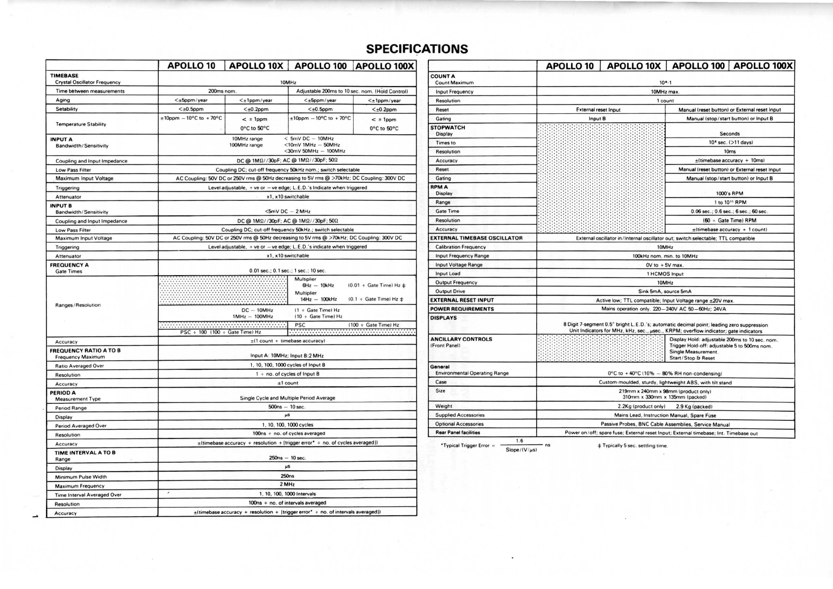
SPECIFICATION
INTRODUCTION
FUNCTIONAL DESCRIPTION
CIRCUIT DESCRIPTION
VOLTAGE CONVERSION
CALIBRATION
TROUBLE SHOOTING
AND
FAULT FINDING GUIDE
PARTS LIST
DIAGRAMS:
INDEX
MECHANICAL
ASSEMBLY
FUNCTIONAL BLOCK
DIAGRAM
COMPONENT
LAYOUT
MAIN PCB
COMPONENT
LAYOUT
PREAMP
PCB
COMPONENT
LAYOUT
FRONT PANEL
PCB
COMPONENT
LAYOUT
SUB BOARD
PCB
1
2
2
5
8
9
10
11
3
4
15
16
17
18
CIRCUIT
DIAGRAMS
1 POWER SUPPLY
19
©
1986
BLACK STAR
2 PRE-AMPLIFIER 20
3 FREQUENCY MULTIPLIER
21
PR
ES
CALER
4 INPUT SELECTOR 22
STOPWATCH
START/STOP
GATING
5 SLOPE CONTROLS 23
HOLD-OFF
SINGLE MEASURE PRIMING
TRIGGER L.E.D. CONTROL
RESET
DISPLAY HOLD
MAIN
COUNTER I.C.
6 SYSTEM CLOCK 24
RPM PRESCALER
7 FRONT PANEL SWITCH LOGIC 25
8 DISPLAY MULTIPLEXERS 26
RANDOM LOGIC
9 FRONT PANEL DISPLAYS 27
10
MISCELLANEOUS SWITCHING 28
TIMEBAS
E
Crystal Oscillator Frequency
Time
between
measurements
Aging
Setability
Temperature
Stability
INPUT
A
Bandwidth
/
Sensitivity
Coupling
and
Input
Impedance
Low
Pass Fitter
Maximum Input Voltage
Triggering
Attenuat
or
INP
UT
B
B
andwidth
/Sensitivity
Coupling and
Input
Impedance
Low
Pass Filter
Maximum
Input
Voltage
Triggering
Attenuator
F
REQU
EN
CY
A
Gate
Tim
es
Ranges/Resoluti
on
Accuracy
FREQU
ENCY
RA
T
IO
A TO B
Frequency
Maximum
Ratio Averaged Over
Resoluti
on
Ac
cu
ra
cy
PERIOD
A
Measurement Type
Per
io
d Range
Display
Period Averaged Over
Resol
uti
on
Ac
curacy
TIM
E
INTERVA
L A TO B
Range
Display
Minimum
Pulse Wi
dth
Maximum
Frequency
Time Interval Averaged Over
Resolution
Accuracy
SPECIFICATIONS
APOLLO 10 APOLLO
10X
APOLLO 100 APOLLO 100X
10MHz
200ms nom.
Adjustable
200ms to
10
sec.
nom
. (HOid
Contrell
<::t
5ppm
/year <::t
lppm
/
year
<::t
5Ppm
/
year
<:t
lppm
/year
<.0
.Sppm
<~
.2ppm
<.O
.Sppm
<:0
.2ppm
::t
10ppm -10°C
to
+ 70°C < z
lppm
::t
l()ppm -10°C to + 70°C <
::t
lppm
0°c
to
so
0c
0°c
to
so
0c
10MHz range <
SmV
DC -
10MHz
100MHz
range
<10mV 1MHz -00MHz
<
30mV
50MH
z - 100MHz
DC@
1
MU
//
30pF;
AC@
1M
{l
/ /30pF ;
SOU
Coupling DC; c
ut
-
off
frequency
S()kHz
nom
.;
switch
selectable
AC
Coupling
: 50V DC
or
250V
rm
s@
50Hz
decreasing
to
5V
rms@
>70kHz; DC
Coupling
: 300V DC
Level adjustable, + ve or
-ve
edge; L.E.D.·s Indicate
when
triggered
xl,
xl0
switchable
<SmV DC - 2 MHz
DC@
1M
{l
/ /30pF;
AC@
1MQ/ /30pF;
son
Coupling DC; c
ut
-
off
frequency
SOie.Hz
.; switch selectable
AC Coupling: 50V DC or 250V
rms@
50Hz decreasing to 5V
rms@
>70kHz; DC Coupling:
JOOV
DC
Level adjustable, +ve or -ve edge; L.E.D.'s indicate
when
triggered
xl
,
xl0
switchable
0.
01
sec.; 0.1sec .; 1sec. ;
10
sec.
·: ·::.·.·:::.·::.
·:::
·:
·::::
:::
:
Mult1pl1
er
6Hz - 10kHz
10
.
01
+ Gate Time)
Hz*
Mult
iplier
·::
14Hz -100kHz
10
.1 + Gate TimeI
Hz*
DC -10MHz (1 + Gate Time)
Hz
1MHz -100MHz I
10
+ Gate Time) Hz
..
...
..
.•:•:•
.
·.·.·
.
·.·.·.·.•.•:
·.
·
.·.
·
.·
.
·.·
.·
.·
.
·.·.·
.
-:·:·:
·:
·.
·.
I PSC (1()() +
Ga1e
Time) Hz
.... .
..
.
..
...
.
PSC +
100
1100
r Gate Time/
Hz
1
•·:·
·:
··
····
·
·············
·
··
·
·······
···
··::.·.·.
·..·.
·.·.·.·
.
·.·.·.·
.
·.·.·.·
.
·.·.·.
:t(1co
unl
+ timebase accuracy)
Input A: 10MHz; Input 8:2 MHz
1,
10
,
100,
1()))
cycles of Input B
1 +
no
.
of
cycles
of
Input
8
:tl
count
Single Cycle and Multiple Period Average
5(X)ns
- 10 sec.
-·
1,
10,
100,
1()))
cycles
100ns +
no
.
of
cycles averagect
:tltim
ebase accuracy + resolution + ltrigger error• +
no
.
of
cycles averagedI)
250ns -
10
sec.
-·
250ns
2 M
Hz
1, 10, 100, 1
()))
Intervals
lOOns
+
no
.
of
intervals averaged
:t(timebase accuracy + resolution + Itrigger
error•
+
no
.
of
intervals averagedII
APOLLO 10 I APOLLO 10X APOLLO 100 I APOLLO
100X
C
OUNT
A
Count
Maximum
Input Frequency
Resolution
Reset
Gating
S
TOPW
AT
CH
Display
Times
to
Resolution
Accuracy
Reset
Gating
RP
MA
Display
Range
Gate Time
Resolution
Accuracy
EXTE
RNAL
TI
ME
BASE OS
CILLA
TOR
Calibration Frequency
Input Frequen
cy
Range
Input Voltage Range
Input Load
Output
Frequency
Output
Drive
EXTE
RNAL
RESET
INPU
T
PO
W
ER
REQUIRE
MEN
TS
DI
SPLA
YS
ANCIL
LARY
C
ON
TROLS
(Front Panel)
Gene
ral
Environmental Operating Range
Case
Size
Weight
Supplied Accessories
Optional Accessories
Rear P
antH
facilities
1.6
•Typical Trigger Error = -
----
-ns
Slope/
(V
/
µsl
10•-1
10MHzmax
.
1
count
Fvternal reset Input Manual !reset
button)
or
External reset
Input
Input B Manual (stop/start
button
) or I
nput
B
. . . . . . . . ·. ·.
___
• Seconds
. , .
...
.;.::::
·:
::·:·... :.
..
:
._
____
_
,_o_•_••-~
-;.,,-1>_
~_,
_
da
_v_s_l
--------1
.·,·
•.
·..
t-
--
----
- -
---
-------1
:t(timebase accuracy + 10ms)
.........
..
..
. : : : . . . :
..
:-:
-
.·
.
Man
ual (reset
button)
or
External reset
Input
. : ·,· . .
,•
..·...
>------
-
----
---~--
Manual (stop/start
button)
or
I
nput
B
. .. . . .
.
,:,
.
:,
.
....
-:
-. . .:
.·
.
..
' , '
. : : . . . : : : : : . . . . . . .
~.
!:
~.
l()X)'s RPM
..
·,· . 1
to
10
11 RPM
..
·.• ·.·. .
...
.
..·
.•,•
.•,:-:-:: : :·: :
:-·
,•
0.06
se
c.; 0.6 sec.; 6 sec.;
6()
sec.
(60
+ Gate Time) RPM
..
:tltimebase accuracy + 1
count)
External oscillator in/Internal oscillator
out
;
swit
ch selectable;
TT
L compatible
10MHz
lOOkHz
nom
. min.
to
10MHz
0V
to
+ 5V max.
1HCMOS
Input
10MHz
Sink SmA, source SmA
Active
low
; TTL compatible; Input Voltage range
~V
max.
Mains operation only.
220
-240V AC
50-60Hz
; 24VA
8 Digit 7-segment
0.5'
' bright L.E.D.'s;
automati
c decimal
point
; leading zero suppression
Unit Indicators for MHz. kHz.
se
c ., µsec., KRPM;
overflow
indicator; gate i
ndi
cators
:: \ Display Hold: adjustable 200ms
to
10
sec.
nom
.
:!; :;; Trigger Hold-o
ff
: adjustable 5 to 500ms
nom
.
\
::>;:'.:'.
:;
:
~~:~~s~i=~r;::~t.
0°C
to
+ 40°C I
10
% - 80%
RH
non
-condensing)
Custom-moulded, sturdy,
lightweight
ABS
.
with
tilt stand
219mm x 240mm x 98mm (product only)
310mm x 330mm x 135mm (packed)
2.2Kg (produ
ct
only) 2.9 Kg (packed)
Mains Lead, Instruction Manual, Spare Fuse
Passive Probes. BNC Cable Assemblies, Service Manual
Power on/
off;
spare fuse; External reset Input; External timebase;
lnt
. Timebase
out
* Typi
ca
lly
5sec
. settling time.
INTRODUCTION
1.
HANDLING
While the APOLLO counter timers have been
designed
to
be
rugged, severe shocks can
be
des-
tructive and should
be
avoided. Do
not
expose
to
radiant heat, including direct sunlight
for
long
periods, or excessively high humidity. When ser-
vicing suitable precautions should
be
taken against
static discharge
as
the
unit
contains CMOS compo-
nents.
2.
TEST
EQUIPMENT
(a) Signal generators 2Hz
to
100MHz
with
cali-
brated output.
(bi
(cl
(d)
Frequency standard
with
an accuracy
of
0.05ppm or better.
Oscilloscope
with
100MHz bandwidth and
5mV
/div
sensitivity.
x10, 10M 01oscilloscope probe.
(el 3½ digit multimeter.
3.
DISMANTLING
(a) Remove TRIGGER LEVEL, HOLD and HOLD
FUNCTIONAL DESCRIPTION
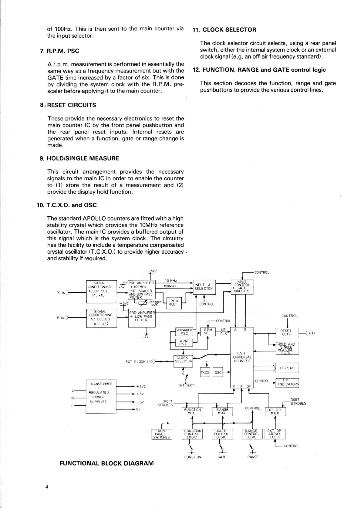
1.
INPUT
A
The signal at input A passes through the signal con-
ditioning circuit. This
is
the
x1
/x10 attenuator, A.C.
50
n and D.
C.
coupling circuits. The signal then
passes
to
the pre-amplifier where the signal
is
ampli-
fied, filtered by the
low
pass filter
if
required, and the
trigger level
is
adjusted.
The signal can then
follow
one
of
two
paths, (
1)
through a Schmitt trigger squaring circuit or
(2)
through an E.C.L. amplifier
to
provide a suitable
signal
for
the 100MHz pre-scaler.
The 10MHz
output
can
be
routed via the frequency
multiplier
to
achieve greater resolution when making
low
frequency measurements.
The three outputs from the input A amplifier are then
passed
to
the input A selector.
2.
INPUT
B
The signal at input B passes through identical signal
conditioning and pre-amplifier circuitry
as
input A,
with
the exception
of
the E.C.
L.
amplifier, 100MHz
pre-scaler and frequency multiplier circuits.
OFF
knobs by gently
but
firmly pulling
from
3.
INPUT
SELECTOR
shaft.
(b) Remove
tilt
stand by pushing firmly inwards on
one side.
(cl Unscrew the
four
recessed pozidrive screws set
into the feet on the underside
of
the case.
(di Gently separate the
two
case halves ensuring
the rear panel remains in the lower case half.
NOTE: If the counter only requires calibration no
further disassembly
is
necessary.
If
component
replacement
is
required then proceed
as
follows.
(e) Remove the four self-tapping screws securing
the main p.c.b.
to
the lower case half.
(f) Carefully
lift
the entire assembly including rear
panel from the lower case half.
(gl Desolder the GROUND connection between
the
front
and rear panels.
(h) Separate the rear panel from the main p.c.b. by
disconnecting PL401, PL100 and PL101.
(i) Separate the
front
panel assembly by pulling it
c.way
from
the main circuit board. Take care
not
to
bend the connector pins.
(j) The pre-amplifier p.c.b. can
now
be
removed
by gently pulling upwards. Take care
not
to
bend the connector pins.
(kl
Desolder the
two
B.N.C. connectors and the
GROUND connection from the rear
of
the
front
panel p.c.b.
(I) Remove the
front
panel
from
the
front
panel
p.c.b.
Disassembly
is
now
complete. Reassembly
is
the
reverse
of
disassembly.
2
This selects which signal
is
fed
to
the main counter
i.
e.
10MHz, 100MHz, frequency multiplier or stop-
watch pre-scaler output.
4.
INPUT
CONTROL CIRCUITS
This section contains the
start/stop
control logic, the
hold
off
monostable, single measure priming circuit,
slope selection and input A gating circuit.
5.
MAIN
COUNTER INTEGRATED CIRCUIT
This
is
a fully integrated Universal counter and
display driver. It contains all the circuitry necessary
to
function
as
afrequency counter, a period counter,
a unit counter, a frequency ratio counter and a time
interval counter.
The
FUNCTION,
RANGE,
CONTROL
and
EXTERNAL DECIMAL POINT inputs are time multi-
plexed
to
select the desired input function. This is
done by connecting the appropriate digit strobe
to
the control inputs
F,
Rand
DP
. The control
of
these
inputs
is
done by the FUNCTION, RANGE and
EXTERNAL
DP
multiplexers, which are in turn con-
trolled by the various CONTROL LOGIC circuits and
front
panel switches.
6.
STOPWATCH PSC
In
order
to
provide the counter
with
a stopwatch
function the counter
is
set
to
the count mode. The
internal 10MHz reference oscillator
is
divided
down
by the stopwatch pre-scaler
to
produce a frequency

ov
z
~
0
er
Q)
GREEN /YELLOW
WHITE
I
WHIT
MECHANICAL ASSEMBLY
LJ
LJ
SK12O3 SK12O2
MAIN
P.
C. B.
I
PRE -AMP PRESCALER
ANO FREQUENCY
MULTIPLIER
P.C
.B.
C4O2
G)
TC.XO
.
ADJUST
LJ'
PL12O1la)
PL12O1lb)
al
u
a.:
...J
UJ
z
rt
I-
z
0
er
u.
R1269
.L
of
100Hz. This
is
then sent
to
the main counter via
the
input
selector.
7. R.P.M. PSC
A r.
p.m.
measurement
is
performed in essentially the
same
way
as
a frequency measurement
but
with
the
GATE time increased by a
factor
of
six. This
is
done
by dividing the system clock
with
the R.P.M. pre-
scaler before applying
it
to
the main counter.
8.
;RESET
CIRCUITS
These provide the necessary electronics
to
reset the
main counter
IC
by the
front
panel pushbutton and
the rear panel reset inputs. Internal resets are
generated when a
function
, gate or range change
is
made.
9.
1HOLD/SINGLE
MEASURE
This circuit arrangement provides the necessary
signals
to
the main
IC
in order
to
enable the counter
to
(
1)
store the result
of
a measurement and
(2)
provide the display hold
funct
ion.
10. T.C.X.O. and OSC
The standard APOLLO counters are fitted
with
a high
stability crystal
which
provides
the
10MHz reference
oscillator. The main
IC
provides a buffered
output
of
this signal
which
is
the system clock. The circuitry
has the facility
to
include a temperature compensated
crystal oscillator (T.C.X.O.)
to
provide higher accuracy .
and stability
if
required.
SIGNAL
CO
NDITIONING
'
t{,
IN
------1
AC.DC,
50.fl
x1
, x10
+5V2
11. CLOCK SELECTOR
The clock selector circuit selects, using a rear panel
switch, either the internal system clock or an external
clock signal
(e
.g.
an
off-airfrequency standard).
12.
FUNCTION,
RANGE and GATE control logic
This section decodes the
function,
range and gate
pushbuttons
to
provide the various control lines.
INPUT
CO
NTROL
+ GATE
CIRCUITS
CO
NTR
OL
SIGNAL
,8, IN
-----<
CONDITIONING
AC
oc,
son
X1. X 10
PR
E- AMPLIFIER
f--------+-----'
4
TRANSFCJR,,1ER
+
REGULATED
N POWER
SUPPLIES
E
+
LO
W
PASS
F
IL
TER
- 5V
EXT
CLOC
K
1/0
......,
..........
_
+5V2
+sv
-s
v
ov
DIGI T
STROBES
F
RON
T
PA
NE
L
SWITC
HE
S
FUNCTIONAL
BLOCK
DIAGRAM
FUNCT
IO
N GATE
A B
L.S.
l.
UNIVERSAL
CO
UNTER
RANGE
CO
NTR
OL
DISP
LAY
DIGIT
STROBES
CONTROL
EX
T
CIRCUIT DESCRIPTION
The following description applies
to
the APOLLO
100
counter timer. Certain sections
are
not applicable
to
the
APOLLO
10.
Refer
to
circuit diagrams for the differ-
ences. NOTE control signals marked with
a'
*' are active
low
e.g. (*
FREQ)
.
1.
POWERSUPPLY(CCT. DIAG.1)
Three separate voltages
are
generat
ed
by the power
supply circuit. These voltages
are
provided by mono-
lithic integrated circuit regulators IC100,
101,
102
and
their associated components. The +5V2, and the
-
5V
supplies
are
used by the pre-amplifier, pre-
scaler and frequency multiplier circuits. The +5V2
supply
is
adjusted by RV100
to
5.2V ±0.05V so that
the
ECL
circuits operate at their optimum voltage.
The +
5V
supply
is
used by the main logic circuits.
Test points TP100,
TP101
, TP102 and TP103
are
pro-
vided for convenient monitoring
of
the power
supplies. All three voltage supplies have built in short
circuit protection. The mains transformer T100 pro-
vides the necessary voltage conversion and isolation
of
the mains supply voltage. Transformer taps are
provided
to
enable conversion
to
110/120V
operation.
Fuse
F100
provides protection against
fault currents. SW100
is
the instrument ON/OFF
switch arid
is
mounted on the rear panel.
2.
PRE-AMPLIFIERS (CCT. DIAG.
2)
S1200 selects the input coupling mode AC,
50
n,
DC
or LPF.
With
the switch in the
50
n position
C1201
and
R1200
terminate the input
with
nominally
50
n,
(the input
is
DC
coupled in this position).
With
DC
selected the input signal
is
directly coupled
to
the
pre-amplifier.
R1201
sets the input impedance
to
1
Mn.
With
S1201
in
the x10 position the input signal
passes through the x10 attenuator,
R1202
and
R1203
perform the voltage division and C1202 and
C1203
provide frequency compensation.
The pre-amplifier
is
protected from excessive input
voltage by
R1204
,
R1239
,
C1204
, D1200, and D1201.
The input coupling components are situated on the
front
panel sub-board, which
is
mounted between
the
front
panel and the
front
panel p.c.b.
01200, 01201 and 01202 form a high input impe-
dance, wide bandwidth voltage follower. The high
input impedance
is
necessary
to
avoid loading the
input coupling and attenuator circuits.
The next stage
of
the pre-amplifier consists
of
two
differential amplifiers 01208, 01209 and 01206,
01207. Amplifier 01206, 01207
is
operative when the
LPF
(low pass filter)
is
selected. Amplifier 01208,
01209
is
operative when AC,
500
or
DC
is
selected.
Normally 01205
is
biased on so that the current
source 01203
is
connected
to
the emitters
of
01208,
01209, so that this amplifier
is
operative. Alterna-
tively
if
the
LPF
is
selected 01204
is
biased on and
01205
is
biased
off
so that the current source
is
con-
nected
to
the emitters
of
01206 and 01207. This
amplifier
is
then operative and the inputsignal passes
through the
low
pass network
R1213
and
C1205
before amplification. The filter components values
are
calculated
to
give a cut
of
frequency
of
nominally
50kHz.
The variable resistor
R1218
is
the front panel
TRIGGER
LEVEL
control and sets the working point
of
the differential amplifiers. Resistor
R1219
is
adjusted during calibration
to
take account
of
com-
ponent tolerances. The emitter follower 01210
applies the working point voltage
to
the
base
of
01206, 01207, 01208, 01209. Diodes D1204 and
D1205
provide temperature compensation
for
the
trigger level control.
The antiphase outputs from the differential amplifier
provide the input
to
IC1200(b). IC1200(b) forms the
main gain stage
of
the pre-amplifier, this
IC
is
an
ECI
differential line driver biased
to
operate
in
the linear
mode
to
provide higher gain. The output from
IC1200(b) feeds
two
circuits
(1)
a Schmitt trigger
ECL
to
TTL converter, 01211, 01212 and 01213. 01213
is
a high speed switcliing transistor
to
ensure the
fastest possible
rise
time. Overall feedback around
this amplifier
is
provided by
R1229
.
(2)
IC1200(c)
buffers the output
of
IC1200(b)
to
provide asignal for
the 100MHz pre-scaler
(see
CCT. DIAG. 3).
3.
FREQUENCY MULTIPLIER
AND
PRE-SCALER
CIRCUITS (CCT. DIAG.
3)
IC1105
is
a +
10
or +
11
pre-scaler.
D1103
pulls pins 2
and 3 high
to
set the pre-scaler
to
the
+-10
mode.
The 10MHz
output
from the pre-scaler
is
inverted by
the Schmitt trigger IC1106(b) and sent
to
the input
selector
(see
CCT. DIAG. 4).
Channel A output from 01213
(see
CCT. DIAG.
3)
is
inverted by IC1106(f) and sent
to
the input selector.
The channel B signal from the pre-amplifier
is
passed
through IC1106(a,c) and sent
to
the Gating and Input
B circuits
(see
CCT. DIAGS.
4and
5).
IC1101
performs level shifting for the input signals
to
the frequency multiplier circuit. This
is
necessary
as
the frequency multiplier circuit operates from dual
supplies. The frequency multiplier function
is
per-
formed by IC1102, IC1103, IC1104 and associated
components, which form a frequency multiplying
PHASE LOCKED LOOP. IC1102
is
a phase locked
loop integrated circuit, containing
two
phase com-
parators, a voltage controlled oscillator (VCO) and a
source follower. IC1103
is
a
two
stage counter which
divides the VCO output by either
10
or
100
and sends
the signal
to
the phase comparator input pin
3.
The
two
multiplier ranges
are
selected by the control lines
(* 100kHz) and (* 10kHz). When the 10kHz range
is
selected the gate IC1104(a)
is
enabled and the divide
by
100
output
of
IC1103
is
sent
to
the phase com-
parator input of IC1102
to
provide a multiplication
factor
of
100.
When the 100kHz range
is
selected the
gate IC1104(b)
is
enabled and the divide by
10
output
from IC1103
is
sent
to
phase comparator input of
IC1102
to
provide amultiplication factor of
10.
The phase comparator
output
(PC
OUT)
is
smoothed
by the filtering components
R1107, R1108,
R1116
,
C1102
and
C1103
to
provide the control voltage for
5
the voltage controlled oscillator (VCO IN). NOTE
C1102, C1103 and R1116 are only in circuit when the
10kHz range is selected, these components are
required
to
reduce the
amount
of
ripple on the VCO
control voltage when making low frequency measure-
ments
to
ensure a stable display.
The (FM 1NH) signal
(see
also CCT. DIAG.
8)
is
used
as
the enable
for
the multiplier function. When either
the 10kHz or 100kHz range
is
selected
the(*
FM INH)
signal goes high and turns
off
TR1101 causing the
voltage at pin 5
of
IC1102
to
go
low
and enable the
frequency multiplier. TR1102 ensures
that
the filter
capacitors C1102 and C1103 are fully discharged and
that
the VCO
is
operating
at
its lowest frequency
when the multiplierfunction
is
selected.
4.
INPUT
SELECTOR (CCT. DIAG.
4)
The INPUT SELECTOR selects
which
of
the input
signals, 10MHz, 100MHz, FM
or
STOPWATCH
is
sent
to
the main counter
for
measurement. IC304
is
a
1
of
8 data selector, the three control signals A,
B,
C
determine
which
of
the inputs are transmitted to the
output
(A IN).
The table below shows
how
the various functions are
selected.
C
H
L
L
L
B
H
H
L
H
A
H
L
H
H
w
07
02
01
03
FUNCTION
100MHz
10MHz
FM (multiplier)
STOPWATCH
5.
STOPWATCH
PSC (CCT. DIAG.
4)
IC307, IC308 and IC309
form
the stopwatch pre-
scaler circuit. The purpose
of
this circuit
is
to
provide
an accurate 100Hz signal
from
the 10MHz system
clock (SYS CLK)
that
can then be counted by the
main counter
IC
. IC307, IC308 and IC309
are
dual + 2
and + 5 counters. IC307 and IC308 are arranged
to
each divide
100
and IC309
to
divide by
10
to
give a
total division by 100,000.
The counters are provided
with
a clear signal, which
is
derived
from
the (RESET) line. The (CLEAR) signal
ensures
that
counting always begins on the same
signal edge so
that
counting errors are avoided.
6.
START/STOP and
GATING
(CCT. DIAG.
4)
The
START
/STOP
button
controls the stopwatch
and
count
functions. The start/stop circuit generates
two
signals when the start/stop
button
is
pressed,
(
1)
the Q
output
of
IC306 (pin
5)
and
(2)
the (START)
signal
from
IC708d. IC305 and IC306 give a toggle
action
to
the start/stop
button
(S1007). When the
(START) signal
is
high and
(*STOPW
+ COUNT)
is
low
then (GATE)
is
low,
which opens the input A
gate and allows counting or timing
to
begin (see Fig.
5)
. IC306
is
provided
with
a (RESET) signal
to
close
the input A gate and reset the
count
or stopwatch
when a reset occurs. The (START) signal
is
also used
to
prime the counter when using the single measure
facility.
6
7. SLOPE CONTROLS and HOLD-OFF (CCT. DIAG.
5)
The input signals (AIN) and (BIN) pass through the
exclusive
OR
gates IC200. Switches ATRIG and
BTRIG, the SLOPE controls, invert the signals
to
set
the trigger edge
to
+
VE
or -
VE
slope. When the
control signal (GATE)
is
low
IC202b passes the signal
through
to
be measured
by
the main counter IC.
signal through
to
be measured by the main counter
IC.
When making time interval measurements
it
is
some-
times necessary
to
delay the triggering
of
input B to
avoid triggering problems. This trigger hold
off
facility
is
accomplished by IC201, IC209 and their
associated components.
IC201
is
a precision CMOS
timer configured
as
a monostable. The monostable
period
is
set by the
front
panel hold
off
control
RV1001
and C200. The timing range
of
the hold
off
control
is
from nominally 5ms
to
500ms. The mono-
stable
is
triggered on by the negative going edge
of
the (AIN) signal via
C213
.
8.
SINGLE MEASURE
PRIMING
(CCT. DIAG.
5)
Before making a single time interval measurement
the main counter IC205 must
be
"primed".
This
is
done by generating a negative signal edge at AIN
(pin
40)
followed by a negative signal edge
at
BIN
(pin 2). The priming signals are generated by the shift
register IC203. The (START) signal
is
clocked
through the shift register by the system clock and
outputs are taken
from
pins 3 and
11
to
provide the
priming signals. The (SINGLE CYCLE) signal clears
the shift register prior
to
priming.
9.
TRIGGER LED CONTROL(CCT. DIAG.
5)
The
front
panel trigger level LED's are driven by
signals derived from the signal inputs;
to
the main
counter IC205. The B signal
is
first inverted by
IC204b and then sent
to
the display p.c.b. The gate
arrangement IC208, 204 selects the (10M INP) signal
when the frequency multiplier function
is
active, this
ensures
that
the input A trigger
LED
flashes
at
the
same rate
as
the signal being measured and
not
at
the multiplied rate
of
the frequency multiplier output.
10. RESET (CCT. DIAG.
5)
The RESET circuitry enables the user
to
set the
display
to
zero and prepare the counter
for
the next
measurement.
Two
user resets are provided, (
1)
the
front
panel pushbutton and,
(2)
the rear panel input
sockets. The
front
panel reset
is
performed by
S1003.
When
this button
is
pressed, pin
19
of
IC205
is
pulled
low
, this resets the main counter. Note the
reset signal is also sent
to
other parts
of
the counter
circuit
to
perform various necessary resets.
When
the rear panel reset input
is
pulled
low
TR206
is
turned
off
allowing TR205
to
turn on
which
pulls
the reset line
low
to
perform a reset. When the reset
signal is removed TR206
is
turned on via
R207
and
R213
which
allows the reset line
to
return high.
Protection up
to
± 20V
is
provided by D201,
D203
an
D204,
with
the input current limited by R207.
An
internal reset
is
generated by the
front
panel
switch logic, this resets the counter whenever a
range
of
function change
is
made.
11.
DISPLAY HOLD (CCT. DIAG.
5)
The display hold "freezes" the last measurement
made on the display.
Two
separate functions are
available (
1)
a variable display hold and
(2)
an
indefi-
nite display hold. The variable hold
is
performed by
the monostable IC201.
After
the main
IC
has per-
formed and displayed the result
of
a measurement,
the STORE
output
of
IC205 goes
low
and triggers the
mon,ostable. The Q
output
of
IC201
passes via the
NOR
gate IC206 and sets the following
RS
latch
IC206(a,b)
output
high, this causes IC205
to
"freeze"
the display.
At
the end
of
the monostable timing
period the
RS
latch is reset and the counter makes
the next measurement. RV1000 and C206 adjust the
HOLD time between nominaly200ms and
10s.
When the
front
panel HOLD button
is
pressed the
RS
latch
output
is
set high and thedisplay
is
held indefi-
nitely. When the single measure
button
is
depressed
the monostable
output
sets the
RS
output
high and
causes IC205
to
"freeze"
the display until the counter
is
reset.
12.
MAIN
COUNTER IC (CCT. DIAG.
5)
IC205
is
a fully integrated universal counter and dis-
play driver. It contains all the circuitry necessary
to
function
as
a frequency counter, a
unit
counter, a
frequency ratio counter and a time interval counter.
The FUNCTION, RANGE, CONTROL and EXTER-
NAL
DECIMAL POINT inputs are time multiplexed
to
select the desired input function. This
is
done by
connecting the appropriate digit strobe (01
to
D8)
to
the control inputs. The control
of
these inputs
is
achieved by the function, range and external decimal
point multiplexers
(see
CCT. DIAG. 8), which are in
turn controlled by the various control and logic cir-
cuitryand
front
panel switches.
A display test facility
is
provided, which
is
activated
by connecting together pins 1 and 2
of
PL202. PL202
is
situated on the main p.c.b. The display test illumi-
nates all the display segments and all decimal points
except decimal point8.
13.
FRONT PANEL
SWITCH
LOGIC ,(CCT. DIAG.
7)
Resistors
R701
to
R703
and capacitors
C701
to
703
in
conjunction
with
IC708(a,b,c) ensure that the set up
times
of
the following
J-K
flip flops are met.
IC701
and IC702
are
clocked by the (SLO CLK) and produce
a single pulse
of
1ms duration each time FUNCTION,
FREQ
or GATE buttons are pressed. Diodes D701,
D702, D703 and TR700 form a three input
NOR
gate
which generates a reset whenever the FUNCTION,
RANGE or GATE
button
is
pressed. The next stage
of
the circuit
is
the Programmable Array Logic (PAL).
IC703. This
IC
is
a fusible link
AND
-
OR
gate array,
and
is
used
to
perform the complex logic functions
necessary
to
decode the FUNCTION, RANGE and
GATE switches. The advantage
of
using this device
is
that it replaces many discreet IC's and therefore
allows a more compact design.
The function
of
IC703 can
be
divided into three
sections (
1)
the FUNCTION logic,
(2)
the RANGE
logic and
(3)
the GATE logic.
The FUNCTION outputs 014, 013,
012
of
IC703
is
a
3 bit binary code which increments by one each time
the FUNCTION button
is
pressed. IC704
is
a 3
to
8
line decoder which decodes the PAL outputs
to
provide the seven function control lines: (*FREQ),
(*RATIO), (*TIME INT), (*COUNT), (*RPM),
(*STOPWATCH) and (*PERIOD).
The RANGE outputs 019, 018,
017
are
decoded by
IC705
to
give the five frequency range control lines:
(*10M), (*100M), (*10kHz), (PSC) and (*100kHz).
The GATE outputs
015
and
016
are decoded by
IC706
to
provide the four GATE control lines:
(*1SEC), (*10SEC), (*100ms) and (*10ms).
Note that when either the stopwatch or count func-
tions are selected the control lines from IC706 are
inhibited by the (*STOPW+COUNT) control line.
The PAL has its
own
"power
up reset" circuit
R705,
C700
and D700. This ensures that when the counter
is
first switched on the RANGE
is
set
to
10MHz, the
GATE
is
set
to
1sec and the FUNCTION set
to
FRE-
QUENCY.
IC707 provides the correct decimal point positioning
for
all possible combinations
of
selected function
range and gate time. IC707
is
a fusible link ROM
(read only memory)
with
its address lines connected
to
the PAL outputs. The ROM data lines are the deci-
mal point control signals (DPC), (DPD), (DPC).
14.
RANDOM
LOGIC and DISPLAY MULTIPLEXERS
(CCT. DIAG.
8)
The random logic circuitry generates various control
signals from the 1
of
8 decoders IC704, IC705, IC706.
One example
is
the (*FM INH) signal which
is
used
to
enable the frequency multiplier circuit when either
the 10kHz or 100kHz frequency range
is
selected.
As described in section
12
the FUNCTION and
RANGE selection
is
accomplished by connecting the
appropriate digit drive
to
the control inputs
of
the
main counter IC. IC804 and IC805 perform this
function.
IC804 and IC805 are 8 channel analog multiplexers
which form digitally controlled single pole 8-way
switches which are controlled by the switch function
logic control signals.
See
over
for
table showing the functions selected by
each digit
for
the control input.
7

FUNCTION
Frequency
Period
Function Frequency Ratio
Pin
4 Time Interval
Unit Counter
Oscillator Frequency
0.01
Sec/ 1 Cycle
Range Input
0.1
Sec/10 Cycles
Pin
21
1 Sec/
100
Cycles
10
Sec/1k Cycles
Pin
31
Enable External Range
Input
Display
Off
Display Test
Control Input 1MHz Select
Pin 1 External Oscillator
Enable
External Decimal Point
Enable
DIGIT
D1
D8
D2
D5
D4
D3
D1
D2
D3
D4
D5
D4
and
Hold
D8
D2
D1
D3
External Decimal point output
is
for same digit
Decimal Point that
is
connected
to
this input
Input, Pin
20
15.
SYSTEM CLOCK and R.P.M. PRE-SCALER
(CCT. DIAG.
6)
In the standard model the 10MHz system clock
is
provided by the crystal oscillator circuit XTAL
400,
C400,
C401,
C402
and
R407.
Frequency adjustment
is
provided by trimmer capacitor
C401.
The clock signal
for
IC205
is
not provided directly by
the on chip oscillator but
via
the EXT
OSC
IN, this
allows for the provision
of
a T.C.X.
O.
(Temperature
Compensated Crystal Oscillator) or an externally con-
nected oscillator via the rear panel B.N.C. connector.
The gate arrangement
IC401
(a,b,
c)
selects either the
BUFF OSC OUT signal via IC401(d)
OR
the externally
applied oscillator signal EXT
OSC
IN. The output
from pin 6 of
IC401
is
pre-scaled by the divide by six
counter IC402
to
give a frequency
of
1.6667MHz
necessary for the
RPM
function. IC403 selects either
the 10MHz signal from pin 6
of
IC401
or the pre-
scaled output
of
IC402 which provides the clock
inputfor IC205.
The 10MHz
output
from
IC401
pin 3
is
buffered by
IC400 which then drives the switching transistor
TR401. The 4 gates
in
IC400 are connected
in
parallel
to
ensure that there
is
adequate drive for
TR401
. To
set the rear panel B.N.C. socket
to
an
output the rear
panel INT/EXT switch
is
set
to
the INT position, this
turns on the current mirror formed by TR402 and
TR400 which provides collector current for TR401.
To set the B.N.
C.
socket
to
an
input the switch
is
set
to
the
EXT
position, this turns
off
TR401
by pulling
the collector
of
TR402 high
via
R403
and
R410.
Gate
IC401
(a)
is
closed and Gate
IC401
(c)
is
opened allow-
ing
an
externally applied signal
to
be routed
to
the
main counter
IC
.
8
MIP output; this
output
from the main counter IC205
is
used to drive the front panel GATE
LED
and indi-
cates that a measurement
is
in
progress.
When using the STOPWATCH or COUNT mode or
if
the input signal
is
gated by input B then the (GATE)
signal controls the GATE
LED
which then illuminates
when counting or timing
is
in
progress. IC207(b,c)
and associated components form a pulse stretching
circuit that ensures that the GATE
LED
is
visible even
when the measurement cycle
is
short.
16
. FRONT PANEL DISPLAY SECTION (CCT. DIAG.
9)
IC's
600
,
601,
602
and
603
provide buffering
for
the
various control signals
to
drive the front panel LED's.
TR600 and
TR601
drive the overflow
LED.
17.
CONVERTING FROM 220/240V
to
110/120V
OPERATION
IMPORTANT -Disconnect Mains
Lead
Referring
to
DISMANTLING Section
3,
page
2,
disas-
semble up
to
Section 3(d).
Referring
to
MECHANICAL ASSEMBLY DIAGRAM,
page
3:
1.
On
transformer primary terminals, remove 0V
to
120V
link.
2.
Using 16/0.1 insulated wire, connect the
two
0V
terminals together, and connect the
two
120V
terminals together.
3.
Replace 250mA anti-surge fuse with 315mA
anti-surge fuse (and replace spare).
4.
Fit label
to
back panel indicating voltage and
fuse type.
CALIBRATION
1.
In order
to
calibrate the APOLLO series
of
counter
timers
it
is
first necessary
to
dismantle the
case
(see
Introduction p. 2).
2.
POWER SUPPLY
The first step in calibrating the instrument
is
to
ensure
that
the + 5V2 supply
is
set
to
within its
design limits
of
±0.05V.
If adjustment
is
required,
use a digital voltmeter and adjust RV100 until the
supply
is
within the required limits.
3.
TRIGGER LEVEL calibration (see diagram p.
3)
(a)
Centre both TRIGGER LEVEL controls
as
accurately
as
possible.
(b) Set both ATTENUATION switches
to
x1
.
(c) Set both COUPLING switches
to
A.C.
(d) Carefully adjust
R1219
until both input A trigger
LED's are illuminated.
(e) Carefully adjust
R1269
until both input B trigger
level LED's are illuminated.
4.
CRYSTAL CLOCK calibration (standard model)
Calibration
of
the crystal oscillator becomes
necessary
is
crystal
drift
exceeds requirements.
(a) Switch on the instrument and allow at least a
30
minute warm
up
period before proceeding.
(b) Set INPUT A COUPLING
to
AC.
(c) Set INPUT A ATTENUATION
to
x1.
(cl Set FUNCTION
to
FREQ.
(e)
Set GATE time
to
1s.
If) Set RANGE
to
10MHz.
(g) Connect a frequency standard
of
known
accuracy (0.1ppm or better)
to
INPUT A.
Typically a 10MHz off-air standard would
be
used.
(hi
Adjust TRIGGER LEVEL control until a stable
reading
is
displayed.
(i) Adjust
C401
for
a reading
of
10,000000 ± 5
digits.
5.
T.C.X.O. calibration
(a) Proceed
as
section 3 steps
(a)
to
(f).
(b) Connect a frequency standard
of
known
accuracy (0.05ppm or better)
to
INPUT A.
Typically a 10MHz off-air standard would
be
used.
(cl Adjust a TRIGGER LEVEL control until a stable
reading
is
displayed.
(d) Adjust T.X.C.O.
for
a reading
of
10.000000 ± 2
digits.
9
TROUBLE SHOOTING
AND
FAULT
FINDING
GENERAL
Check all control settings before assuming the instru-
ment
is
fa:..ilty. In particular the position
of
the
SINGLE MEASURE, HOLD, HOLD OFF, LPF, TRIG-
GER
LEVEL, and rear panel INT OUT
/EXT
IN
con-
trols.
Check
that
the correct fuse
is
fitted: 20mm 250mA
anti-surge. NO OTHER TYPE SHOULD
BE
USED.
When
replacing components always use a part
of
the
specified type and tolerance. This
is
not
just a matter
of
accuracy,
but
often a specified component will
have improved stability and thermal performance
compared
to
superficially similar items.
It
is
particu-
larly important
that
transistors are replaced
with
the
specified item otherwise performance may be
degraded.
It
is
always advisable
to
re-calibrate the instrument
after servicing
to
ensure
that
the performance
is
within
specification.
POWER SUPPLIES
A faulty
power
supply can cause a variety
of
faults.
Use test points TP100,
TP101
and TP102
to
check
the supply voltages.
It
is
particularly important
that
the 5V2 supply
is
set
to
5V ±0.05V.
PRE-AMPLIFIERS
The pre-amplifiers
do
not
normally cause problems.
If
however any components associated
with
the dif-
ferential amplifiers are changed then re-calibration
of
the trigger level controls
is
essential.
OSCILLATOR
If
the crystal oscillator fails this
is
immediately
apparent
as
only one digit lights up
with
very high
intensity. The oscillator should be monitored
with
an
oscilloscope at pin
38
of
the main counter IC205.
If
no 10MHz signal
is
present then suspect the crystal
XTAL400,
(orT.C.X.O.
if
fitted).
DISPLAY
The display digit strobes are used
for
control
of
the
counter's functions and leakage between the very
fine tracks can cause a variety
of
function
and display
problems, including
"ghosting
of
display segments".
EXTERNALREFOSCINPUT
This
input
is
TTL
compatible, ensure
that
signal
source used has a compatible
output
level. Check
that
frequency
of
reference signal
is
within
the range
100kHz
to
10MHz. The calibration frequency
is
10MHz, if other frequences
are
used then the measure-
ment cycle time will increase accordingly and the dis-
play multiplexing rate will decrease.
10
SWITCH CONTROL LOGIC
A lack
of
response
to
the function, range and gate
switches
is
indicative
of
a fault in the switch control
logic, this
is
most commonly caused by IC703 (PAL),
or a failure
of
the (SLO CLK) signal. Check
that
the
'Q'
outputs
of
IC703 respond
to
the function, range
and gate switches and
for
the presence
of
the clock
signal
at
pin 1
of
IC703.
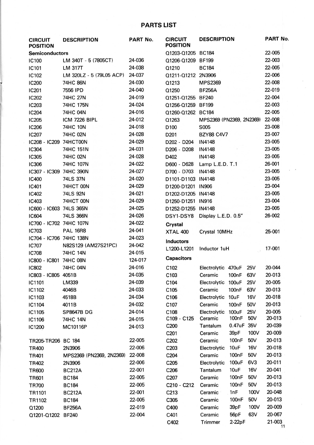
PARTS LIST
CIRCUIT DESCRIPTION PART No. CIRCUIT DESCRIPTION PART No.
POSITION POSITION
Semiconductors 01203-01205 BC184 22-005
IC100
LM
340T - 5 (7805CT) 24-036 01206-01209 BF199 22-003
IC101
LM
317T 24-038 01210 BC184 22-005
IC102
LM
320LZ - 5 (79L05 ACP) 24-037 01211-01212 2N3906 22-006
y IC200 74HC 86N 24-030 01213 MPS2369 22-008
IC201
7556 IPD 24-040 01250 BF256A 22-019
IC202 74HC 27N 24-019 01251-01255 BF240 22-004
IC203 74HC 175N 24-024 01256-01259 BF199 22-003
IC204 74HC 04N 24-016 01260-01262 BC184 22-005
IC205 ICM 7226 BIPL 24-012 01263 MPS2369 (PN2369, 2N2369) 22-008
IC206 74HC 10N 24-018 D100 S005 23-008
IC207 74HC 02N 24-028
D201
BZY88 C4V7 23-007
IC208 -IC209
74HCTOON
24-029 D202 -D204 IN4148 23-005
IC304 74HC 151N 24-031 D206 -D208 IN4148 23-005
IC305 74HC 02N 24-028 D402 IN4148 23-005
IC306 74HC 107N 24-022 D600 -D628 Lamp L.E.D. T.1 26-001
IC307 -IC309 74HC 390N 24-027 D700 -D703 IN4148 23-005
IC400 74LS 37N 24-020 D1101-D1103 IN4148 23-005
IC401 74HCT
OON
24-029 D1200-D1201 IN906 23-004
IC402 74LS 92N 24-021 D1202-D1205 IN4148 23-005
IC403 74HCT
OON
24-029 D1250-D1251 IN916 23-004
IC600 -IC603 74LS 365N 24-025 D1252-D1255 IN4148 23-005
IC604 74LS 366N 24-026
DSY1-DSY8
Display L.E.D.
0.5"
26-002
IC700 -IC702 74HC 107N 24-022 Crystal
IC703
PAL
16R8 24-041
XTAL
400 Crystal 10MHz 25-001
IC704 -IC706 74HC 138N 24-023 Inductors
IC707 N82S129 (AM27S21PC) 24-042 L1200-L1201
Inductor
1uH 17-001
IC708 74HC 14N 24-015
ICBOO
-IC801 74HC 08N 124-017 Capacitors
IC802 74HC 04N 24-016 C102 Electrolytic 470uF 25V 20-044
IC803 -IC805
4051
B 24-035 C103 Ceramic 100nF 63V 20-013
IC1101 LM339 24-039 C104 Electrolytic 100uF 25V 20-005
IC1102 4046B 24-033 C105 Ceramic 100nF 63V 20-013
IC1103 4518B 24-034 C106 Electrolytic 10uF 16V 20-018
IC1104 4011B 24-032 C107 Ceramic 100nF 50V 20-013
IC1105 SP8647B DG 24-014 C108 Electrolytic 100uF 25V 20-005
IC1106 74HC 14N 24-015 C109 -C125 Ceramic 100nF 50V 20-013
IC1200 MC10116P 24-013 C200 Tantalum 0.47uF 35V 20-039
C201
Ceramic 39pF 100V 20-009
TR205-TR206 BC 184 22-005 C202 Ceramic 100nF 50V 20-013
TR400 2N3906 22-006 C203 Electrolytic 10uF 16V 20-018
TR401 MPS2369 (PN2369, 2N2369) 22-008 C204 Ceramic 100nF 50V 20-013
TR402 2N3906 22-006 C205 Electrolytic 100uF 6V3
20-011
TR600 BC212A 22-001 C206 Tantalum 10uF 16V 20-041
TR601 BC184 22-005 C207 Ceramic 100nF 50V 20-013
TR700 BC184 22-005 C210 -C212 Ceramic 100nF 50V 20-013
TR1101 BC212A 22-001 C213 Ceramic 1nF 100V 20-048
TR1102 BC184 22-005 C305 Ceramic 100nF 50V 20-013
01200
BF256A 22-019 C400 Ceramic 39pF 100V 20-009
01201-01202
BF240 22-004
C401
Ceramic 56pF 63V 20-067
C402
Trimmer
2-22pF 21-003
11
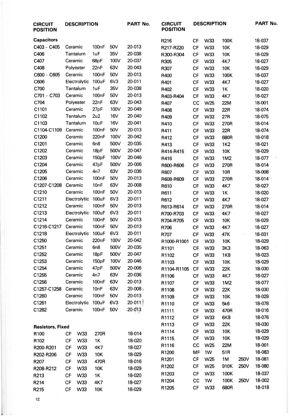
CIRCUIT DESCRIPTION PART No. CIRCUIT DESCRIPTION PART No.
POSITION POSITION
Capacitors R216
CF
W33
100K 18-037
C403 -C405 Ceramic 100nF 50V 20-013 R217-R220 CF
W33
10K 18-029
C406
Tantalum
1uF 35V 20-038 R300-R304 CF
W33
10K 18-029
C407 Ceramic 68pF 100V 20-037 R305
CF
W33
4K7 18-027
C408 Polyester 22nF 63V 20-043 R307 CF
W33
10K 18-029
C600 -C605 Ceramic 100nF 50V 20-013 R400 CF
W33
100K
18
-037
C606 Electrolytic 100uF 6V3 20-011
R401
CF
W33
4K7 18-027
C700
Tantalum
1uF 35V 20-038 R402 CF
W33
1K 18-020
C701
-C703 Ceramic 100nF 50V 20-013 R403-R404
CF
W33
4K7 18-027
C704 Polyester 22nF 63V 20-043 R407 cc
W25
22M 18-001
C1101 Ceramic 27pF 100V 20-049 R408 CF
W33
22R 18-074
C1102
Tantalum
2u2 16V 20-040 R409
CF
W33
27R 18-075
C1103
Tantalum
10uF 16V 20-041 R410
CF
W33
270R 18-014
C1104-C1109 Ceramic 100nF 50V 20-013
R411
CF
W33
22R 18-074
C1200 Ceramic 220nF 100V 20-042 R412 CF
W33
680R 18-018
C1201 Ceramic 6n8 500V 20-035 R413
CF
W33
1K2 18-021
C1202 Ceramic 18pF 500V 20-047 R414-R415
CF
W33
10K 18-029
C1203 Ceramic 150pF 100V 20-046 R416
CF
W33
1M2
18-077
C1204 Ceramic 47pF 500V 20-006 R600-R606 CF
W33
270R 18-014
C1205 Ceramic 4n7 63V 20-036 R607
CF
W33
10R
18-008
C1206 Ceramic 100nF 50V 20-013 R608-R609 CF
W33
270R 18-014
C1207-C1208 Ceramic 10nF 63V 20-008 R610
CF
W33
4K7
18
-027
C1210 Ceramic 100nF 50V 20-013
R611
CF
W33
1K 18-020
C1211 Electrolytic 100uF 6V3 20-011 R612 CF
W33
4K7 18-027
C1212 Ceramic 100nF 50V 20-013 R613-R614 CF
W33
270R 18-014
C1213 Electrolytic 100uF 6V3 20-011 R700-R703
CF
W33
4K7 18-027
C1214 Ceramic 100nF 50V 20-013 R704-R705
CF
W33
10K 18-029
C1216-C1217 Ceramic 100nF 50V 20-013 R706 CF
W33
4K7 18-027
C1218 Electrolytic 100uF 6V3 20-011 R707 CF
W33
47K 18-031
C1250 Ceramic 220nF 100V 20-042 R1000-R1001 CF
W33
10K 18-029
C1251 Ceramic 6n8 500V 20-035
R1101
CF
W33
3K3 18-063
C1252 Ceramic 18pF 500V 20-047 R1102 CF
W33
1K8 18-023
C1253 Ceramic 150pF 100V 20-046 R1103 CF
W33
10K 18-029
C1254 Ceramic 47pF 500V 20-006 R1104-R1105 CF
W33
22K 18-030
C1255 Ceramic 4n7 63V 20-036 R1106 CF
W33
4K7 18-027
C1256 Ceramic 100nF 63V 20-013 R1107 CF
W33
1M2
18-077
C1257-C1258 Ceramic 10nF
63V
20-008 1 R1108 CF
W33
22K 18-030
C1260 Ceramic 100nF 50V 20-013 R1109 CF
W33
10K 18-029
C1261 Electrolytic 100uF
6V3
20-011 I
Rl
110 CF
W33
5k6 18-078
C1262 Ceramic 100nF 50V
20-Cf13
R1111
CF
W33
470R 18-016
R1112 CF
W33
6K8
18-076
Resistors, Fixed R1113
CF
W33
22K
18-030
R100
CF
W33
270R 18-014 R1114 CF
W33
10K 18-029
R102 CF
W33
1K 18-020 R1115
CF
W33
10K 18-029
R200-R201 CF
W33
4K7 18-027 R1116 cc
W25
22M 18-001
R202-R206 CF
W33
10K 18-029 R1200
MF
1W
51R 18-083
R207
CF
W33
470R 18-016
R1201
CF
W25
1M
250V 18-081
R208-R212 CF
W33
10K 18-029 R1202
CF
W25
910K 250V 18-080
R213
CF
W33
1K 18-020 R1203 CF
W33
100K 18-037
R214 CF
W33
4K7 18-027 R1204 cc
1W
100K 250V 18-002
R215 CF
W33
10K 18-029 R1205 CF
W33
680R 18-018
12

CIRCUIT DESCRIPTION PART No. CIRCUIT DESCRIPTION PART No.
POSITION POSITION
Resistors, Fixed
R1275
CF
W33
330R
18-015
R1206
CF
W33
330R
18-015
R1276
CF
W33
470R
18-016
R1207
CF
W33
680R
18-018
R1277
CF
W33
1K8
18-023
R1208
CF
W33
1K
18
-
020
R1278
CF
W33
820R
18-019
R1209
CF
· W33
330R
18
-
015
R1279
CF
W33
10K
18-029
R1210
CF
W33
560R
18-017
R1280
CF
W33
1K
18-020
R1211
CF
W33
680R
18-018
R1281
CF
W33
10R
18-008
R1212
CF
W33
100R
18-012
R1289
MF
W5
82R
18-087
R1213-R1214
CF
W33
680R
18-018
RB800
Block SIL 8 x
4K7
18-082
R1215-R1216
CF
W33
82R
18-038
Resistors, Variable
R1217
CF
W33
15K
18-036
R1220
CF
W33
12K
18-065
R101
Open
preset Hor. W2
100R
19-004
R1221
CF
W33
10K
18-029
R1218
Variable Pot. linear
2K
19-001
R1222
CF
W33
4K7
18-027
R1219
Open
preset Vert W2
4K7
19-011
R1223
CF
W33
330R
18
-
015
R1268
Variable Pot. linear
2K
19-001
R1224
CF
W33
470R
.
18
-
016
R1269
Open
preset Vert W2
4K7
19-011
R1225
CF
W33
330R
18-015
RV1000-
R1226
CF
W33
470R
18-016
RV1001
Variable Pot. linear 1M
19-003
R1227
CF
W33
1K8
18-023
Switches
R1228
CF
W33
820R
18
-
019
S400
Slide 2P2W
16-001
R1229
CF
W33
10K
18-029
S1001-S1002
Slide 2W2W
16-006
R1230
CF
W33
1K
18-020
S1003-S1010
Push
8 position
16-009
R1231
CF
W33
10R
18-008
S1008-S1010
Push
3 position
16-010
R1232
CF
W33
100R
18-012
S1200
Slide 2P4W
16-007
R1233
CF
W33
180R
18
-
062
S1201
Slide 2P2W
16-006
R1234
CF
W33
1K
18-020
S1250
Slide 2P4W
16-007
R1235
CF
W33
180R
18-062
S1251
Slide 2P2W
16-006
R1236
CF
W33
1K
18-020
SW100 Mains,
on/off
rocker
16-011
R1237-R1238
CF
W33
2K2
18-024
Sockets/Connectors/Pins
R1239
MF W5
82R
18-087
SK100
Socket housing 4 way
14-029
R1250
MF 1W
51R
18-083
SK101
Socket housing 6 way
14-031
R1251
CF
W25
1M
250V
18-081
SK102
Socket mains I.E.C.
14-017
R1252
CF
W25
910K
250V
18-080
SK401
Socket housing 8 way
14-033
R1253
CF
W33
100K
18-037
SK200
Socket
4mm
red
14-023
R1254
cc 1W
100K
250V
18-002
SK200
Socket 4mm black
14-022
R1255
CF
W33
680R
18-018
SK400
Socket
BNC
50
Ohm
14-002
R1256
CF
W33
330R
18-015
SK600-SK603 Socket P.C.B.
14-025
R1257
CF
W33
680R
18-018
SK1200
Socket
BNC
50
Ohm
14-002
R1258
CF
W33
1K
18-020
SK1201a
Socket P.C.B.
14-026
R1259
CF
W33
330R
18-015
SK1201b
Socket P.C.B.
14-027
R1260
CF
W33
560R
18-017
SK1202
Socket P.C.B.
14-014
R1261
CF
W33
680R
18-018
SK1203
Socket P.C.B.
14-026
R1262
CF
W33
100R
18-012
SK1250
Socket
BNC
50
Ohm
14-002
R1263
-
R1264
CF
W33
680R
18-018
TP100-TP103
Test pins
14-005
R1265
-
R1266
CF
W33
82R
18-038
PL100
Plug
4 way
14-028
R1267
CF
W33
15K
18-036
PL101
Plug
6 way
14-030
R1270
CF
W33
12K
18-085
PL401
Plug
8 way
14-032
R1271
CF
W33
10K
18-029
R1272
CF
W33
4K7
18-027
R1273
CF
W33
330R
18-015
R1274
CF
W33
470R
18-016
13

DESCRIPTION
Miscellaneous
Socket I.C.
40
pin O.1.L.
(3)
Socket I.C.
20
pin O.1.L.
Socket I.C.
16
pin O.1.L.
Socket I.C.
14
pin
O.1.L.
Spacer P.V.C. (L.E.O.)
(29)
Tag, Solder (B.N.C.)
(3)
Sleever, Rubber H15
(13)
Shroud, mains
Pin, P.C.B.
(8)
Pin, P.C.B.
(62)
Fuse
, 20mm 250mA anti-surge
(2)
P.C.B. (main)
P.C.B. (Front panel)
P.C.B. (Pre-amp)
P.C.
B.
(Switch)
Front panel printed (Apollo
10)
Front panel printed (Apollo
100)
Case
upper (inserts)
Case
lower (drilled)
Expansion strip
(2)
Foot A
(2)
Foot B
(2)
Leg
Screw M3 x
70
(4)
Pad,
foot
(4)
Rear Panel, printed
Knob, grey
(4)
Knob cap blue
(4)
Knob cap green
(2)
Stand-off washer B.N.C.
(2)
Insulator B.N.
C.
(2)
Button, grey
(8)
Washer, Mic
(2)
Screw 6BA x
½"
Pozi
PN
HO
(2)
Nut
6BA
(2)
Washer 6BA
(2)
Washer, shakeproof M3
(5)
Insulator, top hat T0220
(2)
Screw M3 x
12
Tamper proof
Screw M3 x
10
Pozi C/S
(2)
Screw No. 4 x ¼" Pozi
(4)
Nut
M3
(3)
Screw M4 x
12
Pozi
PN
HO
(27
Screw M4 x
12
Pozi
PN
HO
(2)
Nut M4
(2)
Solder tag 5BA
(2)
Screw M2.5 x 0.45 x 5 Pozi
PN
HO
(2)
M4 Shakeproof washer
(2)
Poly bag 12" x 16"
Poly bag 7" x
9"
(2)
14
PART No.
14-013
14-036
14-016
14-037
13-030
14-003
15-004
15-005
14-024
14-015
33-002
30-006
30-007
30-008
30-009
28
-
007
28-008
27-001
27-002
27-003
27-004
27-005
27-008
13-003
27-009
28-010
29-011
29-013
29-012
13-020
15-002
29-007
13-028
13-021
13-009
13-007
13-018
15-003
13-022
13-023
13-010
13-019
13-024
13-025
14
-
035
13-026
13-027
31-010
31-011
DESCRIPTION
Manual, instruction
Guarantee card (U.K.)
Mains lead (U.K., Euro or USA)
Polystyrene end cap
(2)
Carton
Heatsink
Transformer 24VA
PART No.
31-038
31-009
As appro-
priate
31-004
31-006
38-002
40-002
I
~
C
G
O"'
o+c11
0
R;
-=---
C103C1O04
IC307 IC308
i1
40
1\ Q IO
~
C1
07
Cl10
ol
J[]
c1~ +
a, E
;;
C406
-+ PL101 0
□
+
j TA
400
cc
R102
0
()
TR40
1 1 1
E c
R7
06
C112
I
Rv100
12
5
crn
I RJ
01
ID
~
IN
?O
UT
D100
IC
3
09
IC202
M
a:
400
0
~~
~
□
PU00
;;; ;;; 1 1 l K 1
R415
c100
TP
101
cc
,....
cc
---==-----
'cJ
_
os
_
20
_0
,
_c
2_oa_ L_K 301
I; 1 I 1
D4
02
TP10
2
...__
________
___.
7
TP103
0
IC
304
CC
□
+- 0
PL202
PL4
01
C D D
lK
C408
IC
IC803
I C113
0
~u:M
~
,::~
n
::
--
,
rn"i'~
~
't~ }
,c,o,~~
;1
°'
1
~.tr
~
11
I•
-'""
[]
0
IT
,
□
""l
ID'
"'
"'"
:U,
,
..
, L)
1J
~~
ii
~
i
(ii
□
:
,,,
,,,.
'.
1n
'""
"'"
,ooo • + "O
+O~DD
~
lJ
1 1
C401
TR206
TR205
D C C119
"'OD
T;
·"'l1,,.
~
\
C402
g 81 t
~
~ ~
C
~
1
R303
□
R221
_,
11
-C21J
_ D2
D9
+-
,.
-
R305
,
2~
0
~
N
:g
D
.___
_
___,
UN
C[
N
ID
1 u
cc
C305
D
202
+- o
C405
N +
C123
rr
xo
..!.
IC
I
805
C118 G
700
.
"""
D
IC702
R704
I
,~
1
C705
1 1
c,2,
D701 tt~
IC701
, IC801
c120
omtt~
IC704
c~
cc
C207
IC
,---1
--1
I 1
IC
700
708..._
__
__,_
1
:·
R201
1
t:!.
ISK601
R219
I SK6021
R200
1
:
1 I
~
1
R70][]1
C701
SK603
D
□
--
.
____
_.
C702
C1
24
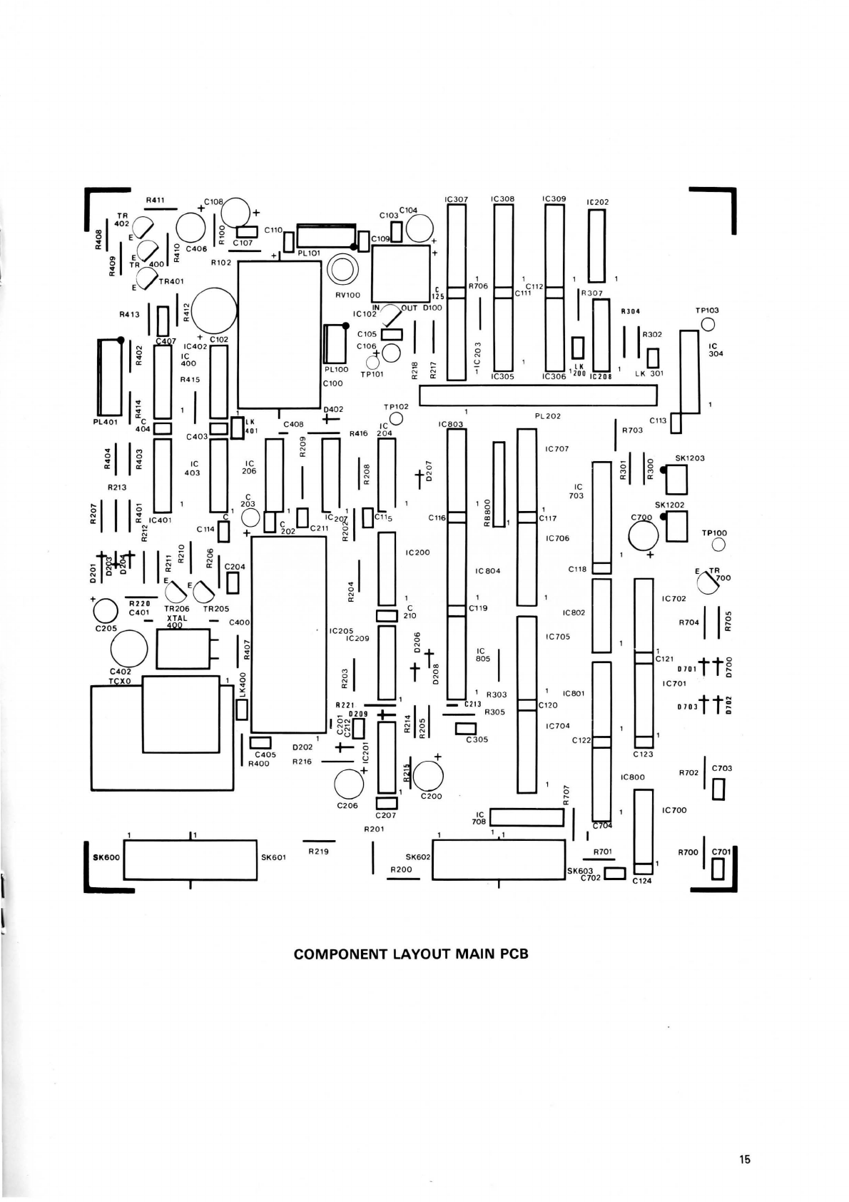
COMPONENT
LAYOUT
MAIN
PCB
15
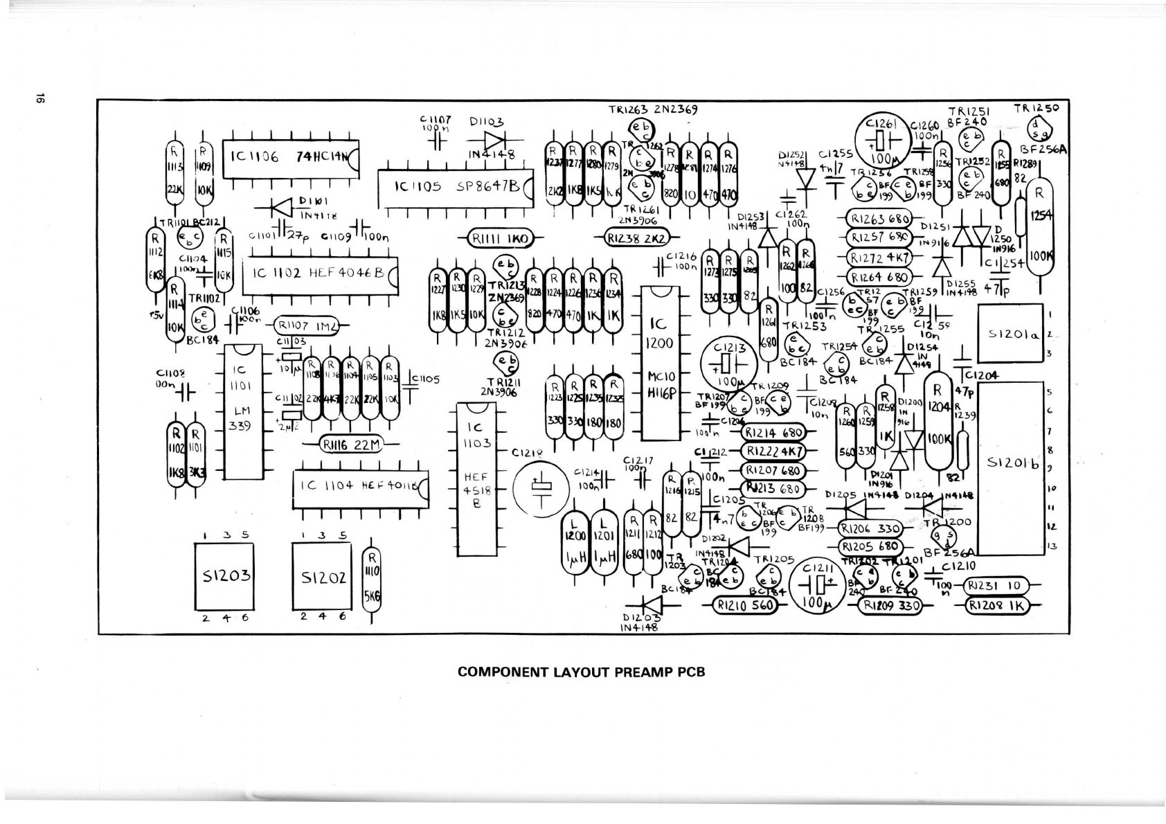
c.
1107
·~F
IC.
1105
IC
\1
02 H
E.F
40 4-6B
~1105
T
I
~
S I .3 .S
I
S11031
I
SILOl1
·~
2. "\" 6
2.
4 t,
DII0..3,
~
S
P%
47B
e.
b
TRZ
2 '
Rl21
N
~~
~
T
A.12I1
2N~'.'06
.......
-~
I
c.
\\0
~
H.12.E,3,
ZNBb~
@
C.12-1
'?
HEF
4 S l8
E,
~
~~
~jl--
T
ll.00
12.
I
1-\
I
COMPONENT
LAYOUT PREAMP PCB
g
I"
IL
.--------
-------------
--rc
r -
D
S'r
!!,
D~Y
7
\).'.,Y
S
~~
'D<oO,!i
D..,
u~
DS
O/
"~
© @ @ @
"''
'
,o
r,
~
I\ R
10
...
!>
IQ~
•-S
I$
IQ > "
0\
c
<ooo
..,
,
I.JO 7 7 7
...L
!i(
!)
T
1
00~
'"
51010
□
[g]
1\
11.N
(,,E
®000
00
@
~00000
G
°l>
L.G.
00
1"
PL
"OI
Components
shown
dotted are
ob
scured
by
higher components
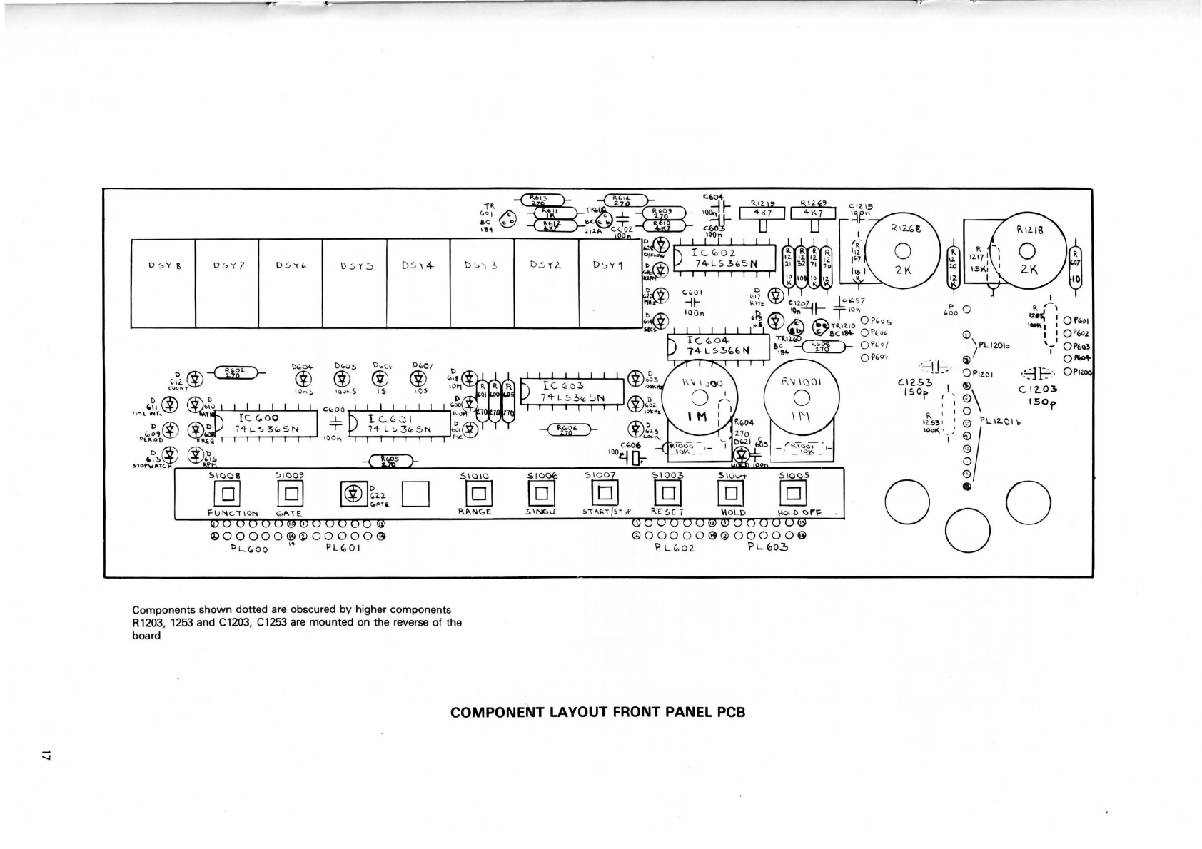
R1203, 1253 and C1203, C1253 are mounted on the reverse
of
the
board
r-'---'--'--'--'-----'-----'-~-~
-~:!,
Ic«o:!> W,-.
7'\-~S3c,,'..,
N
@
000
0 0 @
@0
0
000
@
? L
"oz.
PL.M~
COMPONENT
LAYOUT FRONT PANEL PCB
0PI
C\2.0J.
ISOf'

Df.27
"05S I OOl S IC) 0 I
Pb0
6
II
IIII
II
11111111
D R R
1251
[i]
12.0I
N>Z6
IM
61
Sl251
o
Pi201
5.120
I
11111111
I C
a'.
C
11111111
1252
1200
I
8p
220n
512.50
m
512..00
11111111
m
11111111
l!i
R\250
51
!ill
~
PL
1201
b
COMPONENT LAYOUT SUB BOARD
PCB
18
PGOlg
IPWl(Q)
~03
P,04 0
R
12.00
51
D
(il5
D~24
This manual suits for next models
4
Table of contents
Popular Cash Counter manuals by other brands

Carrera
Carrera Digital 124 Series Assembly and operating instructions

Hengstler
Hengstler signo 723.1 operating instructions

POL-EKO
POL-EKO LKB 2002 instruction manual

Precision Digital Corporation
Precision Digital Corporation PD6820 manual

CPI
CPI CUMMINS ALLISON CA-200 user guide

Leica Microsystems
Leica Microsystems DARKFIELD QUEBEC 3325 instruction manual

Cashmaster
Cashmaster Sigma 170 quick start guide

Royal Sovereign
Royal Sovereign RBC-1003 owner's manual

Nautilus Hyosung
Nautilus Hyosung MONiMAX5300SE System Operator's manual

Delfi
Delfi DELFI RENTAL quick guide

Lighthouse
Lighthouse ApexPortable Read me first

Royal Sovereign
Royal Sovereign RBC-ED250-CA owner's manual


