BLU Products Life Pure User manual

Page 1 of 22
BLU Life Pure Service Manual

Page 2 of 22
Contents
1. OUTLINE............................................................................................................... 3
1.1. Mobile Introduction ................................................................................................................................3
1.2. Motherboard Components Distribution................................................................................................5
2. SIGNAL FLOW AND FAULT ANALYSIS............................................................ 5
2.1. RF Part .....................................................................................................................................................5
2.1.1. Block Diagram of the RF Section .....................................................................................................5
2.1.2. Signal flow of the RF Transmitting Part ...........................................................................................6
2.1.2.1. Transmitting Path..............................................................................................................................6
2.1.2. Signal Flow of the RF Receiving Part...............................................................................................8
2.1.3.1. Receiving Path Components .........................................................................................................8
2.2. Baseband part........................................................................................................................................10
2.2.1 Block diagram of the Baseband part....................................................................................................10
2.2.2 Power Management............................................................................................................................. 11
2.2.3 Audio Section......................................................................................................................................12
2.2.3.1 Audio Codec Circuit ...................................................................................................................12
2.2.3.2 MIC& Receiver Loop .................................................................................................................13
2.2.3.3 Headset Loop ..............................................................................................................................14
2.2.4 Baseband Fault issues..........................................................................................................................15
2.2.4.1 Analysis of the keyboard fault ....................................................................................................16
2.2.4.2 Analysis of Display module circuit.............................................................................................17
2.2.4.3 FM Module .................................................................................................................................17
2.2.4.4 Camera Module...........................................................................................................................18
2.2.4.5 IO Interface.................................................................................................................................19
2.2.4.6 SIM Card Circuit.........................................................................................................................19
2.2.4.7 BT/WIFI/GPS Circuit .................................................................................................................20
2.2.4.8 G-sensor Circuit..........................................................................................................................20
2.2.4.9 M-sensor Circuit .....................................................................................................................21
2.2.4.10 Gyroscope Circuit...................................................................................................................22
Page 3 of 22
1. Outline
1.1. Mobile Introduction
Product Hardware Definition
Base Chip Set
BB
MT6589WTK
PMIC
MT6320
Transceiver
MT6167
Camera DSP/MMP
NA
RFPA
SKY77590
FM
MT6628
BT
MT6628
Audio
CODEC&PA
YD165C
Memory
Samsung KMI2U000MA-B800
TP IC
GT915
Peripheral
Configuration
LCD
5.0"
Backlight driver
LM3630
CAMERA
13million pixel
Memory card
NA
Antenna
monopole
Basic
Performance
Indicators
Leakage current
≤ 90uA
Standby current
≤ 7mA
Call current as
maximum power
TBD
Board-level power
GSM
32.5dBm
DCS
29.5dbm
Board-level receiver
sensitivity
GSM
-108dbm
DCS
-109dbm
TRP
GSM
27dbm
DCS
25dbm
Band1
23dbm
Band8
22dbm
TIS
GSM
-103dbm
DCS
-105dbm
Band1
-104dbm
Page 4 of 22
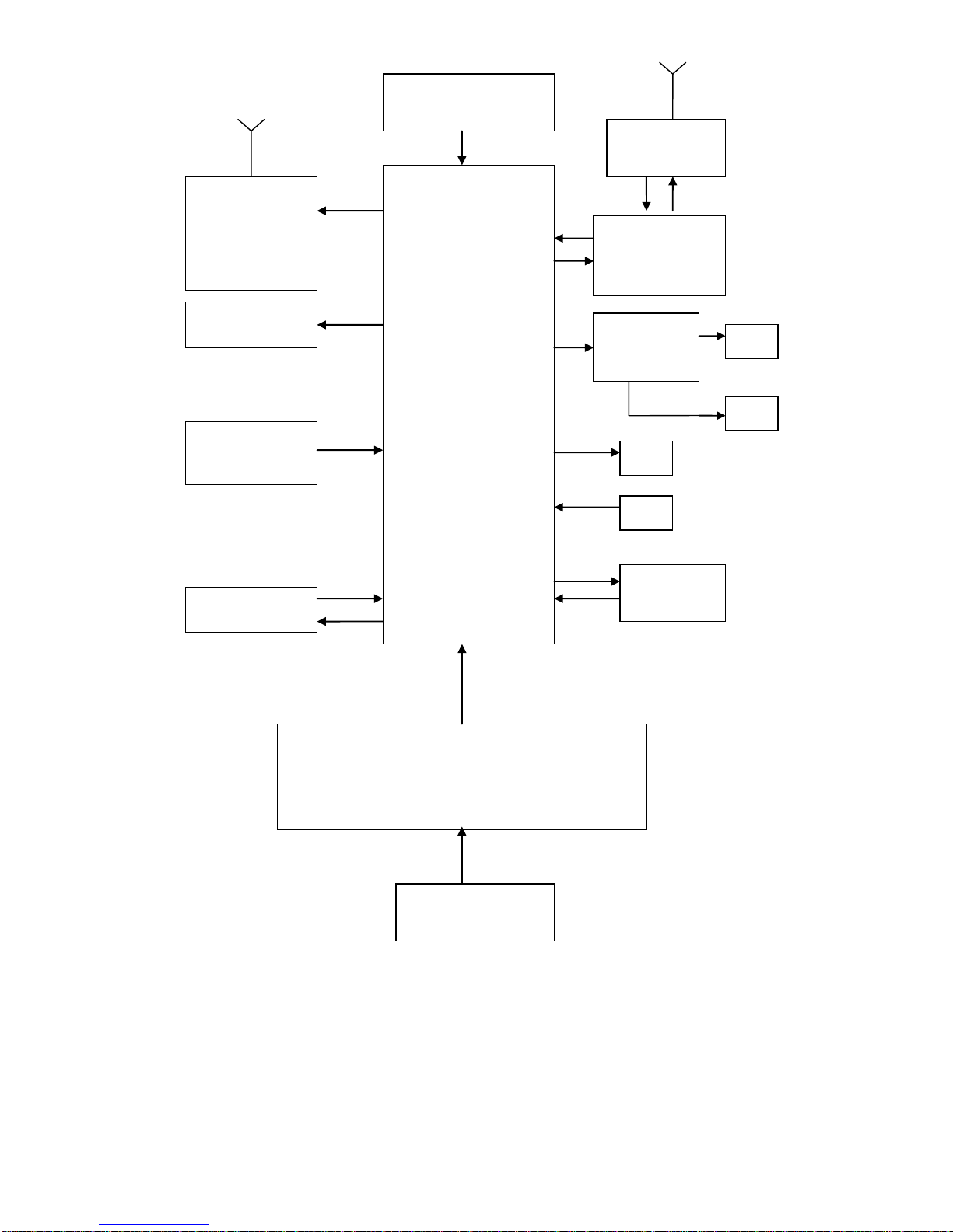
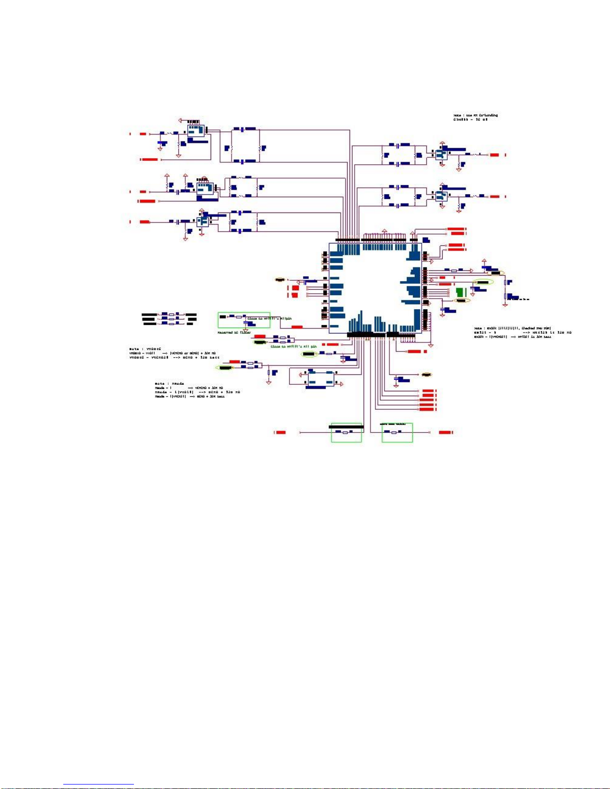
System Block Diagram
CPU
MT6589
PMIC
MT6320
BATTRY
CAMERA
FM、BT、
WiFi、GPS
LCD&CTP
KEYPAD
MEMORY
MT6167
SKY77590
YD165
SPK
HP
REC
single SIM
CARD
MIC
Page 5 of 22
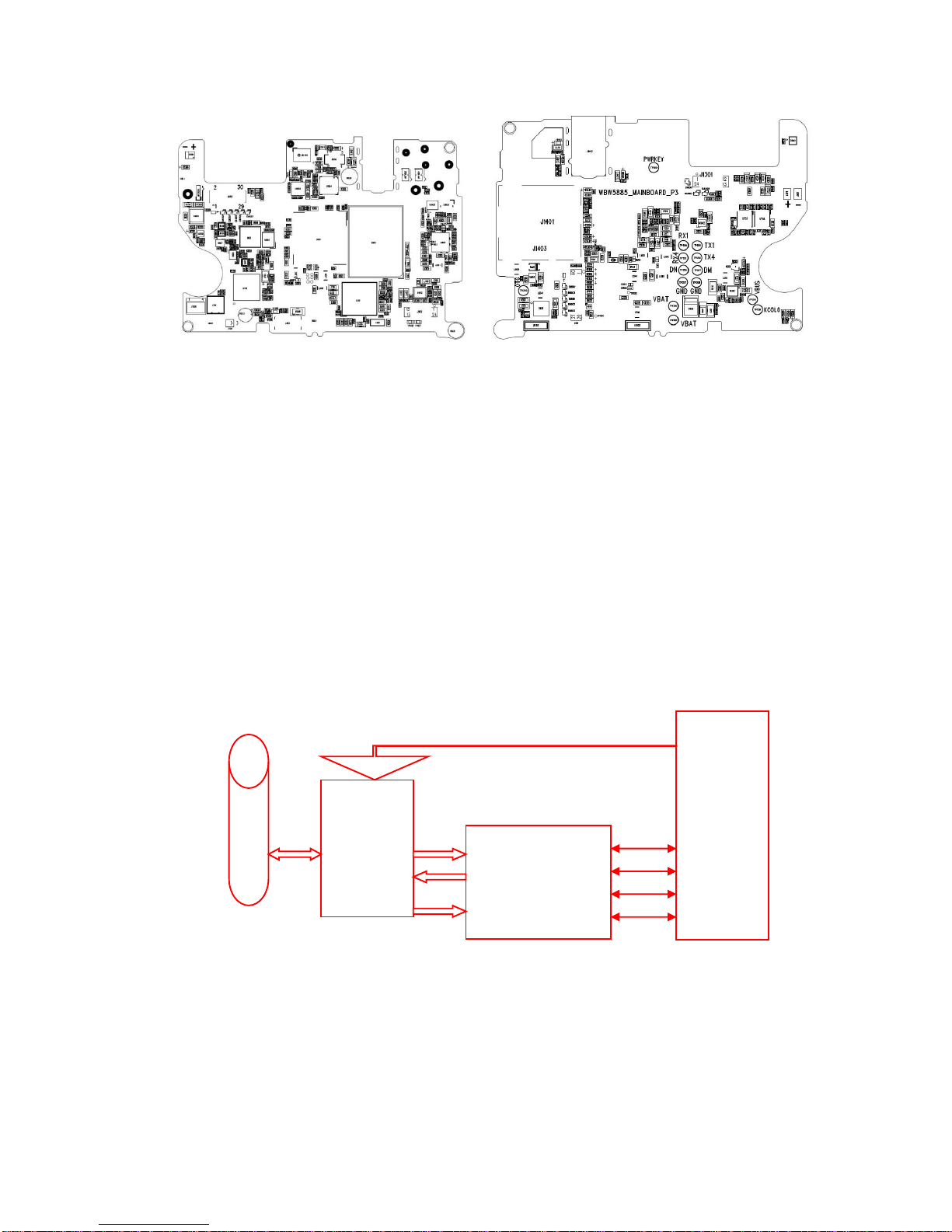
1.2. Motherboard Components Distribution
2. Signal Flow and Fault Analysis
2.1. RF Part
2.1.1. Block Diagram of the RF Section
RF Block Diagram
A
N
T
PA &
Ant Switch
SKY7759
0
Transceiver
MT6167
CPU
MT6589
GGG
Page 6 of 22
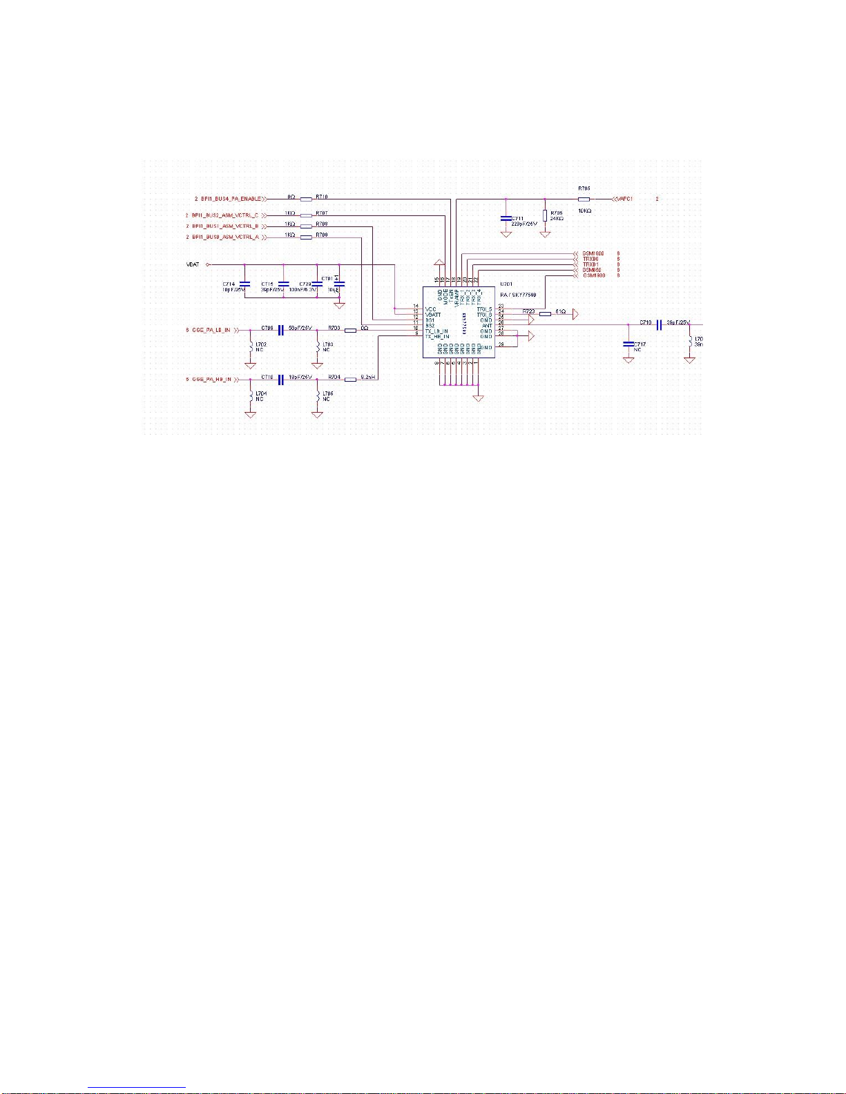
2.1.2.Signal flow of the RF Transmitting Part
2.1.2.1. Transmitting Path
Page 7 of 22
Maintenance Flow Chart of the Transmitting Issue:
(NO launch)Connect the PC and the phone with maintenance line,
then making the phone into the RF state with META software
Check Transceiver to see
if IQ signals exist.
`
Check the PA output to
see if there is RF signal in
the path.
Y
Check CPU
N
Check RF coaxial
switch or matching
network.
Y
Check the Transceiver
to see if there is RF
signal output.
N
VBAT,PA_EN,BAN
DSW_DCS,VAPC
是否 OK?
Replace PA
Y
Check CPU
Y
Check Transceiver if LE、
SCLK/SDAT、
RFVCOEN、VCXOEN
have the correct signal.
N
N
N
N
Y
Replace Transceiver
Page 8 of 22
2.1.2. Signal Flow of the RF Receiving Part
2.1.3.1. Receiving Path Components
Receiving path is shown in the following figure:
Page 9 of 22
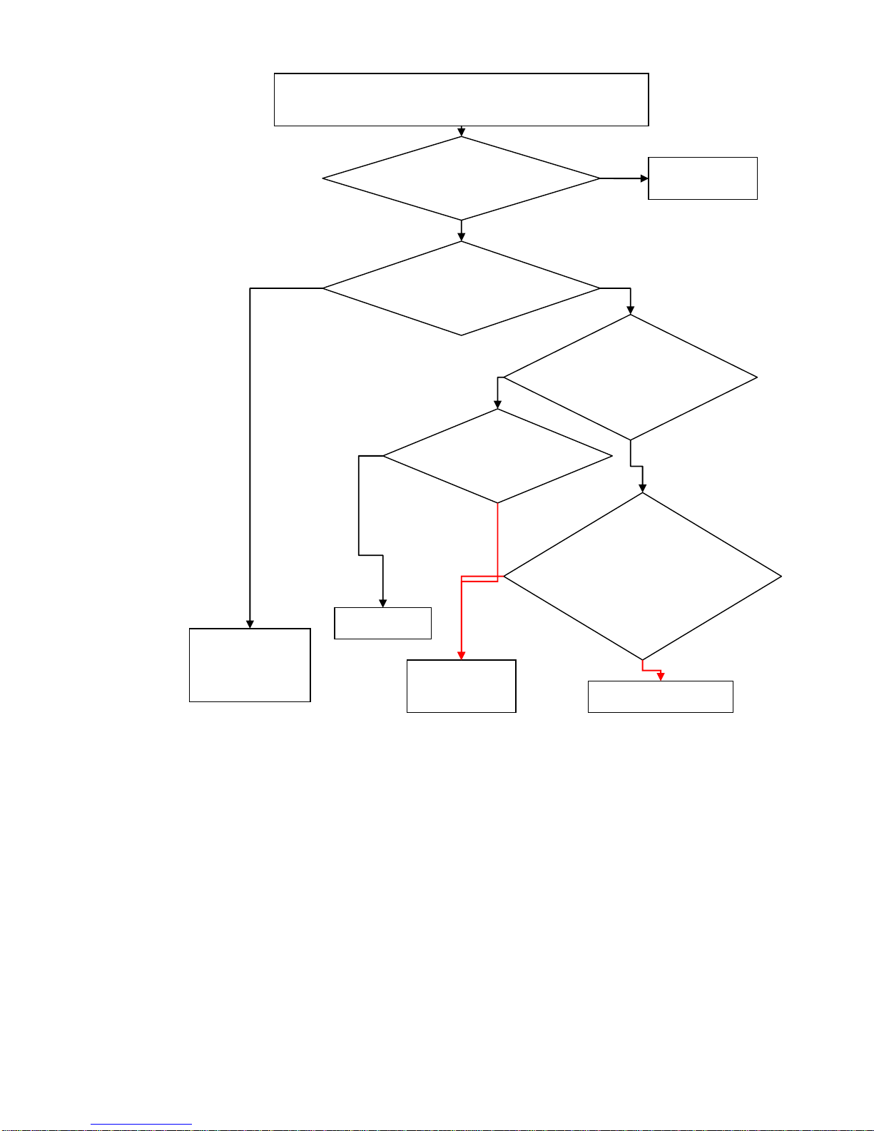
Maintenance flow chart of the receiving Issues:
No receiving
Start the META software to connect the PC and the phone,making the phone into the
receiving state. Signal generator is also adjusted to the correspond CH.And signal lines
connected to the phone.
的同轴开关上。
Transceiver has
IQ?
Check
CPU
Y
Transceiver has
received signal?
号?
N
Transceiver SDATA、
SCLK、LE、CXOEN
are correct ?
Y
Check
CPU
N
Whether the
voltage of the
transceiver is
normal? Whether
26MHZ is
normal?
正常?
Y
Check the
corresponding
power supply and
26MHZ resulting
circuit
N
Replace transceiver
Y
PA has
received
signal?
N
Check to see if there has
signal in the matching
circuit between PA and
ANT
N
Check to see if there
has signal in the
matching circuit
between PA and
transceiver
Y

Page 10 of 22
2.2. Baseband part
2.2.1 Block diagram of the Baseband part
CPU
MT6589
PMIC
MT6320
BATTRY
CAMERA
FM、BT、
WiFi、GPS
LCD&CTP
KEYPAD
MEMORY
MT6167
SKY77590
YD165
SPK
HP
REC
SINGLE
SIM CARD
MIC
Page 11 of 22
2.2.2 Power Management
The power management module is PMU IC:MT6320.
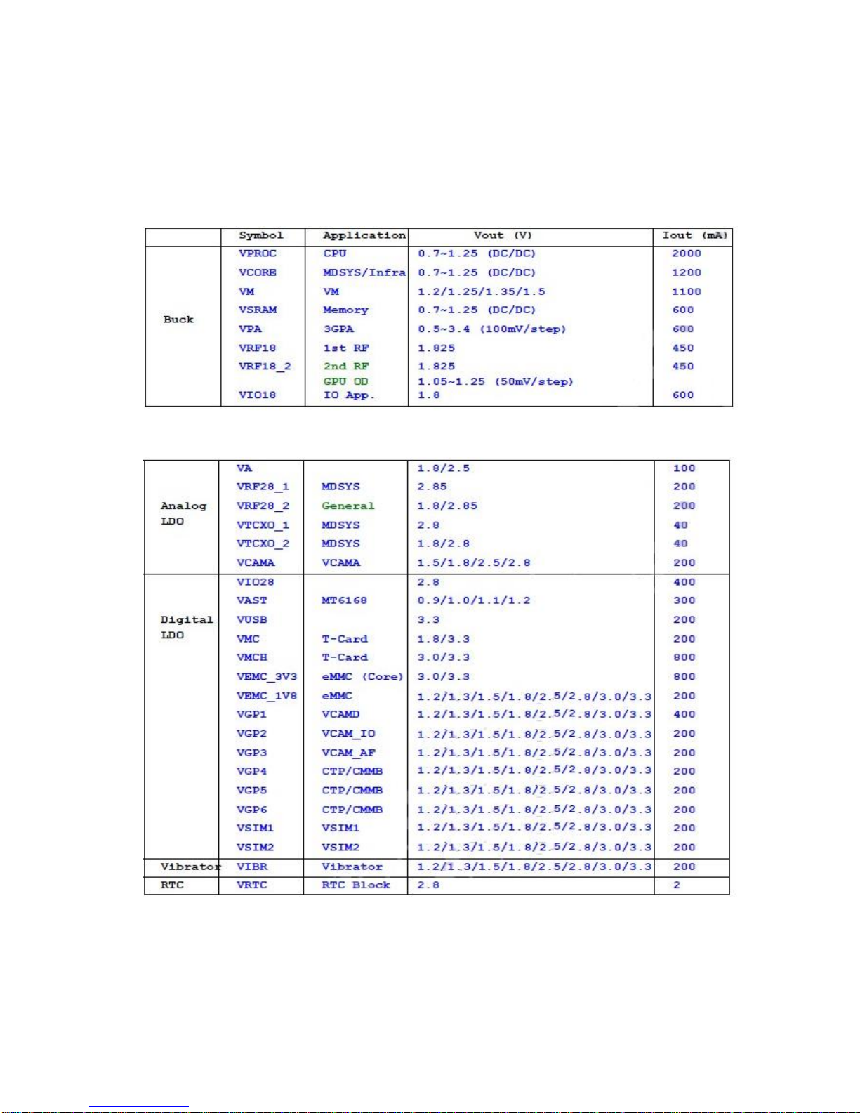
2.2.2.1 Mobile power supply system
DC-DC:
LDO:

Page 12 of 22
2.2.3 Audio Section
2.2.3.1 Audio Codec Circuit
This phone applies YD165 which is a class D and non-crack noise YAMAHA amplifier to drive speaker.
Block diagram of the audio system is as below:

Page 13 of 22
2.2.3.2 MIC& Receiver Loop
MIC Audio path is shown below:MIC must have a bias voltage in order to operate normally——2.0±
0.1V. When MIC is in good condition but loop MIC has no echo, then you need to check the basic bias
voltage signal of the MICBIASP and MICBIASSP, the language signals of the RECEIVER and MIC also
need to be checked.
Receiver loop is simple. The output of BB drive Receiver directly through Filter and ESD protected
network, as shown below:

Page 14 of 22
2.2.3.3 Headset Loop
Headset loop includes two signals: Headset speaker and MIC,If the headset fitting were in good condition,
when the headset plug in, it appears abnormal, such as: The Headset speaker has no sound、the MIC is
invalid. All this need to check the access conditions of the circuit above.
Page 15 of 22
2.2.4 Baseband Fault issues
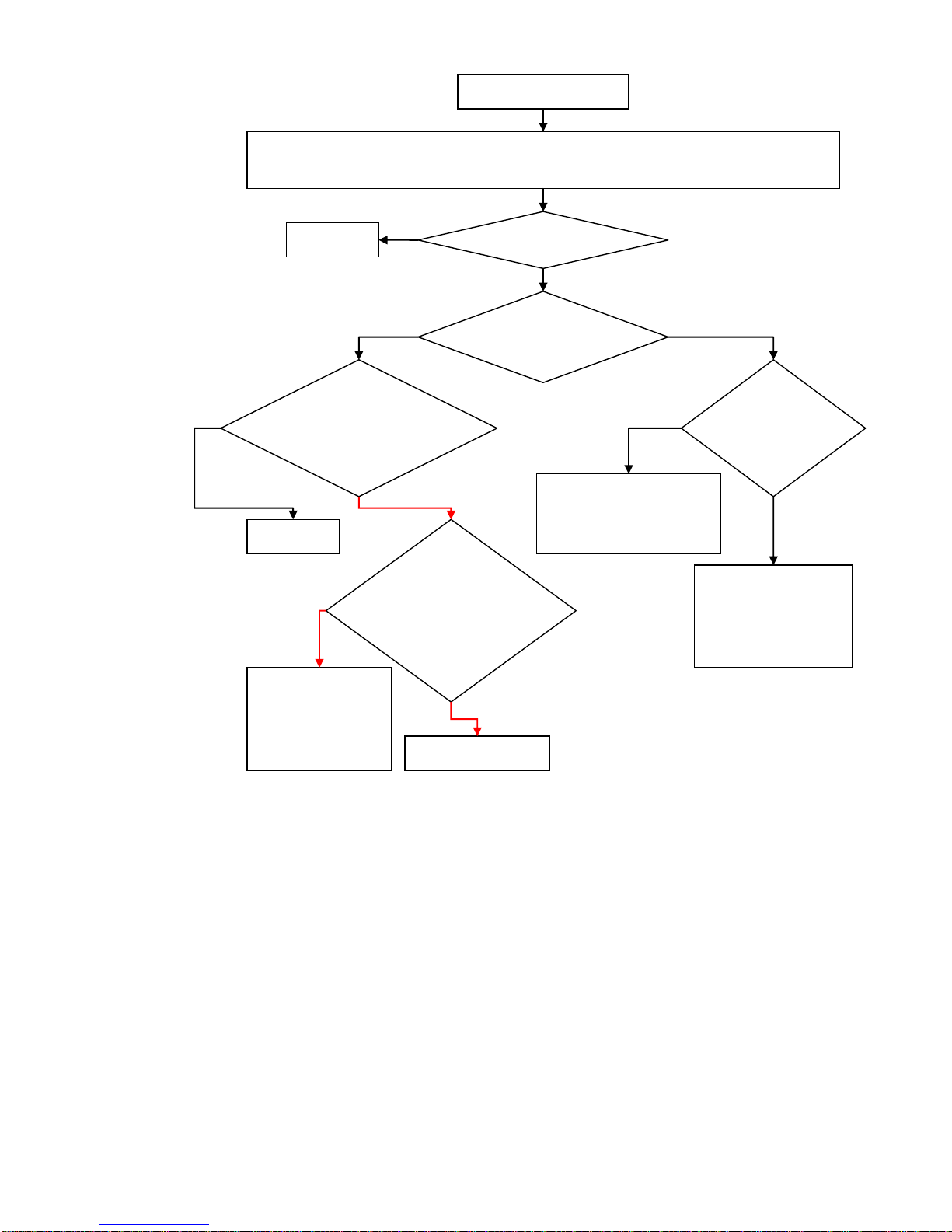
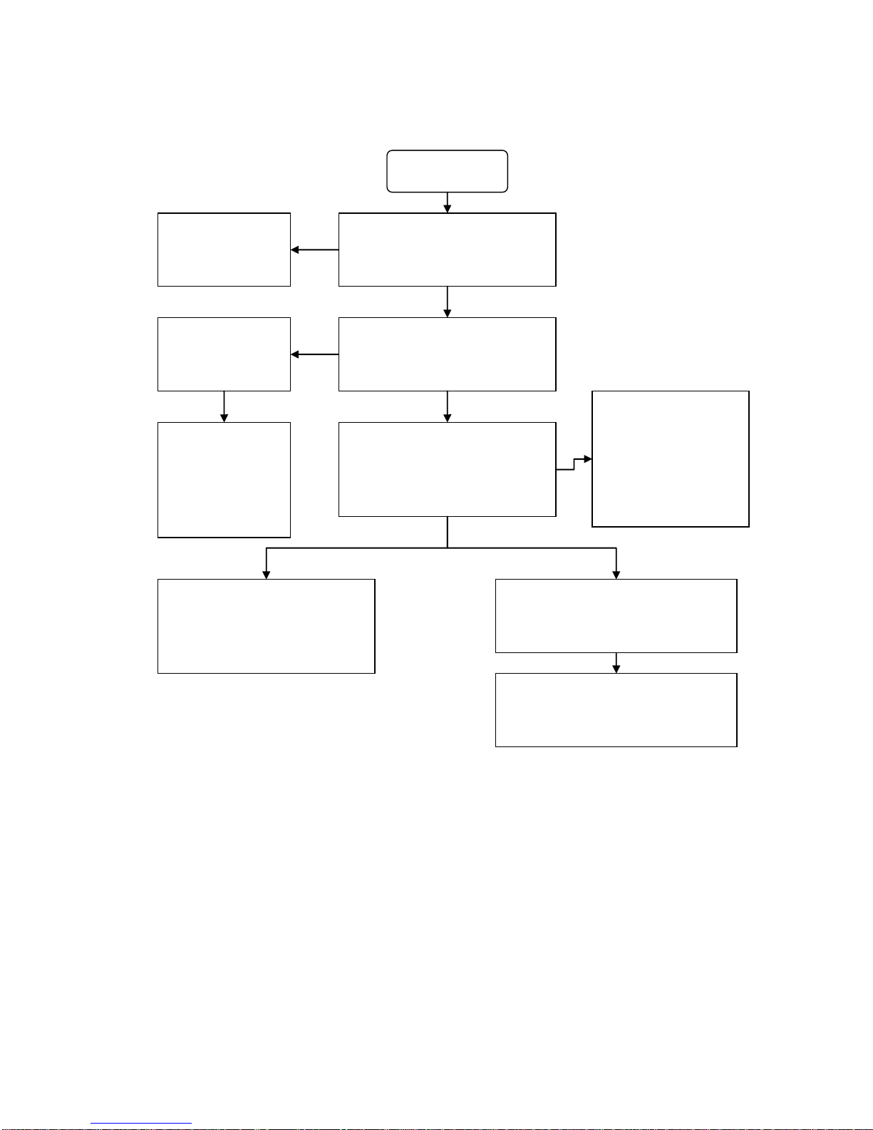
Maintenance process of the download failure Issues:
Download Fail
Check to see if it is caused by other
factors such as: configuration, download
cable, power supply, software and PC
Exclude the reason of
download failure
caused by other factors
Yes
Check to see if the serial ports between
pc and cell phone is smooth
Check if the system
connector is poor
soldered or damaged.
NO
NO
Check the resistance,
capacitance and the
EDC devices between
the system connector
and the CPU.
NO
Connect the download cable then
observe the Ammeter to see if it
shows high current(The normal
current generally about 30mA)
Yes
Quickly disconnect the
connection, and gently
touch the chip to see if it is
hot. If not, then focus point
using the multi-meter to
measure the short circuit.
Yes
Check the power manager and open the
LDO to see if the voltage supply is
normal and whether there is power
supply circuit open.
Little or no current
Check VCORE、VDD、VADD、VTCXO、
VRTC、VMEM、Measure the clock signal of
26MHZ、32KHZ.
Current normal but download fail
Check CPU and NAND FLASH、SDRAM to
see if they are OK and the LDO is normal.
Page 16 of 22
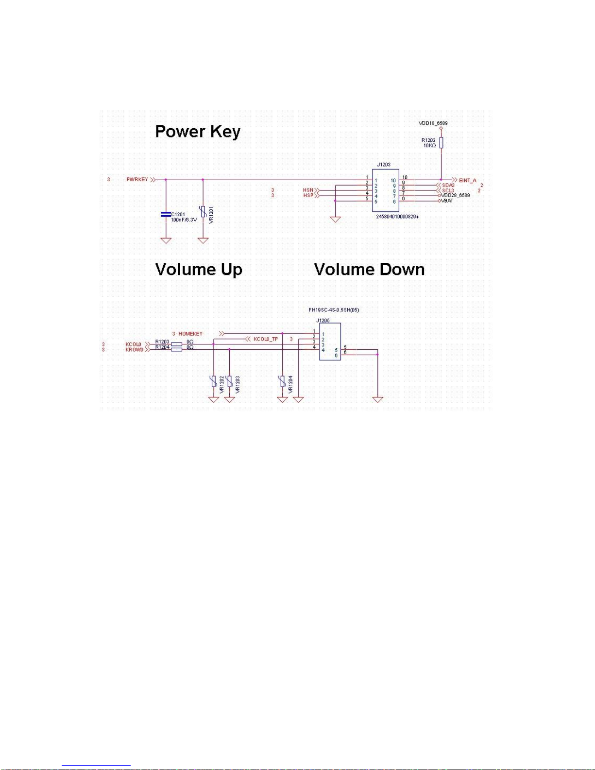
2.2.4.1 Analysis of the keyboard fault
This handset has 3 side keys. All the keyboard circuits use the scanning method to detect
except the power button .When a button is pressed the scanning signal will be triggered, then
the corresponding row and column will be detected. The function of the key can be identified
according to software definition.
a. The cell phone can power on ,but all the keys are invalid.
In general, this situation is caused by some key short-circuit, the equivalent of a
long pressing this button.
At this point ,you should analyze the following first:
⑴Check the connector external exclusion and varistor to see if they short-circuit.
⑵Then ,check the connector to see whether it is short-circuit when it is welded.
b. Failure of a single button
This situation needs to check whether the beneath of the DOME key is dirty. If the
problem still exists, you have to check whether the circuit is open.
c. Failure of a few buttons
This situation is usually caused by a short-circuit row or column. Checking the
interface circuit to see if it has open weld phenomena and detect the
disconnected phenomena of the resistance.
Page 17 of 22
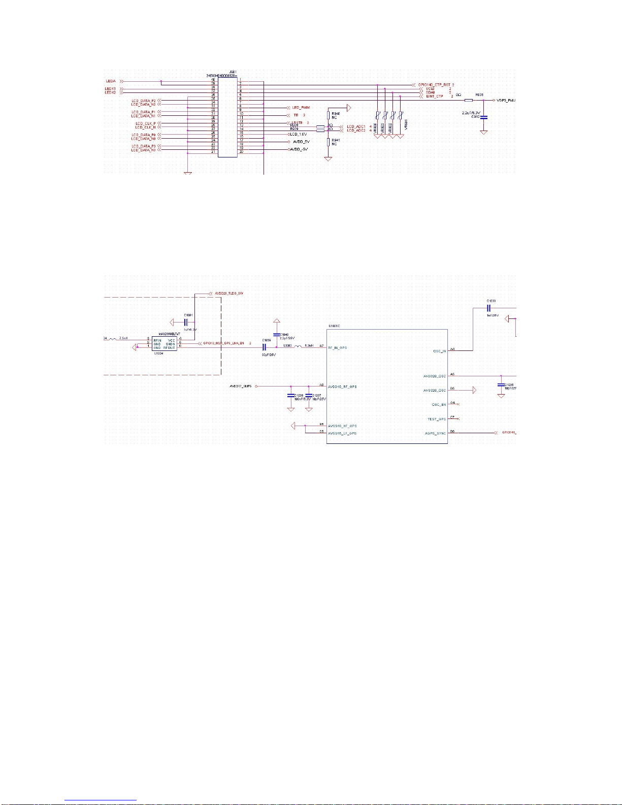
2.2.4.2 Analysis of Display module circuit
Display module use the 5.0"FHD LCD.
2.2.4.3 FM Module
FM adopts the design of MT 6628.
Page 18 of 22
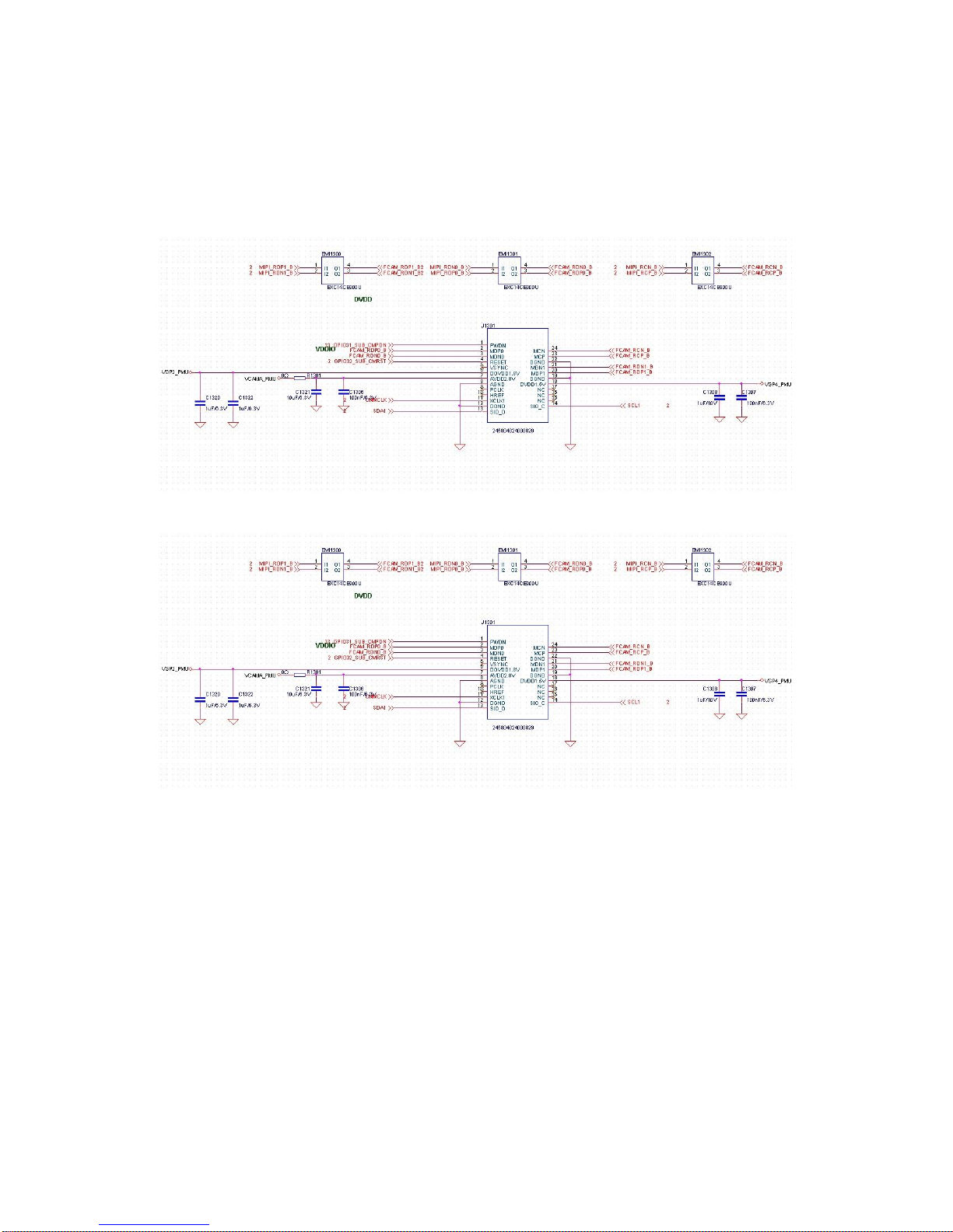
2.2.4.4 Camera Module
This module uses the 5million pixel front camera and 13 million pixel rear camera,
connecting to baseband chip through connector. The welding of the connector is the main
reason for the camera malfunction.
Camera Interface Circuit:
5million pixel front camera
13 million pixel rear camera
Power supply circuit : VGP2_PMU _1.8V for camera I/O port, VGP1_PMU 提供 1.5V for
camera core, VCAMA_PMU _2.8V for analog power.
Page 19 of 22
2.2.4.5 IO Interface
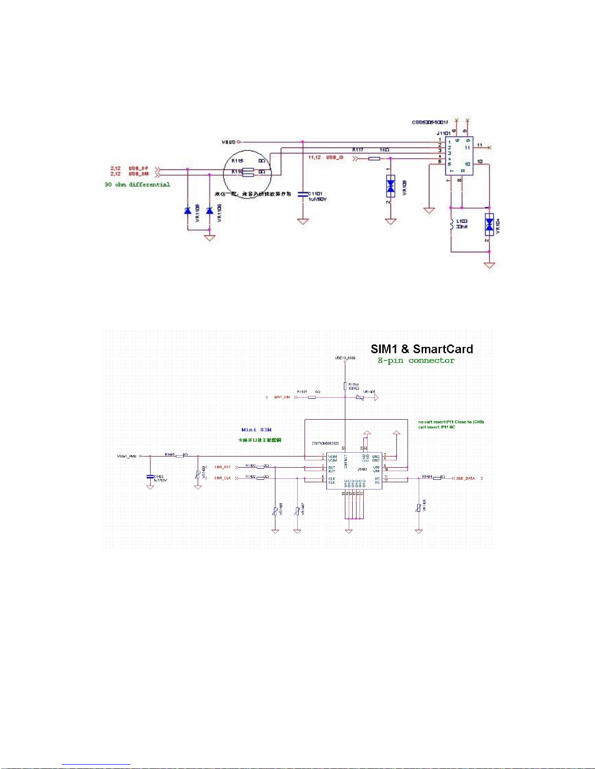
IO applies 5pin standard interface,which realize the functions of USB, charging and
download.
2.2.4.6 SIM Card Circuit
Switch of dual SIM cards is integrated into baseband.
SIM Card Tray
Page 20 of 22
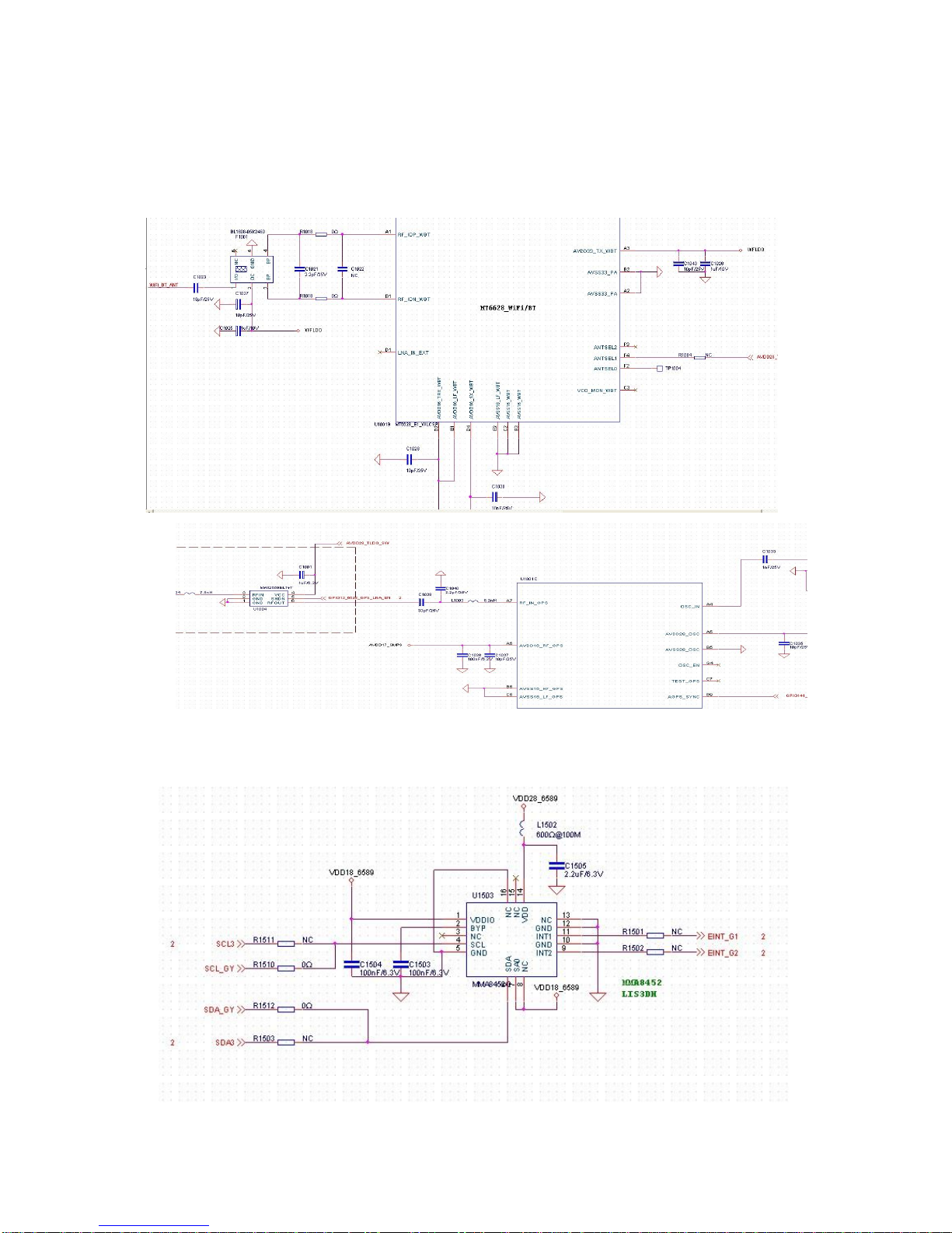
2.2.4.7 BT/WIFI/GPS Circuit
BT/WiFi/GPS are integrated into MT6628.
2.2.4.8 G-sensor Circuit
Table of contents
Other BLU Products Cell Phone manuals

BLU Products
BLU Products Jenny User manual

BLU Products
BLU Products NEO JR User manual

BLU Products
BLU Products G63 User manual

BLU Products
BLU Products G33 User manual

BLU Products
BLU Products J10L User manual

BLU Products
BLU Products BLU DASH User manual

BLU Products
BLU Products VIEW 1 User manual

BLU Products
BLU Products BLU VIVO IV User manual

BLU Products
BLU Products G93 User manual

BLU Products
BLU Products JOY FLEX User manual


