CMOSTEK CMT2300A-EQR User manual

CMT2300A
Rev1.0a | 1/50
www.cmostek.com
Features
Frequency range: 127 ~1020 MHz
Modem: OOK, (G)FSK and (G)MSK
Data rate: 0.5 ~ 300 kbps
Sensitivity:
- 121 dBm 2.0 kbps, FRF = 433.92 MHz
-111 dBm 50 kbps, FRF = 433.92 MHz
Voltage range: 1.8 ~3.6 V
Transmit current: 23 mA @ 13 dBm, 433.92 MHz, FSK
72 mA@ 20 dBm, 433.92 MHz, FSK
Rx current:
8.5 mA @ 433.92 MHz, FSK (High power mode)
7.2 mA @ 433.92 MHz, FSK (Low power mode)
Super-low Power receive mode
Sleep current: 300 nA, Duty Cycle = OFF
800 nA, Duty Cycle = ON
Receiver features:
Fast and stable automatic frequency control (AFC)
3 types of clock data recovery system (CDR)
Fast and accurate signal detection (PJD)
4-wire SPI interface
Direct and packet mode supported
Configurable packet handler and 64-Byte FIFO.
NRZ, Manchester codec, Whitening codec, Forward
Error Correction (FEC)
Description
CMT2300Ais an ultra-low power, high performance, OOK (G)
FSK RF transceiver suitable for a variety of 140 to 1020 MHz
wireless applications. It is part of the CMOSTEK
NextGenRFTM RF product line. The product line contains the
complete transmitters, receivers and transceivers. The high
integration of CMT2300A simplifies the peripheral materials
required in the system design. Up to +20 dBmTx Power and
-121 dBm sensitivity optimize the performance of the
application. It supports a variety of packet formats and codec
methods to meet the needs of various different applications.
In addition, CMT2300A also supports 64-byte Tx/Rx
FIFO, GPIO and interrupt configuration, Duty-Cycle
operation mode, channel sensing, high-precision RSSI,
low-voltage detection, power-on reset, low frequency clock
output, manual fast frequency hopping, squelch and etc. The
features make the application design more flexible and
differentiated. CMT2300A operates from 1.8 V to 3.6 V. Only
8.5 mAcurrent is consumed when the sensitivity is -121 dBm,
SuperLow Power mode can further reduce the chip power
consumption. Only 23mA Tx current is consumed when the
output power is 13 dBm.
Application
Automatic meter reading
Home security and building automation
ISM band data communication
Industrial monitoring and control
Remote control and security system
Remote key entry
Wireless sensor node
Tag reader
Ordering Information
Model
Frequency
Package
MOQ
CMT2300A-EQR
433.92 MHz
QFN16
3,000 pcs
Please see Table 23 for more ordering details.
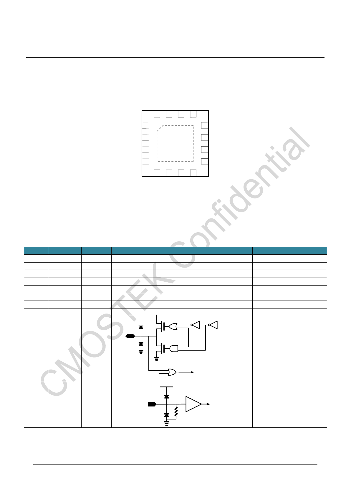
QFN16 (3X3) Packaging
17
GND
SCLK
SDIO
CSB
FCSB
XI
XO
GPIO2
GPIO1
AVDD
PA
RFIN
RFIP
GPIO3
DVDD
DGND
AGND
13
14
15
16
1
2
3
4
5678
9
10
11
12
CMT2300 Top View
CMT2300A
Ultra-low Power Sub-1GHz RF Transceiver
SoC

CMT2300A
Rev1.0a | 2/50
www.cmostek.com
Table of Contents
1. Electrical Characteristics ....................................................................................................................4
1.1 RecommendedOperation Condition...................................................................................................................4
1.2 Absolute Maximum Rating..................................................................................................................................4
1.3 PowerConsumption ...........................................................................................................................................5
1.4 Receiver.............................................................................................................................................................6
1.5 Transmitter.........................................................................................................................................................8
1.6 Settling Time ......................................................................................................................................................8
1.7 Frequency Synthesizer.......................................................................................................................................9
1.8 Crystal Oscillator .............................................................................................................................................. 10
1.9 Low Frequency Oscillator.................................................................................................................................10
1.10 Low Battery Detection......................................................................................................................................11
1.11 Digital Interface ................................................................................................................................................11
1.12 Figures of Critical Parameters.......................................................................................................................... 11
1.12.1 Rx Current VS. Supply Voltage................................................................................................................. 11
1.12.2 Rx Current VS. Voltage Temperature.......................................................................................................12
1.12.3 Sensitivity VS. Voltage.............................................................................................................................12
1.12.4 Sensitivity VS. Temperature.....................................................................................................................13
1.12.5 Tx Power VS. Supply Voltage..................................................................................................................14
1.12.6 Tx Phase Noise........................................................................................................................................14
2. Pin Descriptions.................................................................................................................................16
3. Typical Application Schematic..........................................................................................................18
3.1 Direct Tie Schematic Diagram.......................................................................................................................... 18
3.2 RF Switch Type Schematic .............................................................................................................................. 20
4. Function Descriptions .......................................................................................................................23
4.1 Transmitter....................................................................................................................................................... 24
4.2 Receiver...........................................................................................................................................................24
4.3 Additional Functions.........................................................................................................................................24
4.3.1 Power-On Reset (POR)...........................................................................................................................24
4.3.2 Crystal Oscillator......................................................................................................................................25
4.3.3 Sleep Timer..............................................................................................................................................26
4.3.4 Low Battery Detection..............................................................................................................................26
4.3.5 Received Signal Strength Indicator(RSSI)...............................................................................................26
4.3.6 Phase Jump Detector(PJD).................................................................................................................27
4.3.7 Automatic Frequency Control (AFC)........................................................................................................27
4.3.8 Clock Data Recovery (CDR)....................................................................................................................28
4.3.9 Fast Frequency Hopping..........................................................................................................................28
5. Chip Operation....................................................................................................................................29
5.1 SPI Interface..................................................................................................................................................... 29
5.2 FIFO.................................................................................................................................................................30
5.2.1 FIFO Read Operation ..............................................................................................................................31
5.2.2 FIFO Associated Interrupt........................................................................................................................32

CMT2300A
Rev1.0a | 3/50
www.cmostek.com
5.3 Operation State, Timing and Power Consumption ...........................................................................................33
5.3.1 Startup Timing..........................................................................................................................................33
5.3.2 Operation State........................................................................................................................................34
5.4 GPIO and Interrupt...........................................................................................................................................36
6. Packet Handler....................................................................................................................................39
6.1 Direct Mode...................................................................................................................................................... 39
6.2 Packet Mode .................................................................................................................................................... 40
7. Low Power Operation ........................................................................................................................42
7.1 Duty Cycle Operation Mode ............................................................................................................................. 42
7.2 Super-low Power Rx Mode............................................................................................................................... 42
7.3 Receiver “Power VS Performance” Configuration ............................................................................................ 43
8. User Register......................................................................................................................................44
9. Ordering Information .........................................................................................................................46
10. Packaging Information .....................................................................................................................47
11. Top Marking.......................................................................................................................................48
12. Revise History ...................................................................................................................................49
13. Contacts.............................................................................................................................................50
CMT2300A
Rev1.0a | 4/50
www.cmostek.com
1.Electrical Characteristics
VDD= 3.3 V, TOP= 25 °C, FRF = 433.92 MHz, the sensitivity is measured by receiving a PN9 coded data and
matching the impedance to 50Ω under the 0.1%BER standard. Unless otherwise stated, all results are tested on
the CMT2300A-EM evaluation board.
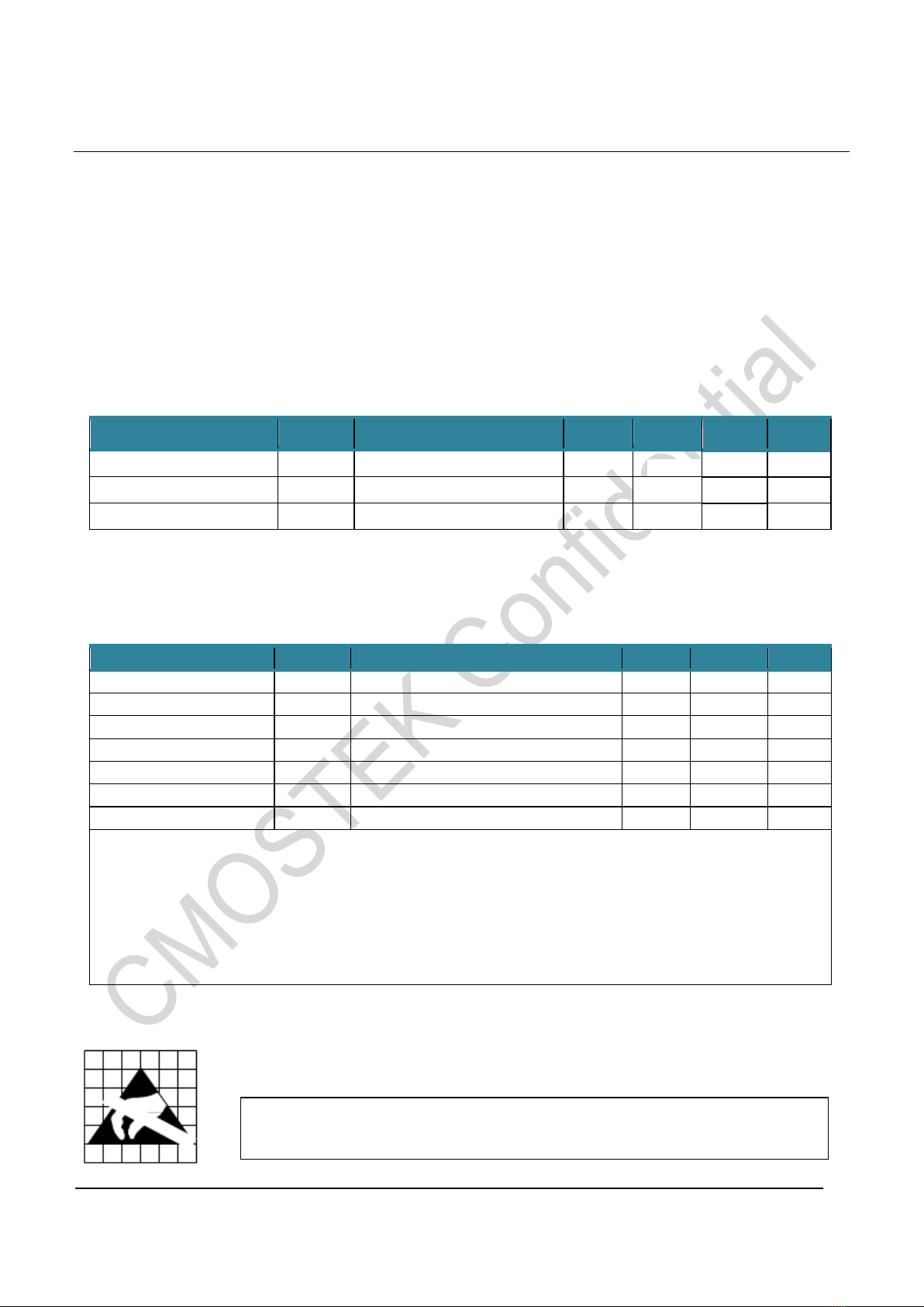
1.1 Recommended Operation Condition
Table 1. Recommended Operation Conditions
Parameter
Symbol
Condition
Min.
Typ.
Max.
Unit
Power voltage
VDD
1.8
3.6
V
Operating temperature
TOP
-40
85
℃
Power voltage slope
1
mV/us
1.2 Absolute Maximum Rating
Table 2. Absolute Maximum Ratings[1]
Parameter
Symbol
Conditions
Min
Max
Unit
Supply Voltage
VDD
-0.3
3.6
V
Interface Voltage
VIN
-0.3
VDD +0.3
V
Junction Temperature
TJ
-40
125
℃
Storage Temperature
TSTG
-50
150
℃
Soldering Temperature
TSDR
Lasts at least 30 seconds
255
℃
ESD Rating[2]
Human Body Model (HBM)
-2
2
kV
Latch-up Current
@ 85 ℃
-100
100
mA
Notes:
[1]. Exceeding the Absolute Maximum Ratings may cause permanent damage to the equipment. This value is a pressure
rating and does not imply that the function of the equipment is affected under this pressure condition, but if it is exposed
to absolute maximum ratings for extended periods of time, it may affect equipment reliability.
[2]. The CMT2300A is a high performance RF integrated circuit. The operation and assembly of this chip should only be
performed on a workbench with good ESD protection.
[2].
Caution! ESD sensitive device. Precaution should be used when handling the device in order
to prevent permanent damage.
CMT2300A
Rev1.0a | 5/50
www.cmostek.com
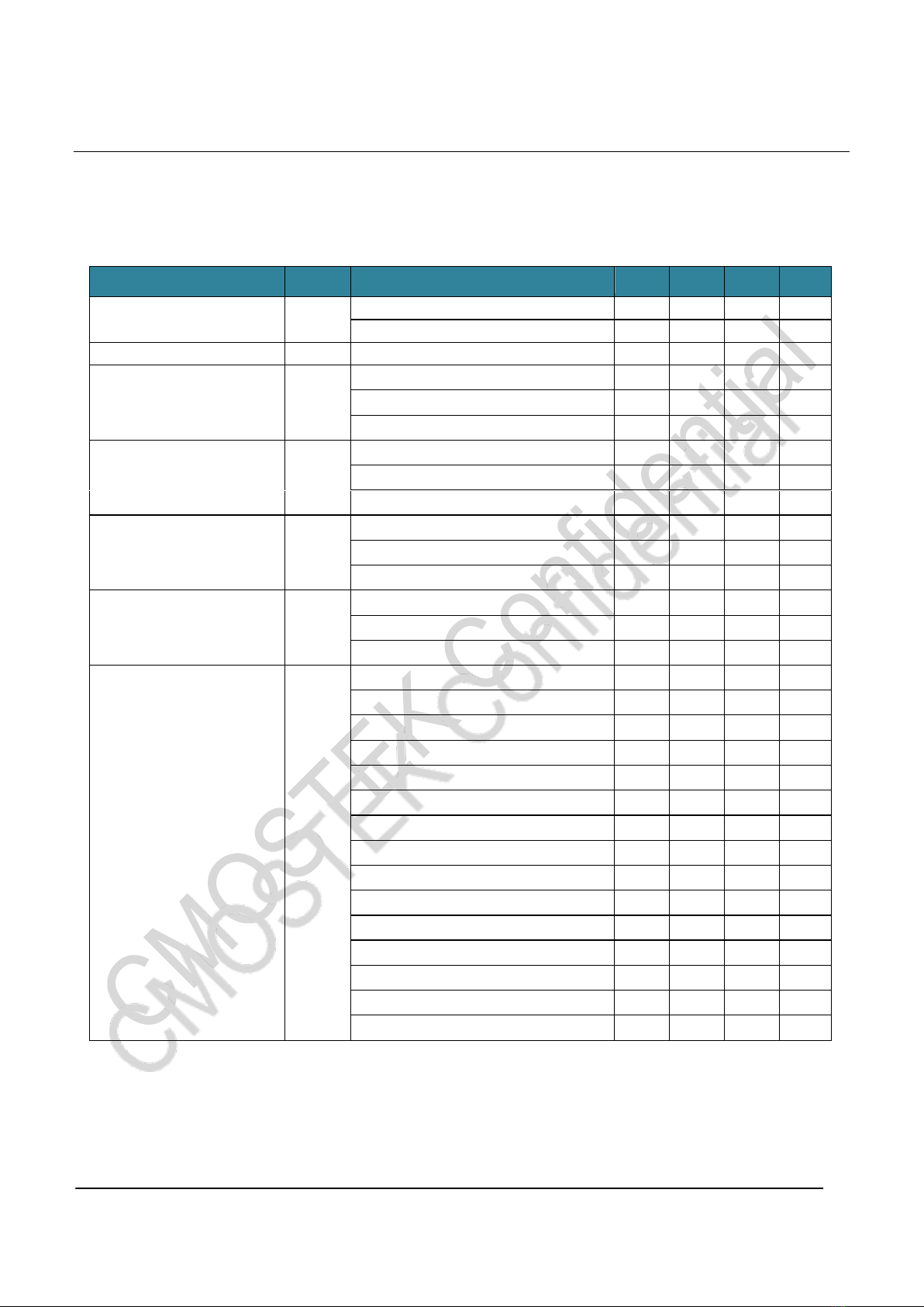
1.3 Power Consumption
Table 3. Power Consumption Specification
Parameter
Symbol
Condition
Min.
Typ.
Max.
Unit
Sleep current
ISLEEP
Sleep mode, sleep timer is off
300
nA
Sleep mode, sleep timer is on
800
nA
Standby current
IStandby
Crystal oscillator is on
1.45
mA
RFS current
IRFS
433 MHz
5.7
mA
868 MHz
5.8
mA
915 MHz
5.8
mA
TFS current
ITFS
433 MHz
5.6
mA
868 MHz
5.9
mA
915 MHz
5.9
mA
RXcurrent (high power mode)
IRx-HP
FSK, 433 MHz, 10 kbps,10 kHz FDEV
8.5
mA
FSK, 868 MHz, 10 kbps, 10 kHz FDEV
8.6
mA
FSK, 915 MHz, 10 kbps,10 kHz FDEV
8.9
mA
RX current (low power mode)
IRx-LP
FSK, 433 MHz, 10 kbps, 10 kHz FDEV
7.2
mA
FSK, 868 MHz, 10 kbps, 10 kHz FDEV
7.3
mA
FSK, 915 MHz, 10 kbps, 10 kHz FDEV
7.6
mA
TX current
ITx
FSK, 433 MHz, +20 dBm (Direct Tie)
72
mA
FSK, 433 MHz, +20 dBm (RF switch)
77
mA
FSK, 433 MHz, +13 dBm (Direct Tie)
23
mA
FSK, 433 MHz, +10 dBm (Direct Tie)
18
mA
FSK, 433 MHz, -10 dBm(Direct Tie)
8
mA
FSK, 868 MHz, +20 dBm(Direct Tie)
87
mA
FSK, 868 MHz, +20 dBm(RF switch)
80
mA
FSK, 868 MHz, +13 dBm (Direct Tie)
27
mA
FSK, 868 MHz, +10 dBm (Direct Tie)
19
mA
FSK, 868 MHz, -10 dBm (Direct Tie)
8
mA
FSK, 915 MHz, +20 dBm (Direct Tie)
70
mA
FSK, 915 MHz, +20 dBm (RF switch)
75
mA
FSK, 915 MHz, +13 dBm (Direct Tie)
28
mA
FSK, 915 MHz, +10 dBm (Direct Tie)
19
mA
FSK, 915 MHz, -10 dBm (Direct Tie)
8
mA

CMT2300A
Rev1.0a | 6/50
www.cmostek.com
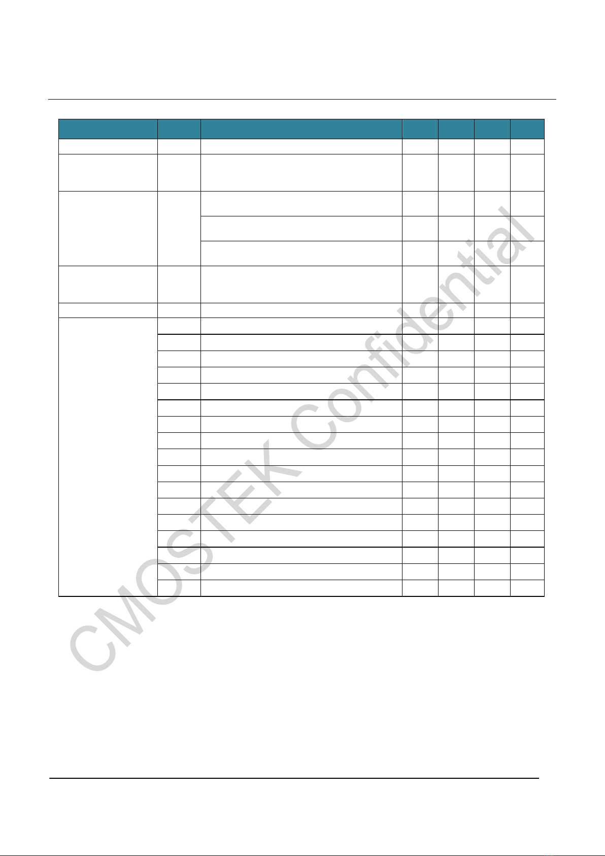
1.4 Receiver
Table 4. Receiver specification
Parameter
Symbol
Condition
Min.
Typ.
Max.
Unit
Data rate
DR
OOK
0.5
40
kbps
FSK and GFSK
0.5
300
kbps
Deviation
FDEV
FSK and GFSK
2
200
kHz
Sensitivity
@ 433 MHz
S433-HP
DR = 2.0 kbps, FDEV = 10 kHz
-121
dBm
DR = 10 kbps, FDEV = 10 kHz
-116
dBm
DR = 10 kbps, FDEV = 10 kHz(Low power setting)
-115
dBm
DR = 20 kbps, FDEV = 20 kHz
-113
dBm
DR = 20 kbps, FDEV = 20 kHz (Low power setting)
-112
dBm
DR = 50 kbps, FDEV = 25 kHz
-111
dBm
DR =100 kbps, FDEV = 50 kHz
-108
dBm
DR =200 kbps, FDEV = 100 kHz
-105
dBm
DR =300 kbps, FDEV = 100 kHz
--103
dBm
Sensitivity
@ 868 MHz
S868-HP
DR = 2.0 kbps, FDEV = 10 kHz
-119
dBm
DR = 10 kbps, FDEV = 10 kHz
-113
dBm
DR = 10 kbps, FDEV = 10 kHz(Low power setting)
-111
dBm
DR = 20 kbps, FDEV = 20 kHz
-111
dBm
DR = 20 kbps, FDEV = 20 kHz (Low power setting)
-109
dBm
DR = 50 kbps, FDEV = 25 kHz
-108
dBm
DR =100 kbps, FDEV = 50 kHz
-105
dBm
DR =200 kbps, FDEV = 100 kHz
-102
dBm
DR =300 kbps, FDEV = 100 kHz
-99
dBm
Sensitivity
@ 915 MHz
S915-HP
DR = 2.0 kbps, FDEV = 10 kHz
-117
dBm
DR = 10 kbps, FDEV = 10 kHz
-113
dBm
DR = 10 kbps, FDEV = 10 kHz(Low power mode)
-111
dBm
DR = 20 kbps, FDEV = 20 kHz
-111
dBm
DR = 20 kbps, FDEV = 20 kHz (Low power mode)
-109
dBm
DR = 50 kbps, FDEV = 25 kHz
-109
dBm
DR =100 kbps, FDEV = 50 kHz
-105
dBm
DR =200 kbps, FDEV = 100 kHz
-102
dBm
DR =300 kbps, FDEV = 100 kHz
-99
dBm
Saturation Input Signal Level
PLVL
20
dBm
Image Rejection Ratio
IMR
FRF=433 MHz
35
dBc
FRF=868 MHz
33
dBc
FRF=915 MHz
33
dBc
RX Channel
Bandwidth
BW
RX channel bandwidth
50
500
kHz
Co-channel Rejection
Ratio
CCR
DR = 10 kbps, FDEV = 10 kHz; Interference with the
same modulation
-7
dBc
Adjacent Channel
Rejection Ratio
ACR-I
DR = 10 kbps, FDEV = 10 kHz; BW=100kHz, 200
kHzChannel spacing, interference with the same
modulation
30
dBc
CMT2300A
Rev1.0a | 7/50
www.cmostek.com
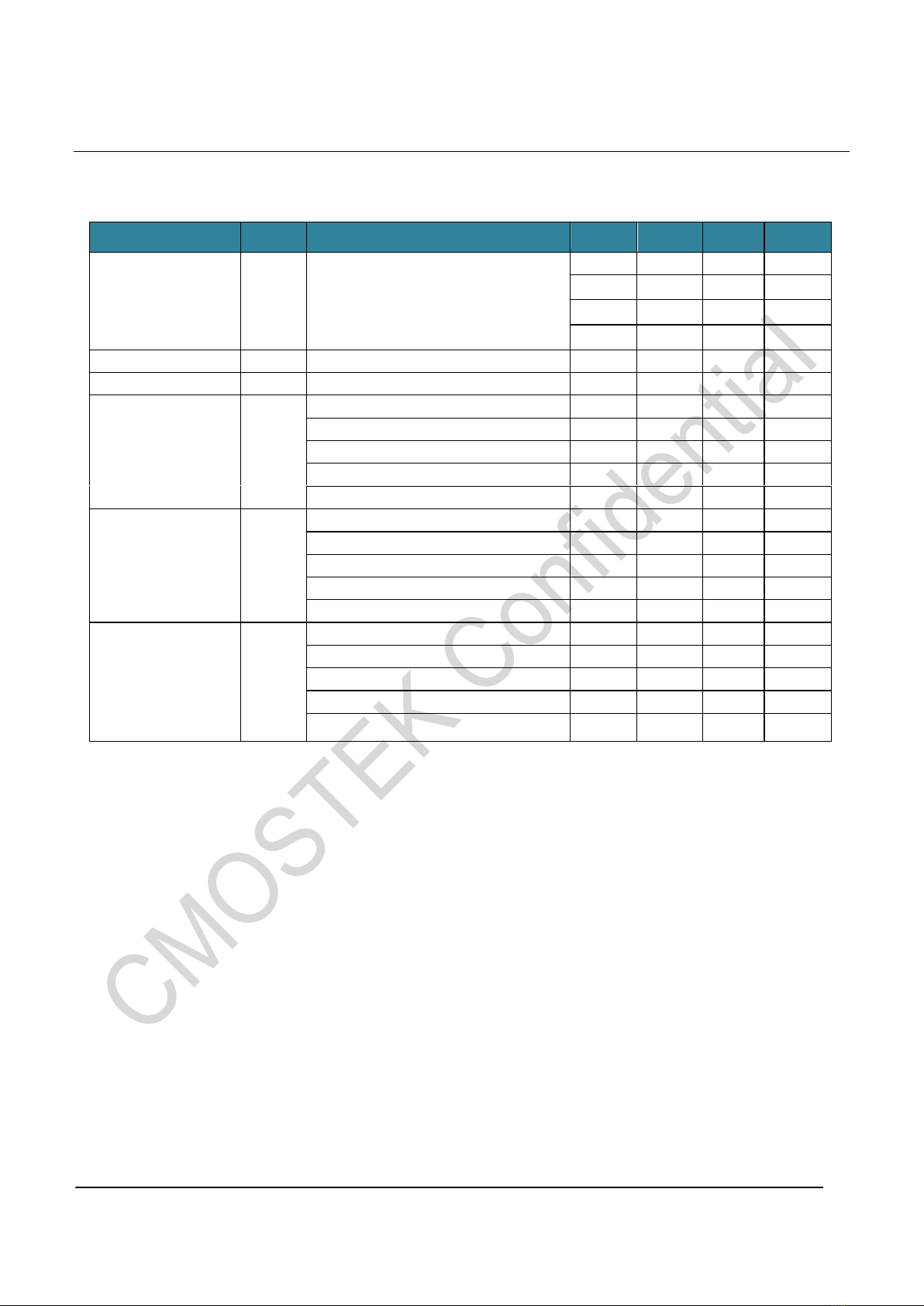
Parameter
Symbol
Condition
Min.
Typ.
Max.
Unit
AlternateChannel
Rejection Ratio
ACR-II
DR = 10 kbps, FDEV = 10 kHz; BW=100kHz, 400
kHz Channel spacing, interference with the same
modulation
45
dBc
Blocking Rejection
Ratio
BI
DR = 10 kbps, FDEV = 10 kHz; ±1 MHz Deviation,
continuous wave interference
70
dBc
DR = 10 kbps, FDEV = 10 kHz; ±2 MHz Deviation,
continuous wave interference
72
dBc
DR = 10 kbps, FDEV = 10 kHz; ±10 MHz Deviation,
continuous wave interference
75
dBc
Input 3rd Order
Intercept Point
IIP3
DR = 10 kbps, FDEV = 10 kHz; 1 MHz and 2 MHz
Deviation dual tone test, maximum system gain
setting.
-25
dBm
RSSIRange
RSSI
-120
20
dBm
More Sensitivity
(Typical Configuration)
433.92 MHz, DR = 1.2kbps, FDEV = 5 kHz
-122.9
dBm
433.92 MHz, DR = 1.2kbps, FDEV = 10 kHz
-121.8
dBm
433.92 MHz, DR = 1.2kbps, FDEV = 20 kHz
-119.5
dBm
433.92 MHz, DR = 2.4kbps, FDEV = 5 kHz
-120.6
dBm
433.92 MHz, DR = 2.4kbps, FDEV = 10 kHz
-120.3
dBm
433.92 MHz, DR = 2.4kbps, FDEV = 20 kHz
-119.7
dBm
433.92 MHz, DR = 9.6 kbps, FDEV = 9.6 kHz
-116.0
dBm
433.92 MHz, DR = 9.6 kbps, FDEV = 19.2 kHz
-116.1
dBm
433.92 MHz, DR = 20 kbps, FDEV = 10 kHz
-114.2
dBm
433.92 MHz, DR = 20 kbps, FDEV = 20 kHz
-113.0
dBm
433.92 MHz, DR = 50 kbps, FDEV = 25 kHz
-110.6
dBm
433.92 MHz, DR = 50 kbps, FDEV = 50 kHz
-109.0
dBm
433.92 MHz, DR = 100 kbps, FDEV = 50 kHz
-107.8
dBm
433.92 MHz, DR = 200 kbps, FDEV = 50 kHz
-103.5
dBm
433.92 MHz, DR = 200 kbps, FDEV = 100 kHz
-104.3
dBm
433.92 MHz, DR = 300 kbps, FDEV = 50 kHz
-98.0
dBm
433.92 MHz, DR = 300 kbps, FDEV = 150 kHz
-101.6
dBm

CMT2300A
Rev1.0a | 8/50
www.cmostek.com
1.5 Transmitter
Table 5. Transmitter Specifications
Parameter
Symbol
Condition
Min.
Typ.
Max.
Unit
Output power
POUT
Need specific peripheral materials for
different frequency bands
-20
+20
dBm
Output power step
PSTEP
1
dB
GFSK Gaussian filter
coefficient
BT
0.3
0.5
1.0
-
Output power variation
POUT-TOP
Temperature from -40 to +85 C
1
dB
Stray radiation
POUT = +13 dBm,433MHz, FRF<1 GHz
-42
dBm
1 GHz to 12.75 GHz, with harmonic
-36
dBm
Harmonic output for
FRF= 433 MHz[1]
H2433
2ndharmonic +20 dBm POUT
-46
dBm
H3433
3ndharmonic +20 dBm POUT
-50
dBm
Harmonic output for
FRF= 868 MHz[1]
H2868
2ndharmonic +20 dBm POUT
-43
dBm
H3868
3ndharmonic +20 dBm POUT
-52
dBm
Harmonic output for
FRF= 915 MHz[1]
H2868
2ndharmonic +20 dBm POUT
-48
dBm
H3868
3ndharmonic +20 dBm POUT
-53
dBm
Harmonic output for
FRF= 433 MHz[1]
H2433
2ndharmonic +13 dBm POUT
-52
dBm
H3433
3ndharmonic +13 dBm POUT
-52
dBm
Harmonic output for
FRF= 868 MHz[1]
H2868
2ndharmonic +13 dBm POUT
-52
dBm
H3868
3ndharmonic +13 dBm POUT
-52
dBm
Harmonic output for
FRF= 915 MHz[1]
H2868
2ndharmonic +13 dBm POUT
-52
dBm
H3868
3ndharmonic +13 dBm POUT
-52
dBm
Notes:
[1]. The harmonic parameter values mainly depend on the quality of the hardware matching network. The above data is
measured based on the CMT2300A-EM module.
1.6 Settling Time
Table 6. Settling Time
Parameter
Symbol
Condition
Min.
Typ.
Max.
Unit
Settle time
TSLP-RX
From Sleep to RX
1000
us
TSLP-TX
From Sleep to TX
1000
us
TSTB-RX
From Standby to RX
350
us
TSTB-TX
From Standby to TX
350
us
TRFS-RX
From RFS to RX
20
us
TTFS-RX
From TFS to TX
20
us
TTX-RX
From TX to RX
(Ramp Down time needs 2Tsymbol )
2Tsymbol
+350
us
TRX-TX
From RX to TX
350
us
Notes:
[1]. TSLP-RX and TSLP-TX depend on the crystal oscillator startup time, which is related to crystal characteristics.
CMT2300A
Rev1.0a | 9/50
www.cmostek.com
1.7 Frequency Synthesizer
Table 7. Frequency Synthesizer Specifications
Parameter
Symbol
Condition
Min.
Typ.
Max.
Unit
Frequency range
FRF
Need different matching networks
760
1020
MHz
380
510
MHz
190
340
MHz
127
170
MHz
Frequency resolution
FRES
25
Hz
Frequency tuning time
tTUNE
150
us
Phase noise@ 433
MHz
PN433
10 kHz frequency deviation
-94
dBc/Hz
100 kHz frequency deviation
-99
dBc/Hz
500 kHz frequency deviation
-118
dBc/Hz
1MHz frequency deviation
-127
dBc/Hz
10 MHz frequency deviation
-134
dBc/Hz
Phase noise@ 868
MHz
PN868
10 kHz frequency deviation
-92
dBc/Hz
100 kHz frequency deviation
95
dBc/Hz
500 kHz frequency deviation
-114
dBc/Hz
1MHz frequency deviation
-121
dBc/Hz
10 MHz frequency deviation
-130
dBc/Hz
Phase noise@ 915
MHz
PN915
10 kHz frequency deviation
-89
dBc/Hz
100 kHz frequency deviation
-92
dBc/Hz
500 kHz frequency deviation
-111
dBc/Hz
1MHz frequency deviation
-121
dBc/Hz
10 MHz frequency deviation
-130
dBc/Hz
CMT2300A
Rev1.0a | 10/50
www.cmostek.com
1.8 Crystal Oscillator
Table 8. Crystal Oscillator Specifications
Parameter
Symbol
Condition
Min.
Typ.
Max.
Unit
Crystal frequency[1]
FXTAL
26
MHz
Frequency tolerance[2]
ppm
20
ppm
Load capacitance
CLOAD
15
pF
Equivalent resistance
Rm
60
Ω
Start-up time[3]
tXTAL
400
us
Notes:
[1]. CMT2300Acan use the external reference clock to drive the XIN pin through the coupling capacitor. The peak value of
the external clock signal is between 0.3V and 0.7V.
[2]. The value includes (1) initial error; (2) crystal load; (3) aging; and (4) change with temperature. The acceptable crystal
frequency tolerance is limited by the receiver bandwidth and the RF frequency offset between the transmitter and the
receiver.
[3]. The parameter is largely related to the crystal.
1.9 Low Frequency Oscillator
Table 9. Low Frequency Oscillator Specifications
Parameter
Symbol
Condition
Min.
Typ.
Max.
Unit
Calibration frequency [1]
FLPOSC
32
kHz
Frequency accuracy
After calibration
±1
%
Temperature coefficient [2]
-0.02
%/°C
Supply voltage coefficient [3]
+0.5
%/V
Initial calibration time
tLPOSC-CAL
4
ms
Notes:
[1]. The low frequency oscillator is automatically calibrated to the crystal oscillator frequency at the PUP stage and
periodically calibrated at this stage.
[2]. After calibration, the frequency changes with temperature.
[3]. After calibration, the frequency changes with the change of the supply voltage.
www.cmostek.com
Rev1.0a | 11/50
CMT2300A
1.10Low Battery Detection
Table 10. Low Battery Detection Specifications
Parameter
Symbol
Condition
Min.
Typ.
Max.
Unit
Detection accuracy
LBDRES
50
mV
1.11Digital Interface
Table 11.Digital interface specifications
Parameter
Symbol
Condition
Min.
Typ.
Max.
Unit
Digital input high level
VIH
0.8
VDD
Digital input low level
VIL
0.2
VDD
Digital output high level
VOH
@IOH= -0.5mA
Vdd-0.4
V
Digital output low level
VOL
@IOL= 0.5mA
0.4
V
SCLK Frequency
FSCL
5
MHz
SCLK high time
TCH
50
ns
SCLK low time
TCL
50
ns
SCLKrise time
TCR
50
ns
SCLKfall time
TCF
50
ns
1.12Figures of Critical Parameters
1.12.1 Rx Current VS. Supply Voltage
Testing Condition: Freq = 434MHz / 868MHz, Fdev = 10KHz, BR = 10Kbps
7.40
7.60
7.80
8.00
8.20
8.40
8.60
8.80
3.6
3.5
3.4
3.3
3.2
3.1
3.0
2.9
2.8
2.7
2.6
2.5
2.4
2.3
2.2
2.1
2.0
1.9
1.8
Current Comsumption(mA)
Supply Voltage(V)
Rx Current vs. Supply Voltage
434MHz
868MHz

www.cmostek.com
Rev1.0a | 12/50
CMT2300A
1.12.2 Rx Current VS. Voltage Temperature
Test Condition: Freq = 434MHz,Fdev = 10KHz, BR = 10Kbps
Test Condition: Freq = 868MHz, Fdev = 10KHz, BR = 10Kbps
1.12.3 Sensitivity VS. Voltage
7.0
7.3
7.5
7.8
8.0
8.3
8.5
8.8
9.0
9.3
9.5
-40
25
85
Current Consumption(mA)
Temperature(℃)
Rx Current vs. Volt-Temp
3.3V
1.8V
3.6V
7.0
7.3
7.5
7.8
8.0
8.3
8.5
8.8
9.0
9.3
9.5
-40
25
85
Current Consumption(mA)
Temperature(℃)
Rx Current vs. Volt-Temp
3.3V
1.8V
3.6V
www.cmostek.com
Rev1.0a | 13/50
CMT2300A
Test Condition: FSK modulation, DEV = 10KHz, BR = 10Kbps
1.12.4 Sensitivity VS. Temperature
Test Condition: FSK, DEV = 10KHz, BR = 10Kbps
-117.5
-117.0
-116.5
-116.0
-115.5
-115.0
-114.5
-114.0
-113.5
-113.0
1.8
2.1
2.4
2.8
3.0
3.3
3.6
Sensitivity(dBm)
Supply Voltage(V)
Sensitivity vs. Voltage
434MHz
868MHz
-118.0
-117.0
-116.0
-115.0
-114.0
-113.0
-112.0
-40
25
85
Sensitivity(dBm)
Temperature(℃)
Sensitivity vs. Temperature
434MHz
868MHz

www.cmostek.com
Rev1.0a | 14/50
CMT2300A
1.12.5 Tx Power VS. Supply Voltage
Test Condition: Freq = 434 MHz, 20 dBm / 13dBm matching network
Test Condition: Freq = 868 MHz, 20 dBm / 13dBm matching network
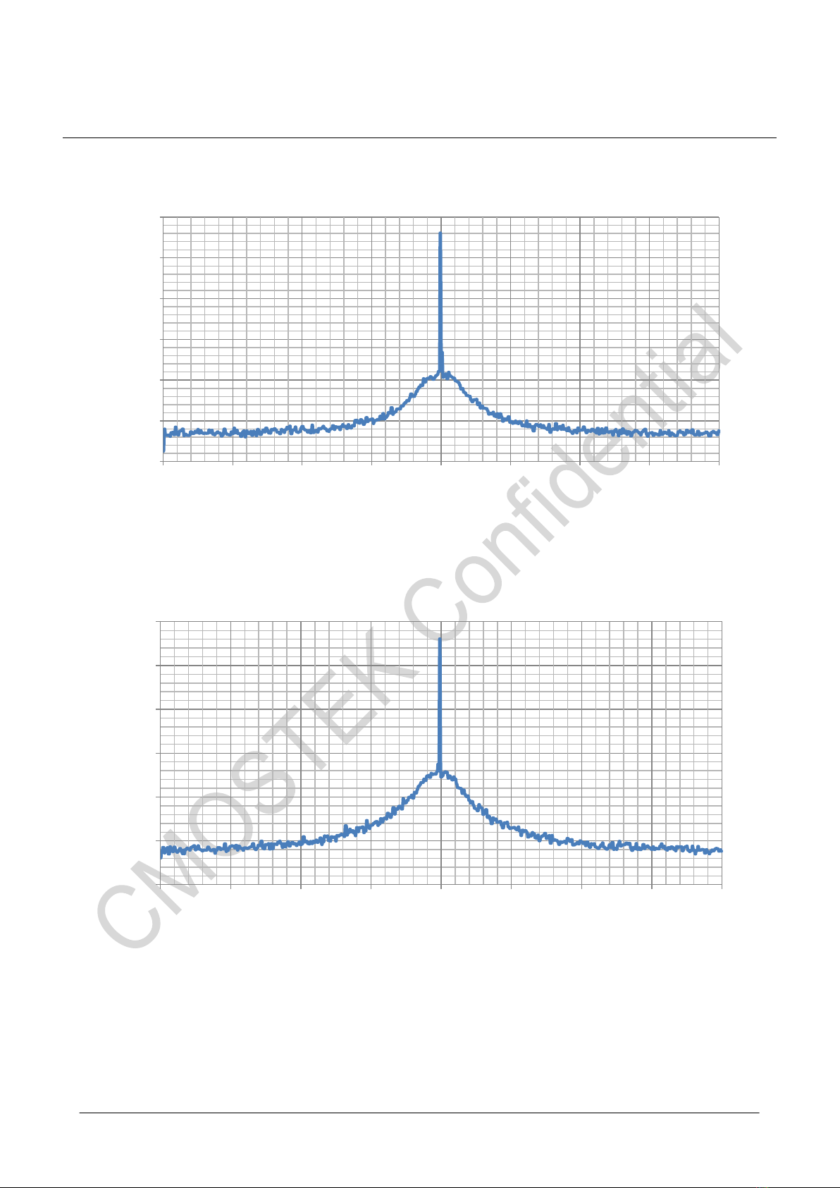
1.12.6 Tx Phase Noise
10.0
11.0
12.0
13.0
14.0
15.0
16.0
17.0
18.0
19.0
20.0
3.6
3.5
3.4
3.3
3.2
3.1
3.0
2.9
2.8
2.7
2.6
2.5
2.4
2.3
2.2
2.2
2.1
2.0
1.9
1.8
Tx Power(dBm)
Supply Voltage(V)
Tx Power vs. Supply Voltage
20dBm
13dBm
9.0
10.0
11.0
12.0
13.0
14.0
15.0
16.0
17.0
18.0
19.0
20.0
3.6
3.5
3.4
3.3
3.2
3.1
3.0
2.9
2.8
2.7
2.6
2.5
2.4
2.3
2.2
2.1
2.1
2.0
1.9
1.8
Tx Power(dBm)
Supply Voltage(V)
Tx Power vs. Supply Voltage
13dBm
20dBm
www.cmostek.com
Rev1.0a | 15/50
CMT2300A
13.4dBm
-100
-80
-60
-40
-20
0
20
431.92 432.42 432.92 433.42 433.92 434.42 434.92 435.42 435.92
Power (dBm)
center 433.92MHz sweep 5s (2000pts )
Res BW 1kHz
433.92MHz Phase Noise
output 13dBm span=4MHz
att30dB
12.4dBm
-100
-80
-60
-40
-20
0
20
866 866.5 867 867.5 868 868.5 869 869.5 870
Power (dBm)
center 868MHz sweep 5s (2000pts )
Res BW 1kHz
868MHz Phase Noise
output 13dBm span=4MHz
att30dB
www.cmostek.com
Rev1.0a | 16/50
CMT2300A
2.Pin Descriptions
17
GND
SCLK
SDIO
CSB
FCSB
XI
XO
GPIO2
GPIO1
AVDD
PA
RFIN
RFIP
GPIO3
DVDD
DGND
AGND
13
14
15
16
1
2
3
4
5678
9
10
11
12
Figure 1. CMT2300Apin descriptions
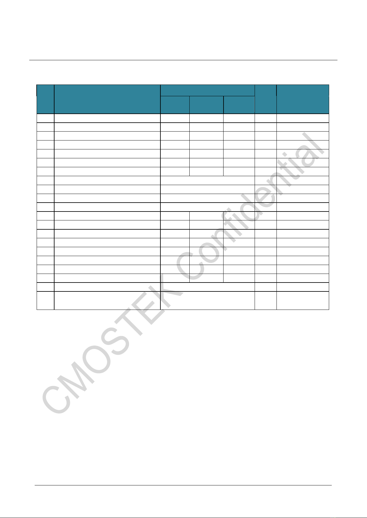
Table 12. CMT2300APin Descriptions
Pin #
Name
I/O
Internal IO Schematic
Descriptions
1
RFIP
I
RF signal input P
2
RFIN
I
RF signal input N
3
PA
O
PA output
4
AVDD
IO
Analog VDD
5
AGND
IO
Analog GND
6
DGND
IO
Digital GND
7
DVDD
IO
Digital VDD
8[1]
GPIO3
IO
GPIO3
din
pd_din
dout
pd_dout
Data tristate
pd_din default value is “1”
pd_dout default value is “0”
VDD
Configured as CLKO,
DOUT/DIN, INT2 and
DCLK (TX/RX)
9
SCLK
I
SCLK din
Buffer
VDD
SPI clock

www.cmostek.com
Rev1.0a | 17/50
CMT2300A
Pin #
Name
I/O
Internal IO Schematic
Descriptions
10
SDIO
IO
SDIO
din
pd_din
dout
pd_dout
Data tristate
pd_din default value is “0”
pd_dout default value is “1”
VDD
SPI data input and output
11
CSB
I
CSB Buffer
VDD
SPI chip selection bar for
register access, active low
12
FCSB
I
FCSB Buffer
VDD
SPI chip selection bar for
FIFO access, active low
13
XI
I
Crystal circuit input
14
XO
O
Crystal circuit output
15[1]
GPIO2
IO
GPIO2
din
pd_din
dout
pd_dout
Data tristate
pd_din default value is “1”
pd_dout default value is “0”
VDD
Configured as INT1, INT2,
DOUT/DIN, DCLK
(TX/RX) and RF_SWT
16[1]
GPIO1
IO
GPIO1
din
pd_din
dout
pd_dout
Data tristate
pd_din default value is “1”
pd_dout default value is “0”
VDD
Configured as DOUT/DIN,
INT1, INT2, DCLK
(TX/RX) and RF_SWT
17
GND
I
Analog GND. It must be
grounded.
Notes:
[1]. [1]INT1 and INT2 are interrupts. DOUT is demodulated output. DIN is a modulation input. DCLK is a modulation or demodulation
data rate synchronization clock, automatic switching in TX/RX mode.

www.cmostek.com
Rev1.0a | 18/50
CMT2300A
3.Typical Application Schematic
3.1 Direct Tie Schematic Diagram
Figure 2. Direct Tie Application Schematic Diagram
Table 13. 13 dBm direct tie application BOM
No.
Descriptions
Values
Unit
Supplier
433 MHz
+13 dBm
868 MHz
+13dBm
915 MHz
+13dBm
C1
±5%, 0603 NP0, 50 V
15
22
22
pF
C2
±5%, 0603 NP0, 50 V
5.6
6.2
6.2
pF
C3
±5%, 0603 NP0, 50 V
7.5
3.6
3.3
pF
C4
±5%, 0603 NP0, 50 V
24
24
24
pF
C5
±5%, 0603 NP0, 50 V
24
24
24
pF
C6
±5%, 0603 NP0, 50 V
4.7
2.2
2.2
pF
C7
±5%, 0603 NP0, 50 V
4.7
2.2
2.2
pF
C8
±5%, 0603 NP0, 50 V
4.7
uF
C9
±5%, 0603 NP0, 50 V
470
pF
C10
±5%, 0603 NP0, 50 V
0.1
uF
C11
±5%, 0603 NP0, 50 V
0.1
uF
L1
±5%, 0603 Multilayer chip inductor
180
100
100
nH
Sunlord SDCL
L2
±5%, 0603 Multilayer chip inductor
56
10
8.2
nH
Sunlord SDCL
L3
±5%, 0603 Multilayer chip inductor
39
8.2
6.8
nH
Sunlord SDCL
L4
±5%, 0603 Multilayer chip inductor
18
10
8.2
nH
Sunlord SDCL
L5
±5%, 0603 Multilayer chip inductor
18
10
8.2
nH
Sunlord SDCL
L6
±5%, 0603 Multilayer chip inductor
27
15
12
nH
Sunlord SDCL
L7
±5%, 0603 Multilayer chip inductor
27
15
12
nH
Sunlord SDCL
L8
±5%, 0603 Multilayer chip inductor
68
12
12
nH
Sunlord SDCL
Y1
±10 ppm, SMD32*25 mm
26
MHz
EPSON
U1
CMT2300A, Ultra Low Power Sub-1GHz RF
Transceiver
-
CMOSTEK
www.cmostek.com
Rev1.0a | 19/50
CMT2300A
Table 14. 20 dBm Direct Tie Application BOM
No.
Descriptions
Values
Unit
Supplier
433 MHz
+20 dBm
868 MHz
+20 dBm
915 MHz
+20 dBm
C1
±5%, 0603 NP0, 50 V
15
18
18
pF
C2
±5%, 0603 NP0, 50 V
3.0
3.6
3.6
pF
C3
±5%, 0603 NP0, 50 V
6.2
3.3
3.3
pF
C4
±5%, 0603 NP0, 50 V
24
24
24
pF
C5
±5%, 0603 NP0, 50 V
24
24
24
pF
C6
±5%, 0603 NP0, 50 V
4.7
2
1.8
pF
C7
±5%, 0603 NP0, 50 V
4.7
2
1.8
pF
C8
±5%, 0603 NP0, 50 V
4.7
uF
C9
±5%, 0603 NP0, 50 V
470
pF
C10
±5%, 0603 NP0, 50 V
0.1
uF
C11
±5%, 0603 NP0, 50 V
0.1
uF
L1
±5%, 0603 Multilayer chip inductor
180
100
100
nH
Sunlord SDCL
L2
±5%, 0603 Multilayer chip inductor,
22
12
12
nH
Sunlord SDCL
L3
±5%, 0603 Multilayer chip inductor
cap 15pF
15
15
nH
Sunlord SDCL
L4
±5%, 0603 Multilayer chip inductor
33
6.2
6.2
nH
Sunlord SDCL
L5
±5%, 0603 Multilayer chip inductor
33
6.2
6.2
nH
Sunlord SDCL
L6
±5%, 0603 Multilayer chip inductor
27
15
15
nH
Sunlord SDCL
L7
±5%, 0603 Multilayer chip inductor
27
15
15
nH
Sunlord SDCL
L8
±5%, 0603 Multilayer chip inductor
68
12
12
nH
Sunlord SDCL
Y1
±10 ppm, SMD32*25 mm
26
MHz
EPSON
U1
CMT2300A, Ultra Low Power Sub-1GHz RF
Transceiver
-
CMOSTEK

Table of contents
Other CMOSTEK Transceiver manuals

CMOSTEK
CMOSTEK CMT2380F17 User manual

CMOSTEK
CMOSTEK CMT2380F64 User manual

CMOSTEK
CMOSTEK CMT2300A User manual

CMOSTEK
CMOSTEK CMT2300AW Instruction Manual

CMOSTEK
CMOSTEK CMT2300A User manual

CMOSTEK
CMOSTEK CMT2300A Operating manual

CMOSTEK
CMOSTEK CMT2310A User manual

CMOSTEK
CMOSTEK CMT216 Series User manual

CMOSTEK
CMOSTEK CMT2300A User manual


