CMOSTEK CMT2300A Operating manual

AN146
Rev 0.9 | Page 1/25
www.cmostek.com
Summary
This paper introduces the configuration and use method of the low power consumption of CMT2300A.
The part numbers covered by this document are as shown below.
Table1. Part Numbers Covered by This Document
Part No.
Frequency
Modem
Function
Configuration
Package
CMT2300A
127 - 1020MHz
(G)FSK/OOK
Transceiver
Register
QFN16
Before reading this document, it is recommended that reading the《AN142 - CMT2300A Quick Start
Guideline》,that will be make it easy to understand.
AN146
CMT2300A Low Power Mode Usage Guide
Copyright © By CMOSTEK

AN146
Rev 0.9 | Page 2/25
www.cmostek.com
Table of Contents
Summary............................................................................................................................................................ 1
1. Duty-Cycle Operation Mode ...................................................................................................................... 4
1.1 Duty-Cycle Mode Related Register ................................................................................................. 4
1.2 RX Duty-Cycle Mode....................................................................................................................... 6
1.2.1 Control Full Manually .......................................................................................................... 6
1.2.2 Automatically Wake from SLEEP ......................................................................................... 7
1.2.3 Automatically Wake from SLEEP, Automatically Enter RX................................................... 7
1.2.4 Automatically Wake from SLEEP, Automatically Exit from RX............................................. 8
1.2.5 Receive Full Automatically .................................................................................................. 9
1.3 TX Duty-Cycle Mode ....................................................................................................................... 9
1.3.1 Automatically Exit from TX................................................................................................ 10
1.3.2 Automatically Wake from SLEEP, Automatically Exit from TX ........................................... 10
1.3.3 Transmit Full Automatically............................................................................................... 11
1.4 Enter and Exit from Duty-Cycle Mode .......................................................................................... 11
1.4.1 Enter Duty-Cycle Mode ..................................................................................................... 11
1.4.2 Exit from Duty-Cycle Mode ............................................................................................... 11
2. Supper Low Power(SLP) Receiving Mode ................................................................................................ 13
2.1 Register associated with SLP receiving ......................................................................................... 13
2.2 Basic Principles of Low Power Transceiver ................................................................................... 13
2.3 Channel Sensing ........................................................................................................................... 14
2.3.1 Register associated with channel sensing......................................................................... 15
2.3.2 RSSI Contrast ..................................................................................................................... 16
2.3.3 Phase Jump Detector (PJD)................................................................................................ 16
2.4 SLP Receiving Mode Detail ........................................................................................................... 17
2.4.1 SLP Pattern 0 ..................................................................................................................... 18
2.4.2 SLP Pattern 1~3 ................................................................................................................. 19
2.4.3 SLP Pattern 4 ..................................................................................................................... 20
2.4.4 SLP Pattern 5-10 ................................................................................................................ 21
2.4.5 SLP Pattern 11-13.............................................................................................................. 22

AN146
Rev 0.9 | Page 3/25
www.cmostek.com
3. Document Modification Record............................................................................................................... 23
4. Contact Information................................................................................................................................. 25

AN146
Rev 0.9 | Page 4/25
www.cmostek.com
1. Duty-Cycle Operation Mode
1.1 Duty-Cycle Mode Related Register
The corresponding RFPDK interface and parameters are as below:
Figure 1. Duty-Cycle RFPDK Interface
Table 2. Duty-Cycle Related Parameter
Register Bit RFPDK Parameter
Register Bit
Rx Duty-Cycle
RX_DC_EN
Tx Duty-Cycle
TX_DC_EN
Sleep Timer
SLEEP_TIMER_EN
Sleep Time
SLEEP_TIMER_M<10:0>
SLEEP_TIMER_R<3:0>
Rx Timer
RX_TIMER_EN
Rx Time T1
RX_TIMER_T1_M<10:0>
RX_TIMER_T1_R<3:0>
Rx Time T2
RX_TIMER_T2_M<10:0>
RX_TIMER_T2_R<3:0>
Rx Exit State
RX_EXIT_STATE<1:0>
Tx Exit State
TX_EXIT_STATE<1:0>
LFOSC Calibration
LFOSC_RECAL_EN
LFOSC_CAL1_EN
LFOSC_CAL2_EN
XTAL Stable Time
XTAL_STB_TIME<2:0>
The contents and explanations of the register can be seen in the following table.
Table3. Register Located in the Configuration Bank:
Register
Name
Bits
R/W
Bit Name
Function Description
CUS_SYS2
(0x0D)
7
RW
LFOSC_RECAL_EN
Enable LFOSC recalibration 1. Before you
enter the RX or TX every time, if you find the
last result of the calibration 2 beyond the
boundary, that is not to tune the frequency by
the fine adjustment, the calibration 1 can
automatically run again, This calibration will

AN146
Rev 0.9 | Page 5/25
www.cmostek.com
Register
Name
Bits
R/W
Bit Name
Function Description
cost about several milliseconds.
0:Disable
1:Enable
6
RW
LFOSC_CAL1_EN
Enable LFOSC Calibration 1, the calcultion
will only be done once after the power is on
or reset. Ensure that the frequency of the
LFOSC is roughly adjusted to 32 kHz. This
calculation will cost 5 milliseconds.
0:Disable
1:Enable
5
RW
LFOSC_CAL2_EN
Enable LFOSC Calibration 2, the calcultion
will be runing continuously in the RX or TX
status ,Ensure that the frequency of the
LFOSC is more accurate adjusted to 32
kHz.. This correction is done in parallel in the
TX or RX status. The enabling condition is
that the LFOSC_CAL1_EN must be enabled.
0:Disable
1:Enable
4
RW
RX_TIMER_EN
Enable RX timer
0:Disable
1:Enable
3
RW
SLEEP_TIMER_EN
Enable SLEEP timer
0:Disable
1:Enable
2
RW
TX_DC_EN
Enable TX Duty Cycle
0:Disable
1:Enable
1
RW
RX_DC_EN
Enable RX Duty Cycle
0:Disable
1:Enable
0
RW
DC_PAUSE
Suspend Duty Cycle
0:NO suspend
1:Suspend
CUS_SYS3
(0x0E)
7
RW
SLEEP_BYPASS_EN
This bit must keep 0.
6:4
RW
XTAL_STB_TIME<2:0>
Crystal stability time:
0:19.5 us
1:39 us
2:78 us
3:155 us
4:310 us
5:620 us
6:1240 us
7:2480 us
3:2
RW
TX_EXIT_STATE<1:0>
Automatically exit to the preset status after
transmitting,it is only valid in the packet
mode. otherwise, the chip will not
automatically exit from the TX status, but
wait for the MCU to send go_* command to
switch.
0:SLEEP
1:STBY
2:TFS

AN146
Rev 0.9 | Page 6/25
www.cmostek.com
Register
Name
Bits
R/W
Bit Name
Function Description
3:NA
1:0
RW
RX_EXIT_STATE<1:0>
Automatically exit to the preset status after
receiving,it is only valid in the packet mode
and enabling RX Timer, otherwise the chip
will not automatically exit from the RX status,
but wait for the MCU to send go_* command
to switch.
0:SLEEP
1:STBY
2:RFS
3:NA
CUS_SYS4
(0x0F)
7:0
RW
SLEEP_TIMER_M<7:0>
Define the timing time for SLEEP TIMER,
formula as follows:
T = M x 2^(R+1) x 31.25 us
CUS_SYS5
(0x10)
6:4
RW
SLEEP_TIMER_M<10:8>
3:0
RW
SLEEP_TIMER_R<3:0>
CUS_SYS6
(0x11)
7:0
RW
RX_TIMER_T1_M<7:0>
Define the timing time for RX T1 TIMER,
formula as follows:
T = M x 2^(R+1) x 20 us
CUS_SYS7
(0x12)
6:4
RW
RX_TIMER_T1_M<10:8>
3:0
RW
RX_TIMER_T1_R<3:0>
CUS_SYS8
(0x13)
7:0
RW
RX_TIMER_T2_M<7:0>
Define the timing time for RX T2 TIMER,
formula as follows:
T = M x 2^(R+1) x 20 us
CUS_SYS9
(0x14)
6:4
RW
RX_TIMER_T2_M<10:8>
3:0
RW
RX_TIMER_T2_R<3:0>
1.2 RX Duty-Cycle Mode
To control the RX Duty-Cycle mode, 4 register control bits are used. According to the actual application
requirements, here are 5 combinations of the 4 control bits and the corresponding operation mode.
In the following status diagram, the gray line indicates that the MCU manually sends the go_* command
to switch the status, the blue line indicates the chip automatic status switching. Note that switching from the
status A to the status B, once the blue line exists, the gray line cannot exist, and the reverse is also the case.
That is, if the automatic control is adopted, the MCU is not allowed to use the manual control, otherwise it will
disturb the chip operation, there may be a crash situation. If you use the manual switching, the automatic
switching cannot be enabled.
1.2.1 Control Full Manually
Controlling full manually means not opening any Duty-Cycle control.
Table 4. Control Full Manually
Control Bit
Value
SLEEP_TIMER_EN
0
RX_DC_EN
0
RX_TIMER_EN
0
RX_EXIT_STATE
0

AN146
Rev 0.9 | Page 7/25
www.cmostek.com
SLEEP STBY RFS RX
Figure 2. Receiver Controls Full Manually
1.2.2 Automatically Wake from SLEEP
This mode only opens SLEEP TIMER. After automatically awakening, the chip will switch to the STBY
and wait for the MCU operation. Based on the operating principle introduced above, once the chip has
entered the SLEEP, the MCU cannot order the chip to jump out of the SLEEP. It can only wait for the sleep
counter timeout and begin operation until the SL_TMO interrupt is detected.
Table5 Automatically Wake from SLEEP
Control Bit
Value
SLEEP_TIMER_EN
1
RX_DC_EN
0
RX_TIMER_EN
0
RX_EXIT_STATE
0
SLEEP_TIMER_EN = 1
SLEEP STBY RFS RX
Figure3. Receiver Automatically Wakes from Sleep
1.2.3 Automatically Wake from SLEEP, Automatically Enter RX
Open the RX_DC_EN, when the chip automatically wakes from SLEEP, it will not jump to STBY, but will
directly do the PLL correction and switch to the RX to receive. In this mode, the RFS status is not allowed, and
the MCU participation has been greatly reduced.

AN146
Rev 0.9 | Page 8/25
www.cmostek.com
Table 6. Automatically Wake from SLEEP, Automatically Enter RX
Control Bit
Value
SLEEP_TIMER_EN
1
RX_DC_EN
1
RX_TIMER_EN
0
RX_EXIT_STATE
0
SLEEP_TIMER_EN = 1, RX_DC_EN = 1
SLEEP STBY RFS RX
Figure 4. Receiver Automatically Wakes from SLEEP and Automatically Enters RX
1.2.4 Automatically Wake from SLEEP, Automatically Exit from RX
In this mode, based on the automatically waking from SLEEP, add the automatically exiting from RX.
Entering RFS or RX from STBY need the MCU to switch manually (That is not automatically enter the
receiving). But once RX is entered, the RX TIMER will start counting, and when the timeout exits, it will
automatically switch to the corresponding status according to the RX_EXIT_STATE configuration. In general,
the STBY state can be used as a "relay station", the MCU can participate in operations such as clearing the
interrupt and reading the FIFO.
Table 7. Automatically Wake from SLEEP, Automatically Exit from RX
Control Bit
Value
SLEEP_TIMER_EN
1
RX_DC_EN
0
RX_TIMER_EN
1
RX_EXIT_STATE
0/1/2
SLEEP STBY RFS RX
RX_TIMER_EN = 1, RX_EXIT_STATE = 0
RX_TIMER_EN = 1, RX_EXIT_STATE = 1
RX_TIMER_EN = 1,
RX_EXIT_STATE = 2
SLEEP_TIMER_EN = 1
Figure 5. Receiver Automatically Wakes from SLEEP, Automatically Exits from RX

AN146
Rev 0.9 | Page 9/25
www.cmostek.com
1.2.5 Receive Full Automatically
Fully automatic receiving mode, that is, once the operation is started, there is no need the MCU (and not)
to participate in the switching status. The MCU can only obtain the chip working status by the preset interrupt,
and perform the required operation. It should be noted that before entering the full automatic receiving, the
MCU must configure the package format, the FIFO working mode, the interrupt and IO in the STBY status.
Table 8. Receive Full Automatically
Control Bit
Value
SLEEP_TIMER_EN
1
RX_DC_EN
1
RX_TIMER_EN
1
RX_EXIT_STATE
0
SLEEP_TIMER_EN = 1, RX_DC_EN = 1
SLEEP STBY RFS RX
RX_TIMER_EN = 1, RX_EXIT_STATE = 0
Figure 6. Receiver Controls Full Automatically
The mode limitation is that MCU is fast enough, must use the interrupt to interact with the chip and finish
the FIFO reading at RX.
The first thing to note about MCU and CMT2300A cooperation is to obey the operation rule. Once the
automatic controlling is enabled, you can't manually order to do the same status switching. Also, it is important
to note that if the automatic exiting from RX is enabled and the exit status is SLEEP, then the interrupt status
in the control bank2 will be lost after exiting to SLEEP. So if you use the mode, you must think it over. Let MCU
interact securely with the chip, there will not be the situation without the interrupt. Usually we would
recommend users to set RX_EXIT_STATE to 1, which is staying in STBY after automatic exiting from RX,
then all the interrupt status will be retained, the power consumption will be reduced greatly. And after you can
let the MCU safely deal with all the work, and then manually switch to SLEEP.
1.3 TX Duty-Cycle Mode
To control the TX Duty-Cycle mode, 3 register control bits are used. For TX, no TX TIMER, because the
transmitting is active behavior, the power is very large. After transmitting in the packet mode, the default
operation of the chip is to automatically exit from the TX status. Therefore, no special counter is required to
count. The transmitting time depends entirely on the content to be transmitted.
According to the actual application requirements, here are 3 combinations of the 3 control bits and the
corresponding operation mode. The control principle is the same as the RX Duty-Cycle mode.

AN146
Rev 0.9 | Page 10/25
www.cmostek.com
1.3.1 Automatically Exit from TX
The simplest mode is that after TX, according to the different TX_EXIT_STATE, automatically switches to
the corresponding status, and the rest of the situation is switched by MCU manual controlling.
Table 9. Automatically Exit from TX
Control Bit
Value
SLEEP_TIMER_EN
0
TX_DC_EN
0
TX_EXIT_STATE
0/1/2
Figure 7. Transmitter Automatically Exits from TX
1.3.2 Automatically Wake from SLEEP, Automatically Exit from TX
In this mode, besides the automatically exiting from TX, also open the SLEEP TIMER. After automatically
waking, the chip will switch to STBY and wait for the MCU operation.
Table 10. Automatically Wake from SLEEP, Automatically Exit from TX
Control Bit
Value
SLEEP_TIMER_EN
1
TX_DC_EN
0
TX_EXIT_STATE
0/1/2
SLEEP_TIMER_EN = 1
SLEEP STBY TFS TX
TX_EXIT_STATE = 0
TX_EXIT_STATE = 1
TX_EXIT_STATE = 2
Figure8. Transmitter Automatically Wakes from SLEEP, Automatically Exits from TX

AN146
Rev 0.9 | Page 11/25
www.cmostek.com
1.3.3 Transmit Full Automatically
Fully automatic transmitting mode, that is, once the operation is started, there is no need the MCU (and
not) to participate in the switching state. The MCU can only obtain the chip working state by the preset
interrupt, and perform the required operation. It should be noted that before entering the full automatic
transmitting, the MCU must first fill in the data to be transmitted in the STBY state, and configure the package
format, the FIFO working mode, the interrupt and IO.
Table 11. Transmit Full Automatically
Control Bit
Value
SLEEP_TIMER_EN
1
TX_DC_EN
1
TX_EXIT_STATE
0
SLEEP_TIMER_EN = 1, TX_DC_EN = 1
SLEEP STBY TFS TX
TX_TIMER_EN = 1, TX_EXIT_STATE = 0
Figure 9. Transmitter Transmits Full Automatically
1.4 Enter and Exit from Duty-Cycle Mode
1.4.1 Enter Duty-Cycle Mode
After the chip initialization is completed, you can configure the related register to enter the desired
Duty-Cycle mode in the configuration stage. After completing the configuration in the STBY and then manually
entering the SLEEP, the chip will officially begin to operate in accordance with the configuration.
1.4.2 Exit from Duty-Cycle Mode
For non full-automatic Duty-Cycle mode, the system always stops in a certain status and waits for the
MCU operation. The MCU can switch the system back to STBY, and then reconfigure several related registers
according to the configuration process introduced earlier, and then you can exit from the Duty-Cycle mode.
For full-automatic Duty-Cycle mode, whether it is TX or RX, the MCU does not accurately know the chip
operating status, so there must be a 100% reliable mechanism to make the chip to stop running and switch
back to the manual control mode.
Assuming CMT2300A starts the full-automatic Duty-Cycle operation after the initialization configuration
introduced above, the MCU can exit safely by operating the following register bits:

AN146
Rev 0.9 | Page 12/25
www.cmostek.com
1. Set DC_PAUSE to 1, and there are several possibilities:
a) If it is currently in the RX state, it will immediately exit to the STBY state.
b) If it is currently in the TX state, it will exit to the STBY state after sending the set N packets(the
spectrum will be spurious if it exits immetiately).
c) If it is currently in the SLEEP state, it will exit to the STBY state after the sleep timer ends.
d) If it is currently in the TUNE state, it will go to the RX or TX state first, and then switch as the
described above.
2. No matter what kind of possibility, MCU can scan the CHIP_MODE_STA<3:0> register until the chip is
confirmed to have entered the STBY.
3. Reconfiguring the Duty-Cycle associated register will turn off the full-automatic mode(other registers can
also be configured). After completing the configuration, set DC_PAUSE to 0, or else it cannot enter
SLEEP.
4. Send the go_sleep command to let the configuration take effect, the system will stay at SLEEP and wait
for the MCU to continue.
Why does the chip wait until the TX operation is completed or the SLEEP timer is over to switch to STBY
after setting DC_PAUSE to 1? This is to allow the chip 100% guarantee to safely exit from the auto run mode.
Otherwise, the system may receive the command at any time and will exit at any time. This will not guarantee
the reliability. If the user sets a long sleep and does not want to wait that long before exiting, it is
recommended that the user exits in second way. The process is as follows:
1. Set CONF_RETAIN to 1, and if initialization is set, there is no need to do so again. Make sure
SLEEP_BYPASS_EN is set to 0.
2. Send the soft reset or the external reset.
3. Scan the CHIP_MODE_STA<3:0> register until the chip is confirmed to enter the SLEEP state.
4. Send the go_stby command immediately to switch the chip to the STBY mode.
5. Then configure, send go_sleep after completion.
This operation will not use the DC_PAUSE register because the MCU can be sure that the chip can send
the go_stby command after it is initialized to enter the SLEEP status. That is, when the MCU is unable to
confirm exactly what status the chip is in, it cannot send any go_* command to do the manual switching,
otherwise it does not guarantee the reliability and has the chance to crash.
So in general, it's OK to let users use the first method to exit. The second one is used when there is a
special requirement. It is important to note that the two mechanisms that exit from the full-automatic
Duty-Cycle mode must be operated only after the CMT2300A has entered the full-automatic Duty-Cycle mode,
otherwise an operation error occurs.

AN146
Rev 0.9 | Page 13/25
www.cmostek.com
2. Supper Low Power(SLP) Receiving Mode
CMT2300A provides a series of options to help users to achieve the supper low power (SLP) reception
under the different application requirements. These options must be valid when RX_TIMER_EN is set to 1,
that is, when the RX timer is valid. The core content of SLP receiver is how to let the receiver minimize the RX
time without the signal, and appropriately extend the RX time to receive with the signal. Finally, the power
consumption is minimized and the reception effect is stabilized.
2.1 Register associated with SLP receiving
The corresponding RFPDK interface and parameters are as below:
Figure 10. SLP RFPDK Interface
Table 12. SLP Related Parameter
Register Bit RFPDK Parameter
Register Bit
The bit is fixed to 1
RX_AUTO_EXIT_DIS
SLP Mode
RX_EXTEND_MODE<3:0>
The contents and explanations of the register can be seen in the following table.
Table13. Register Located in the Configuration Bank:
Register
Name
Bits
R/W
Bit Name
Function Description
CUS_SYS10
(0x15)
5
RW
RX_AUTO_EXIT_DIS
The bit is fixed to 1
3:0
RW
RX_EXTEND_MODE<3:0>
Define the 14 supper low power (SLP)
receiving patterns. See the following
sections for understanding.
2.2 Basic Principles of Low Power Transceiver
The traditional short distance wireless transceiver system usually achieves the low power transceiver in
the following basic method. CMT2300A is also compatible with this method, and on this basis, expands 13
more power saving solutions. Let's first introduce the most basic solution that can be implemented when
RX_EXTEND_MODE<3:0> is set to 0.

AN146
Rev 0.9 | Page 14/25
www.cmostek.com
One Packet
IDLE
IDLE
IDLE
Length of Packet x 2 +
Packet Gap < RX Time TX Burst Time > RX Cycle
TX starts transmittion
发射数据:
Missed Received
接收时间:
XTAL,
TUNE
RX Sleep
RX Cycle < TX Burst Time
SLEEP
Receiving Sleeping XTAL stabilizing
and Frequency Tuning
t
t
IDLE
SLEEP SLEEP SLEEP
TX starts transmittion
Received
Figure 11. Basic Low Power Transceiver Solution
From the diagram, you can see that only meeting the two computational relationships, RX must be able
to capture the TX data in the Duty-Cycle receiving mode:
1. Entire RX cycle< TX total time of sending N packets per batch
2. RX time> The time that 2 packets plus 1 packet gap
Among of them, a full cycle of RX = RX time+ Sleep time+ Crystal Started and settling time+ PLL
frequency correction time
It can be seen that the basic low power solution is constrained by the computational relation. The user
first needs to make a compromise between the time of SLEEP and the length of transmitting the data, that is,
RX saves power or TX saves power. Second, the user must set the RX time window large enough to 100%
capture the data.
2.3 Channel Sensing
First introduce an important auxiliary mechanism of SLP - channel listening before introducing the various
SLP patterns. This mechanism generates a signal RSSI_VLD by monitoring whether an active signal appears
(1 indicates the presence of the signal and 0 indicates noise). This signal is not only output to the GPIO as an
interrupt, but also to assist the implementation of the SLP as a trigger condition.
There are two mechanisms for channel sensing, namely, PJD (Phase Jump Detector) and RSSI contrast.

AN146
Rev 0.9 | Page 15/25
www.cmostek.com
Figure 12. Channel Sensing Mechanism
It should be noted that the PJD can only be used in FSK mode; the RSSI contrast can be used in both
FSK and OOK modes.
2.3.1 Register associated with channel sensing
The corresponding RFPDK interface and parameters are as below:
Figure 13. Channel Sensing RFPDK Interface
Table 14. Channel Sensing Related Parameter
Register Bit RFPDK Parameter
Register Bit
RSSI Valid Source
CCA_INT_SEL<1:0>
PJD Window
PJD_WIN_SEL<1:0>
The contents and explanations of the register can be seen in the following table.
Table 15. Register Located in the Configuration Bank
Register
Name
Bits
R/W
Bit Name
Function Description
CUS_SYS11
(0x16)
7
RW
PJD_TH_SEL
PJD's hidden configuration bit can be fixed to 0.
6:5
RW
CCA_INT_SEL<1:0>
Channel sensing mode option:
0:Determine whether there is a signal by PJD's
RSSI 对比
相位跳变检测
(PJD)
0
2
1
CCA_INT_SEL<1:0>
RSSI_VLD
RSSI
Contrast
Phase Jump
Detector(PJD)

AN146
Rev 0.9 | Page 16/25
www.cmostek.com
output
1:Determine whether there is a signal by
comparing RSSI.
2:Option 0 and option 1 are both met at the
same time..
3:NA。
Only select option 1 in OOK mode.
CUS_SYS12
(0x17)
7:6
RW
PJD_WIN_SEL<1:0>
This parameter defines how many hops the
PJD needs to detect before deciding whether
the incoming signal is noise or signal.
0:4 inverts
1:6 inverts
2:8 inverts
3: 10 inverts
2.3.2 RSSI Contrast
This function will be described in detail in the next chapter "RSSI measure and contrast". Here's a brief
introduction. The principle of doing RSSI contrast is that the RSSI of the signal or noise is higher than the
threshold, and the RSSI_VLD will be valid, otherwise it will not be valid. The advantage of this method is both
available for FSK and OOK mode. The disadvantage is that the threshold setting needs to be debugged
according to the actual application environment, and avoid being triggered by the noise and interference
signal as much as possible. It is not particularly advantageous to generate RSSI_VLD to assist SLP in this
way, so we are primarily concerned with the following PJD method.
2.3.3 Phase Jump Detector (PJD)
PJD is a new technology. When the chip is FSK demodulated, it is possible to determine whether the
incoming signal is the noise or the useful signal by observing the jump characteristics of the received signal.
PJD thinks that switching the input signal from 0 to 1 or from 1 to 0 is a phase jump. The user just needs to
configure the PJD_WIN_SEL<1:0> to tell the PJD how many times the signal jump needs to be detected
before outputting the result.
2
SYM
2
SYM
1
SYM
1
SYM
1
SYM
1
SYM
Figure 14. Received Signal Jump Diagram
As shown above, a total of 8 symbols are received, but the jump occurs only 6 times, so jump variables
are not equal to the number of symbol. The jump variable is equal to the symbol number only when the
preamble is received. Pay attention to this when the user sets up.
The following chapter will discuss how the RSSI_VLD signal assists to implement the supper low power
(SLP) receiving mode. In general, the more times the PJD inverts, the more reliable the judgment is; the less it

AN146
Rev 0.9 | Page 17/25
www.cmostek.com
is, the faster it will be done. If the received time window is very small, then the number of times will be reduced
to meet the window settings.
According to the test data obtained, in general, if the jumping number is 4 times, it can obtain the very
reliable detection result. That is, the noise is not a useful signal. The useful signal will be detected when
coming.
2.4 SLP Receiving Mode Detail
As mentioned above, the kernel of SLP is to control the RX time to achieve a goal. When there is usually
no useful signal, the RX time is very short and it is only used to detect the arrival of the useful signal. When
the useful signal arrives, the RX time will be extended and it can successfully receive the required packet.
So, SLP is based on the various manual, semi automatic, fully automatic RX Duty-Cycle control modes
introduced earlier, and further controls the RX status. That is, the 14 SLP patterns defined by
RX_EXTEND_MODE<3:0> are all designed to control the RX time. Except the control of the RX state,
whether it is automatic or manual, there is no necessary connection with the SLP itself, and the user can
implement different SLP modes in different RX Duty-Cycle modes.
These 14 SLP patterns are explained in detail below. First of all, we assume that CMT2300A is working in
the RX Duty-Cycle mode, automatically waking from SLEEP, automatically exiting from RX and switching to
STBY, MCU is responsible for switching from STBY to SLEEP, and switching from STBY to RX. All 13 SLP
patterns will evolve on this basis.
Table16. SLP Detailed Examples of the RX Duty-Cycle Mode
Control Bit
Value
SLEEP_TIMER_EN
1
RX_DC_EN
0
RX_TIMER_EN
1
RX_EXIT_STATE
1
SLEEP STBY RFS RX
RX_TIMER_EN = 1, RX_EXIT_STATE = 1
SLEEP_TIMER_EN = 1
Figure15. SLP Detailed Examples of the RX Duty-Cycle Mode
We'll introduce the various SLP patterns based on this RX Duty-Cycle mode. The following is a summary
of the 14 patterns. The T1 and T2 mentioned in the table refer to the RX, T1, and T2 time windows that are
available in the registers.

AN146
Rev 0.9 | Page 18/25
www.cmostek.com
Table 17. SLP 14 Patterns
No.
RX Extension Way
RX Extension Condition
0
If configured as 0, no extension is made.
Leave the RX as soon as the T1 timer is
over.
None
1
Leave T1 once the detection conditions are
met within T1. And give the control to MCU.
RSSI_VLD is valid
2
PREAM_OK is vallid
3
RSSI_VLD and PREAM_OK are both valid.
4
As long as RSSI is detected within T1, exit
from T1 and remain in RX until RSSI is not
satisfied, and then exit RX
RSSI_VLD is valid.
5
Switch to T2 once the detection conditions
are met within T1. Exit from RX after the T2
timer is over.
RSSI_VLD is valid.
6
PREAM_OK is valid.
7
RSSI_VLD and PREAM_OK are both valid.
8
PREAM_OK or SYNC_OK, any one is valid.
9
PREAM_OK or NODE_OK, any one is valid.
10
PREAM_OK, SYNC_OK or NODE_OK, any one
is valid.
11
Switch to T2 once the detection conditions
are met within T1. Exit from T2 once SYNC
is detected within T2. And give the control to
MCU. Otherwise, exit from RX after the T2
timer is over.
RSSI_VLD is valid
12
PREAM_OK is valid
13
RSSI_VLD and PREAM_OK are both valid.
Among the 14 patterns described above, there are several uses of RSSI_VLD as trigger conditions.
Using the RSSI_VLD generated by the PJD to assist the supper low power reception is an innovation of
CMT2300A. The effect is very significant. Users are strongly recommended for use. Option 3 combines the
RSSI_VLD generated by PJD and PREAM_OK to make the judgment term. It adds the reliability and doesn't
add much time.
If option 3 is used, assuming that the transmitter sends a long enough preamble, T1 can be set using the
following method:
Set aside 8 symbols for the receiver to do AFC, the PJD invert number is set to 6, the length of preamble
is set to 4 or 8 symbols, and then add the time of 6-8 symbols for detecting whether RSSI_VLD& PREAM_OK
extension conditions are established. So T1's total time is 14 - 16 symbols. If the crystal frequency of the
transmitting and receiving sides has little deviation, for example, it is far less than the set deviation, and then
the AFC time of the previous 8 symbols may be relatively reduced. These need the user to confirm by the
actual test.
2.4.1 SLP Pattern 0
When the pattern is set to 0, the receiving time is equal to RX T1, without any extension. From the

AN146
Rev 0.9 | Page 19/25
www.cmostek.com
diagram below, the MCU is only responsible for sending go_rx and go_sleep command switching the status.
CMT2300A will perform to automatically wake from sleep and automatically exit from RX, and generate the
corresponding interrupt.
The time of RX and SLEEP, etc. given in the figure is only for illustration, without any special meaning.
RX T1
(30 ms)
SLEEP STBY STBY SLEEP (500 ms) RX T1
(50 ms)
STBY STBYCAL CAL SLEEP
go_rx
RX_TMO
go_sleep go_rx go_sleep
CMT2300A
行为
MCU
控制
SL_TMO SL_TMO RX_TMO
Figure16. SLP Pattern 0
2.4.2 SLP Pattern 1~3
When the pattern is set to 1-3, once the detection condition is met within RX T1, the RX T1 will stop to
count; the chip will stay at RX and give the control to the MCU; otherwise, exit from RX after the RX T1 timer
is over. Three different conditions are as follows:
1:The detection condition is RSSI_VLD valid.
2:The detection condition is PREAM_OK valid.
3:The detection condition is RSSI_VLD and PREAM_OK valid at the same time.
Next, take option 2 as an example to give the timing diagram of TX, MCU, and RX coordination:
RX T1
(10 ms)
SLEEP STBY CAL SLEEP
go_rx
PREAM_OK有效
go_sleep
MCU
操作
Preamble Sync Word Data CRC
RX (等待MCU操作)
PKT_OK有效
TX
数据包
SL_TMO
CMT2300A
行为
Figure17. SLP Pattern 1~3
It should be noted that the preset time for RX T1 is 10ms. However, once the detection condition is met, it
will stop. For example, it stops at 7.5ms. Then it will reset and re timing when it enters the RX next time.

AN146
Rev 0.9 | Page 20/25
www.cmostek.com
The following scenes are more suitable for using patterns 1 to pattern 3:
In some applications, the content transmitted by TX varies greatly, that is, the content of each sending,
the packet length and the number of packages are all uncertain. In this case, when the detection condition is
satisfied and the RX T1 is stopped, the switching rights of the RX is returned to the MCU, and it is better for
MCU to decide how long it will take to receive.
The following is the comparison of the 3 conditions:
The detection condition for option 1 is that RSSI_VLD is the output result of channel sensing. As
described earlier, channel sensing with the aid of PJD, can make a very fast and reliable decision about
whether a useful signal is present. More importantly, it does not need to be limited by the data format; it does
not need TX to send the long Preamble, and so on. Therefore, the advantage of option 1 is that when the RX
T1 window is set to a small size (for example, 5-8 symbols), it can still detect and judge very reliably.
The detection condition for option 2 is that PREAM_OK is the interrupt generated by Packet. This is a
traditional detection condition. Generally, at least 2 bytes or more Preamble lengths are required to ensure
that the detection is reliable. So the advantage is easy to understand, the disadvantage is there is the
Preamble inside the packet format, and the Preamble length transmitted by TX must be long enough
(covering 2 RX T1 and 1 SLEEP time). RX T1 also needs to cover 2 bytes or even longer Preamble to achieve
the reliable detection.
The detection conditions for option 3 are both valid at the same time. This means that the detection
conditions are relatively harsh, very difficult to be triggered by mistake. It is with very high reliability. The
minimum value of RX_PREAM_SIZE for CMT2300A can be set to 4 symbols. If combined with the RSSI_VLD
signal, it will not increase the time of RX T1, but also can achieve the more reliable detection result.
2.4.3 SLP Pattern 4
When the pattern is set to 4, RX T1 will stop the timer as long as RSSI_VLD is detected to be valid within
RX T1, and is always in RX until RSSI_VLD is invalid, and then automatically exits from RX. If RSSI_VLD is
detected to be invalid within RX T1, it will exit from RX after the timer is over.
RX T1
(10 ms)
SLEEP STBY CAL SLEEP
go_rx
RSSI_VLD有效
go_sleep
MCU
操作
噪声 连续发射数据,功率不消失(RSSI一直有效)
RX
RX_TMO
TX
数据包
SL_TMO
CMT2300A
行为
噪声
STBY
Figure18. SLP Pattern 4
Other manuals for CMT2300A
3
Table of contents
Other CMOSTEK Transceiver manuals
CMOSTEK
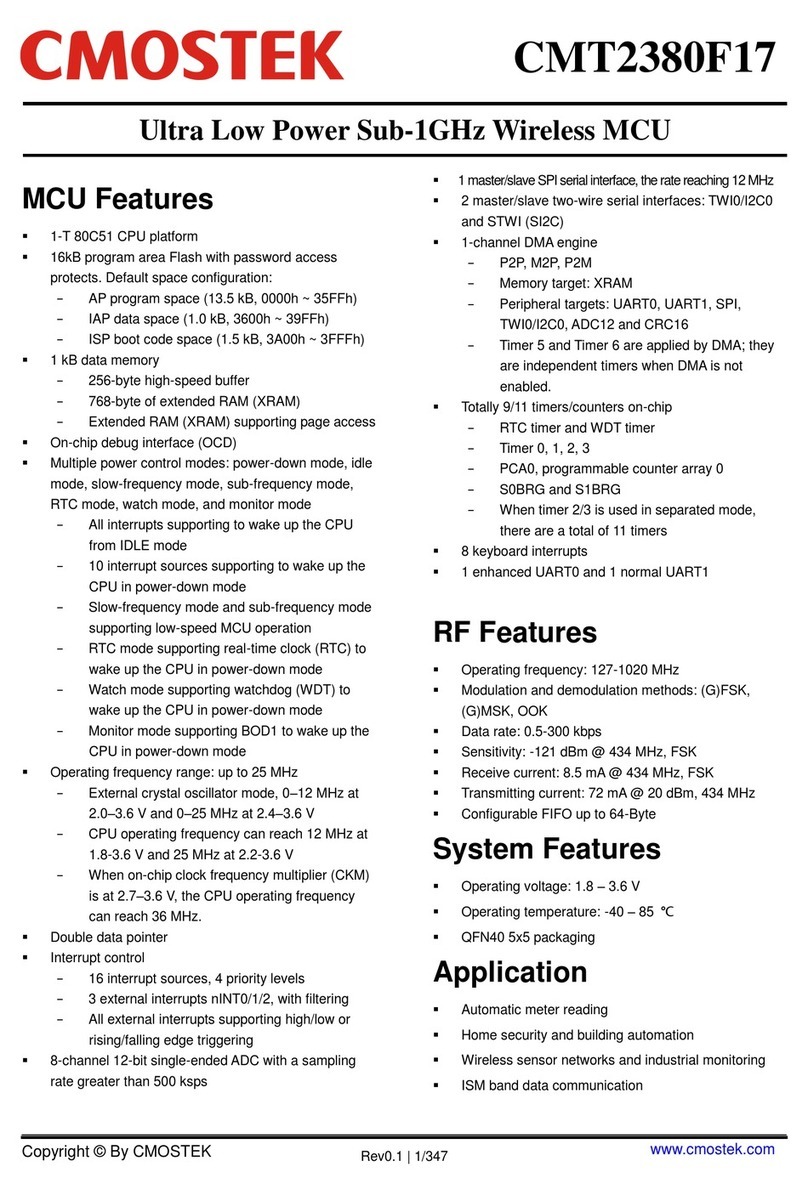
CMOSTEK CMT2380F17 User manual
CMOSTEK
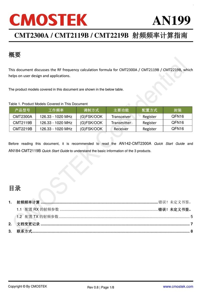
CMOSTEK CMT2300A User manual
CMOSTEK
CMOSTEK CMT2300A User manual

CMOSTEK
CMOSTEK CMT2300A-EQR User manual
CMOSTEK
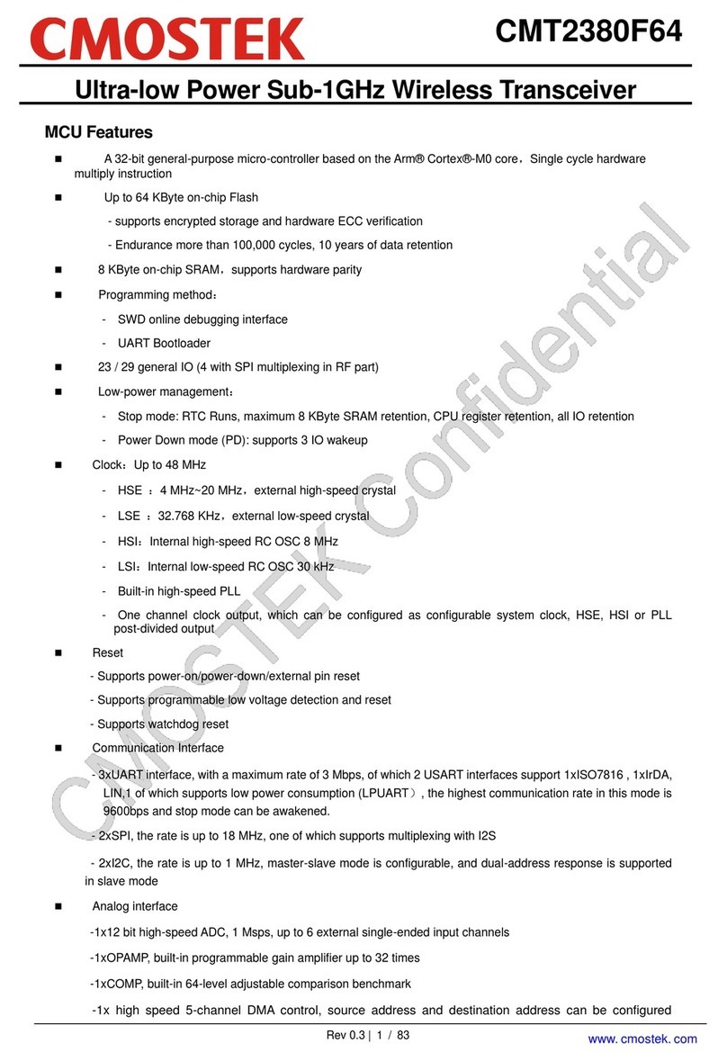
CMOSTEK CMT2380F64 User manual
CMOSTEK
CMOSTEK CMT216 Series User manual

CMOSTEK
CMOSTEK CMT2300AW Instruction Manual
CMOSTEK
CMOSTEK CMT2310A User manual
CMOSTEK
CMOSTEK CMT2300A User manual
Popular Transceiver manuals by other brands
Kenwood
Kenwood NEXEDGE NX-720 instruction manual
Realistic
Realistic TRC-424 owner's manual
Delta Electronics
Delta Electronics Optical Transceiver Modules OPT-155Axxxx Specification sheet
Sommerkamp
Sommerkamp TS-732P instruction manual
Expert Electronics
Expert Electronics SunSDR2 DX user manual
Kenwood
Kenwood TK-3260EX Service manual
