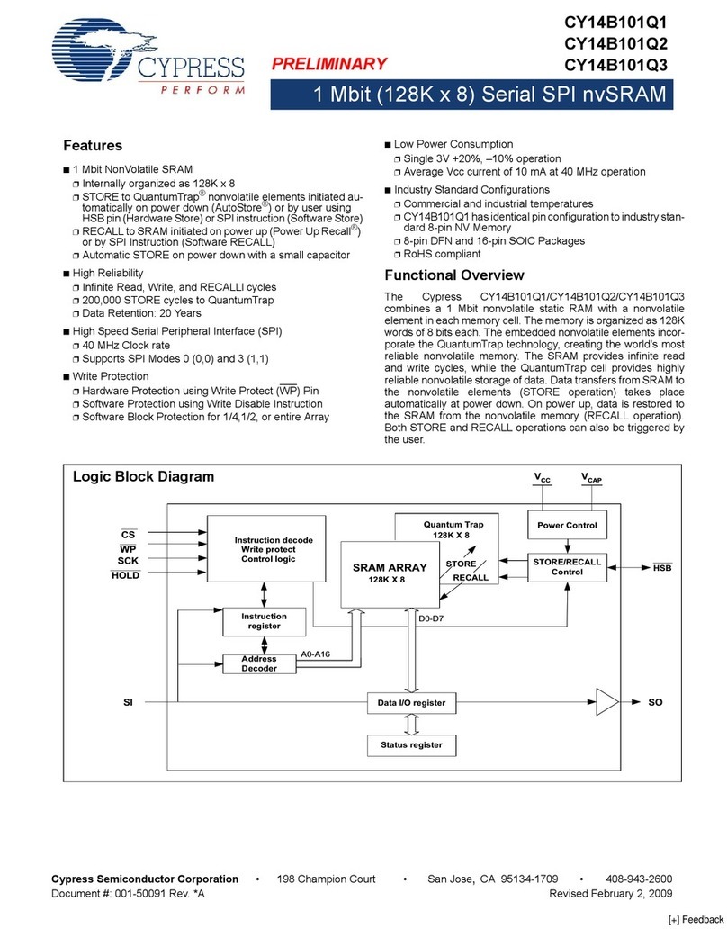
Cypress CY62128B User manual
Other Cypress Computer Hardware manuals
Cypress
Cypress CP-259H User manual

Cypress
Cypress DCT-7 User manual
Cypress
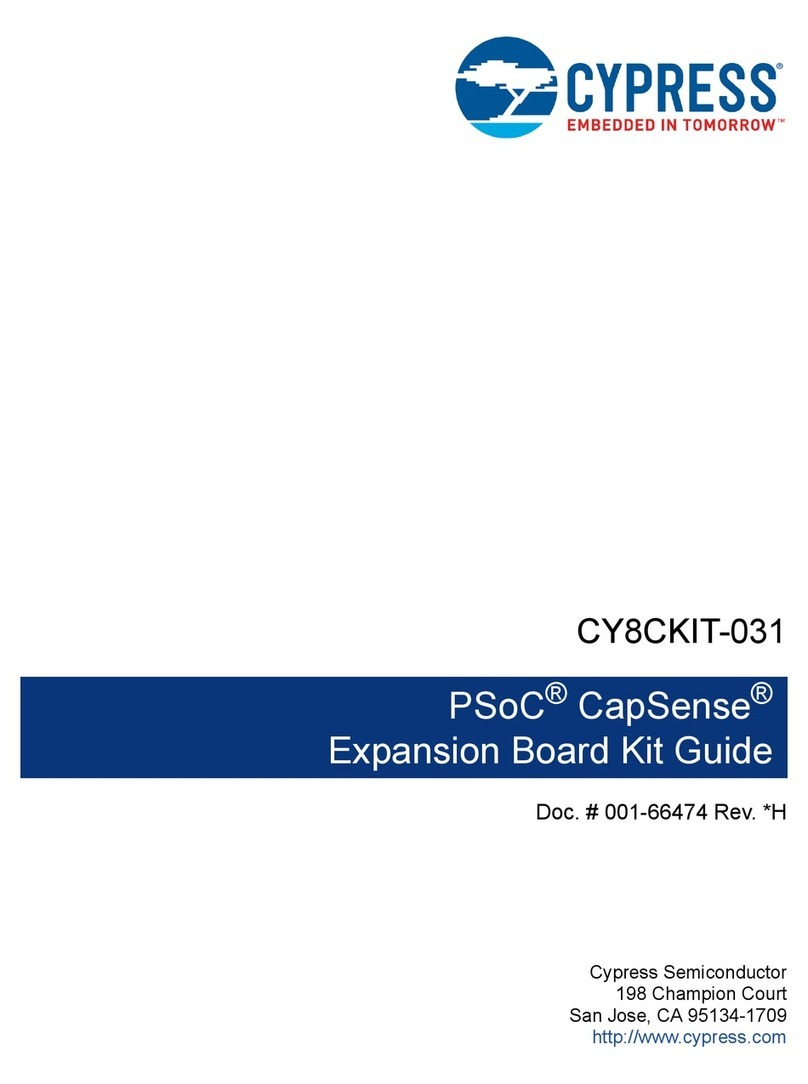
Cypress CY8CKIT-031 User manual
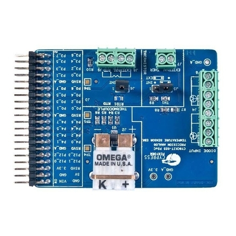
Cypress
Cypress CY8CKIT-025 User manual
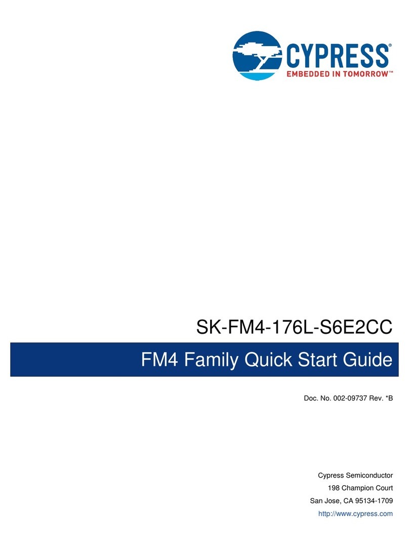
Cypress
Cypress SK-FM4-176L-S6E2CC User manual
Cypress
Cypress EZ-PD CCG3 User manual
Cypress
Cypress CY62128EV30 User manual
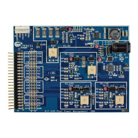
Cypress
Cypress CY8CKIT-035 User manual
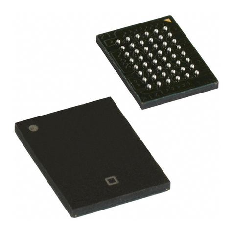
Cypress
Cypress EZ-OTG CY7C67200 User manual
Cypress
Cypress MB9B160R Series User manual
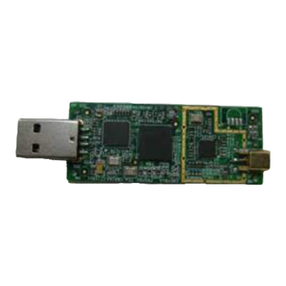
Cypress
Cypress FX2LP Guide

Cypress
Cypress MB2198-01 User manual
Cypress
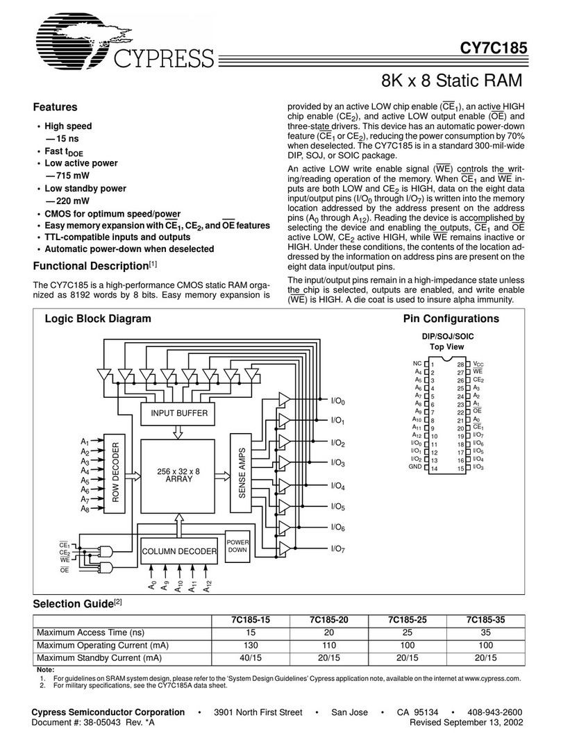
Cypress 7C185-15 User manual
Cypress
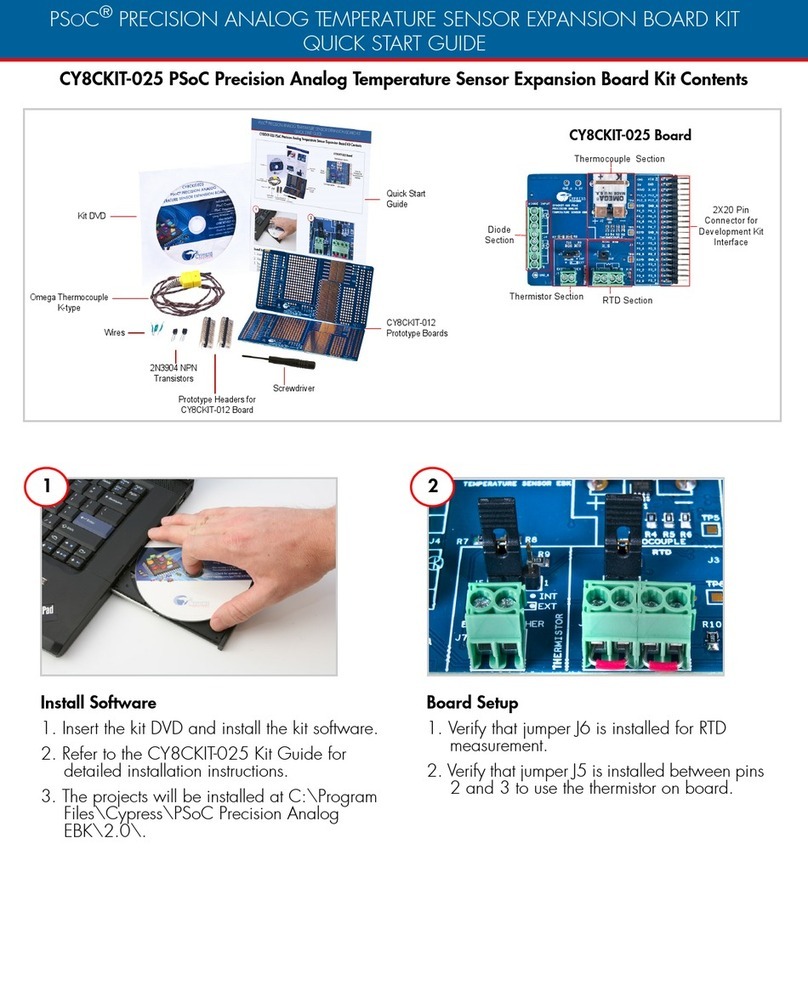
Cypress CY8CKIT-025 User manual
Cypress
Cypress CY91590 Series User manual
Cypress
Cypress AutoStore STK17T88 Installation and operating instructions
Cypress
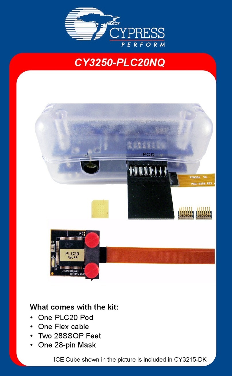
Cypress CY3250-PLC20NQ User manual
Cypress
Cypress CY62158EV30 User manual
Cypress
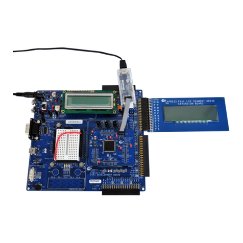
Cypress CY8CKIT-029 PSoC User manual
Cypress
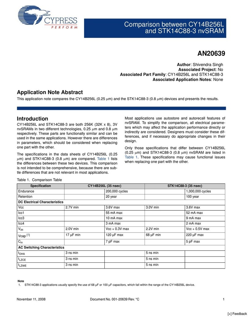
Cypress AN20639 Installation and operating instructions
Popular Computer Hardware manuals by other brands

EMC2
EMC2 VNX Series Hardware Information Guide

Panasonic
Panasonic DV0PM20105 Operation manual

Mitsubishi Electric
Mitsubishi Electric Q81BD-J61BT11 user manual

Gigabyte
Gigabyte B660M DS3H AX DDR4 user manual

Raidon
Raidon iT2300 Quick installation guide

National Instruments
National Instruments PXI-8186 user manual
