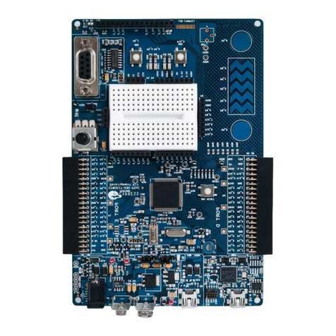
Cypress FR81S CY91F52 Series Operating instructions
Other Cypress Microcontroller manuals
Cypress
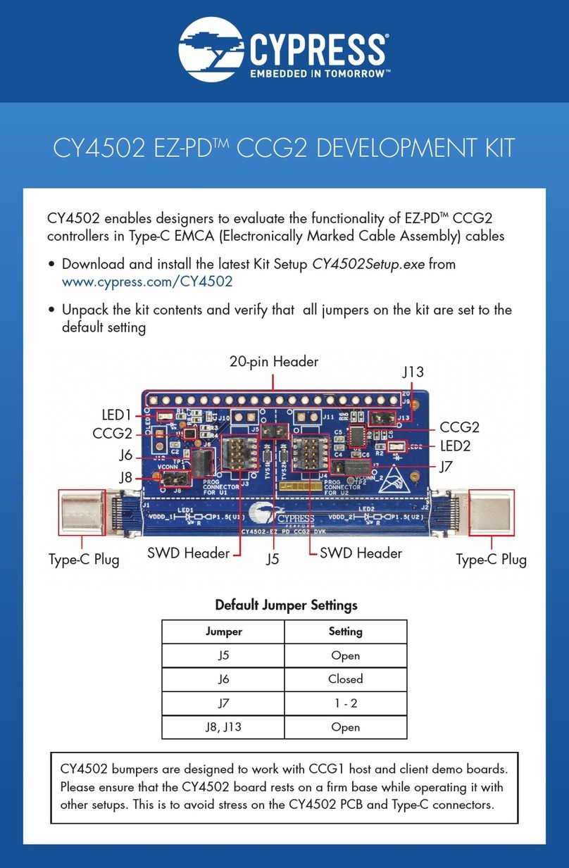
Cypress EZ-PD CY4502 User manual

Cypress
Cypress Traveo S6J3310 Series User manual
Cypress
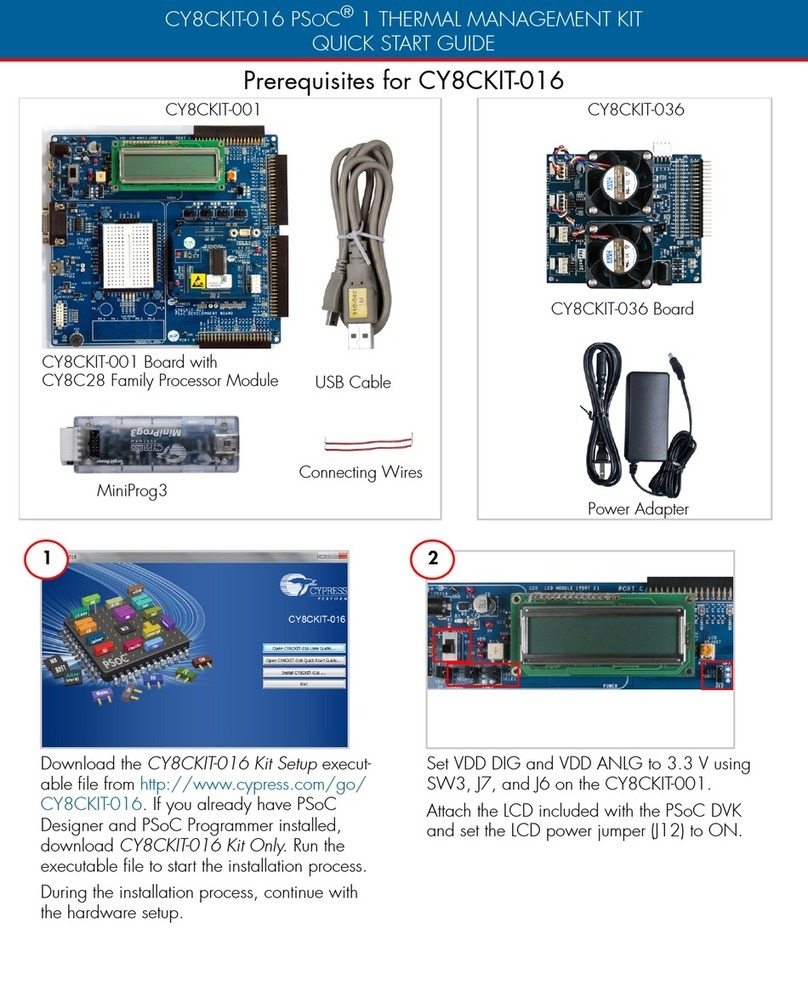
Cypress CY8CKIT-016 User manual

Cypress
Cypress PSOC 3 CY8CKIT-030A User manual
Cypress
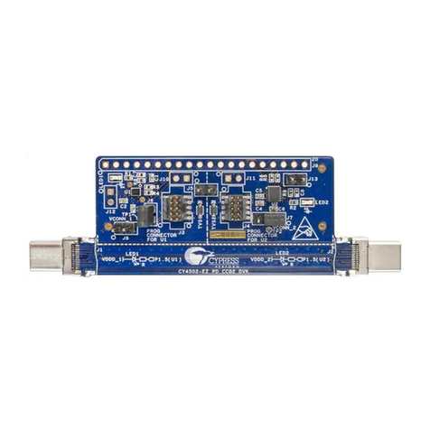
Cypress EZ-PD CY4502 User manual
Cypress
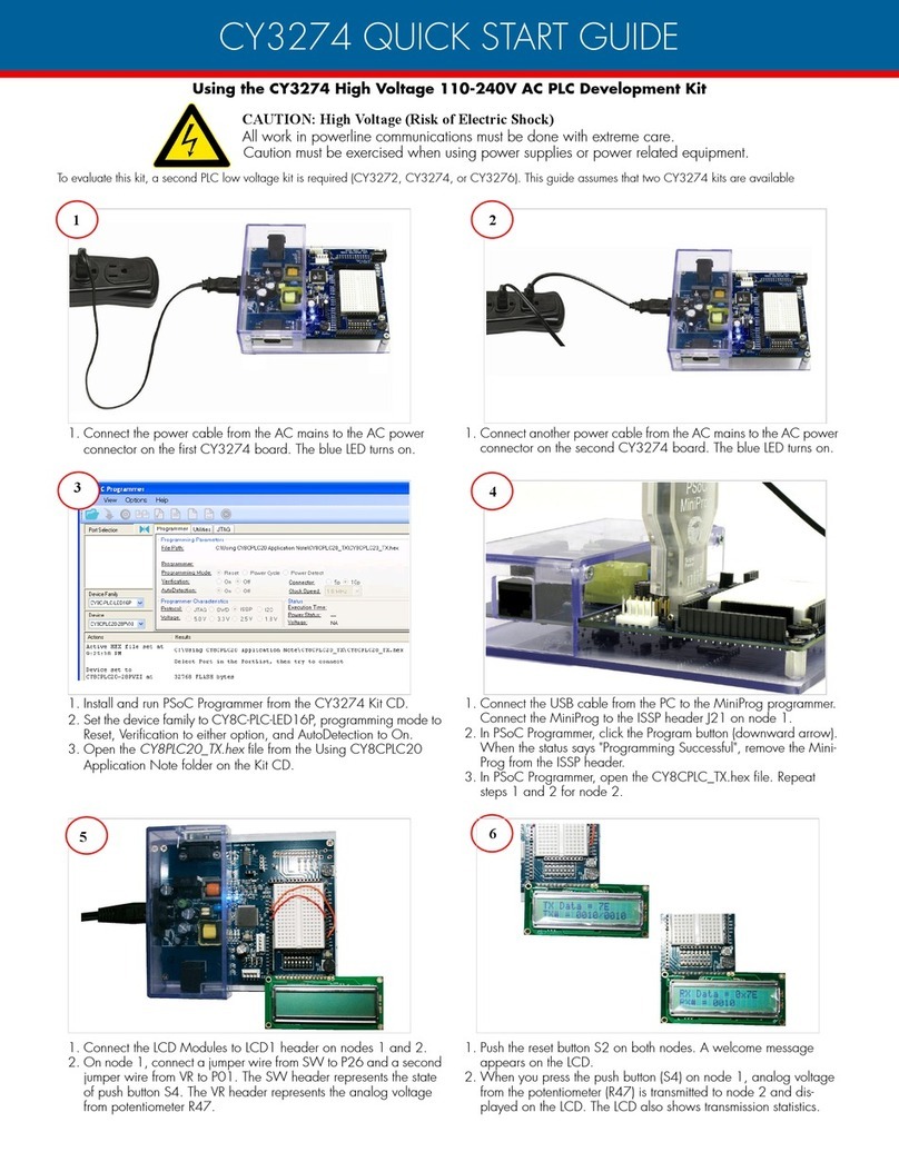
Cypress CY3274 User manual
Cypress
Cypress MB95310L Series User manual
Cypress
Cypress CY8CKIT-030 User manual

Cypress
Cypress S6J3200 Series Instruction Manual
Cypress
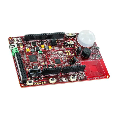
Cypress PSoC CY8CKIT-048 User manual
Cypress
Cypress MB90910 Series User manual
Cypress
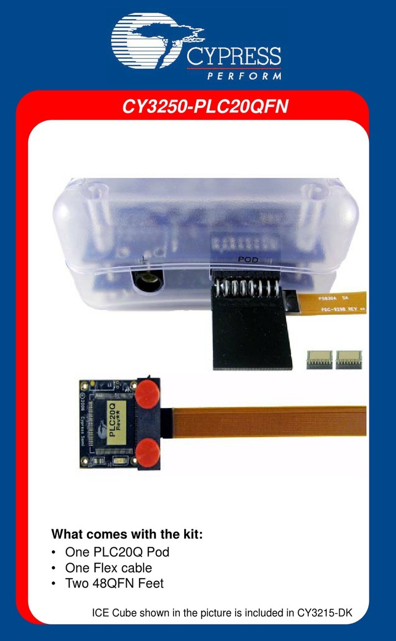
Cypress CY3250-PLC20QFN User manual
Cypress
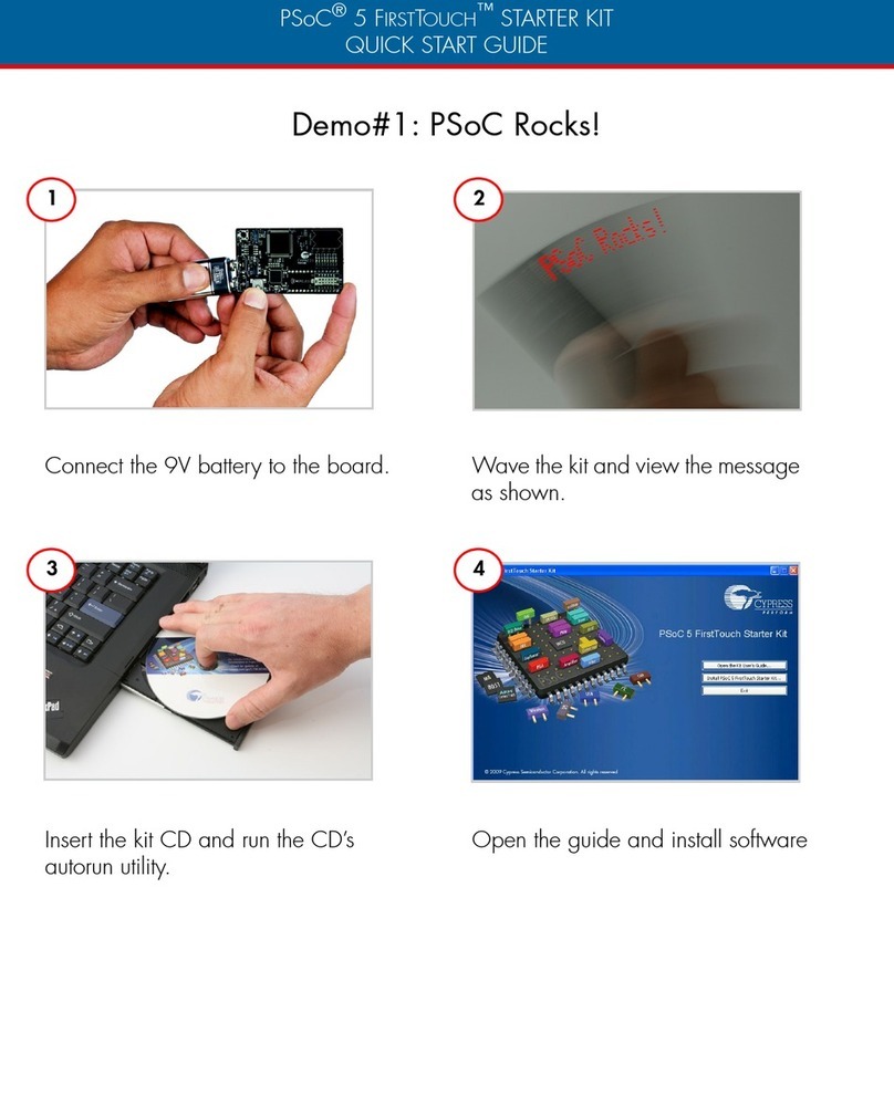
Cypress PSoC 5 FIRSTTOUCH CY8CKIT-014 User manual

Cypress
Cypress EZ-USB AT2LP CY4615B User manual
Cypress
Cypress S6E2CC Series User manual
Cypress
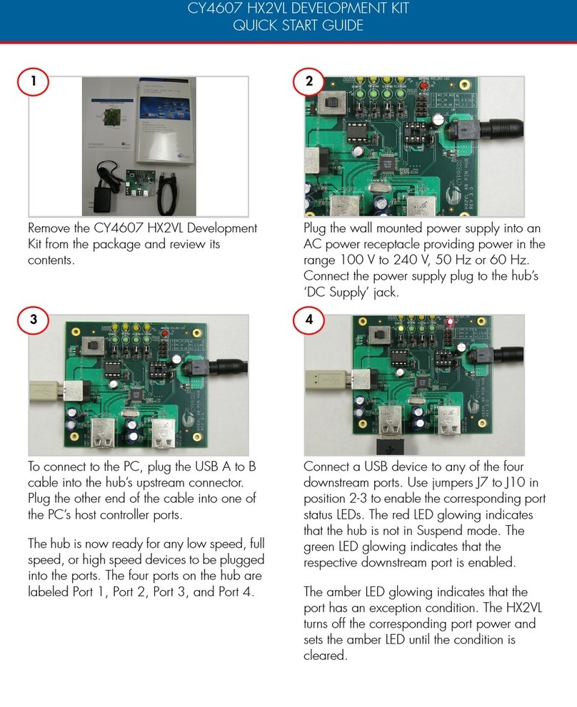
Cypress CY4607 HX2VL User manual
Cypress
Cypress CY3652 User manual
Cypress
Cypress PSoC 6 MCU Installation guide
Cypress
Cypress EZ-PD CY4502 User manual
Cypress
Cypress UNIVERSAL CAPSENS CY3280-BBM User manual
Popular Microcontroller manuals by other brands
AMS
AMS AS7261 Demo Kit user guide

Novatek
Novatek NT6861 manual
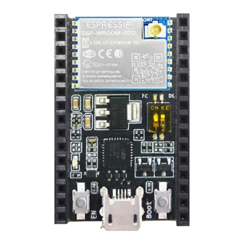
Espressif Systems
Espressif Systems ESP8266 SDK AT Instruction Set
Nuvoton
Nuvoton ISD61S00 ChipCorder Design guide
STMicrolectronics
STMicrolectronics ST7 Assembler Linker user manual
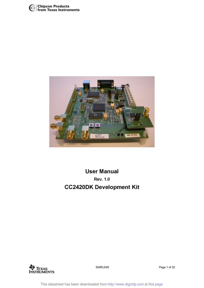
Texas Instruments
Texas Instruments Chipcon CC2420DK user manual
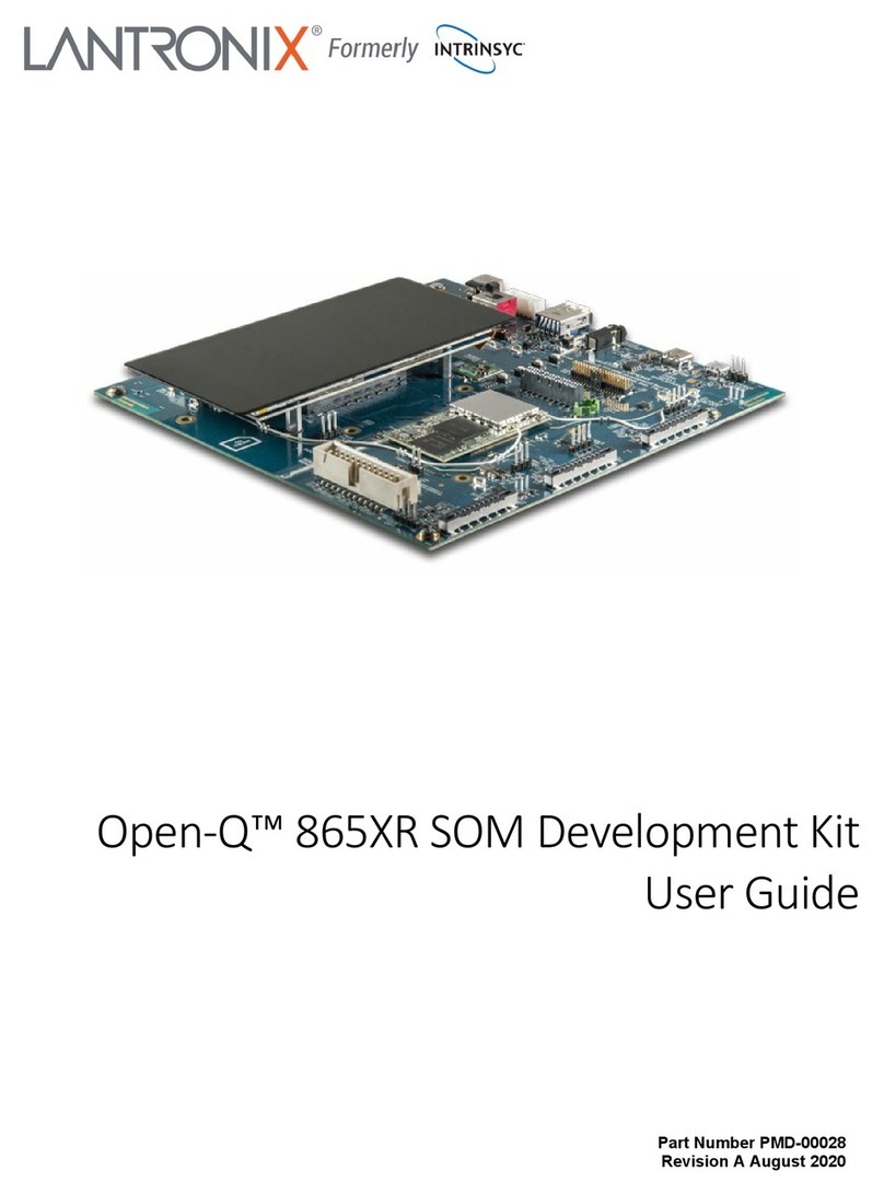
Lantronix
Lantronix Intrinsyc Open-Q 865XR SOM user guide

NEC
NEC 78GK0S/K 1+ Series Application note
Mikroe
Mikroe SEMITECH N-PLC Click Application note
Intel
Intel Agilex user guide
DIGITAL-LOGIC
DIGITAL-LOGIC MICROSPACE manual

Texas Instruments
Texas Instruments TMS320F2837 D Series Workshop Guide and Lab Manual

