NXP Semiconductors UM10741 User manual
Other NXP Semiconductors Microcontroller manuals
NXP Semiconductors
NXP Semiconductors MPC5777M User guide
NXP Semiconductors
NXP Semiconductors S12ZVML-MINIKIT User manual
NXP Semiconductors
NXP Semiconductors LPC800 User manual
NXP Semiconductors
NXP Semiconductors PN7462AU User manual
NXP Semiconductors
NXP Semiconductors LPC29 Series User manual
NXP Semiconductors
NXP Semiconductors Freescale TWR-POS-K81 User manual
NXP Semiconductors
NXP Semiconductors Kinetis KE1xZ256 User manual
NXP Semiconductors
NXP Semiconductors SLN-VIZNAS-IOT User manual
NXP Semiconductors
NXP Semiconductors IoT ZTB-DK006 User manual
NXP Semiconductors
NXP Semiconductors Freescale Xtrinsic LFSTBEB865X User manual
NXP Semiconductors
NXP Semiconductors Freescale Flexis MCF51MM256 User manual
NXP Semiconductors
NXP Semiconductors MPC5746R Guide
NXP Semiconductors
NXP Semiconductors LPC546 Series User manual
NXP Semiconductors
NXP Semiconductors A1006 User manual
NXP Semiconductors
NXP Semiconductors OM-SE051ARD User manual
NXP Semiconductors
NXP Semiconductors OM2NTA5KIT User manual
NXP Semiconductors
NXP Semiconductors LPC-Link2 Quick start guide
NXP Semiconductors
NXP Semiconductors KE1xF Series User manual
NXP Semiconductors
NXP Semiconductors S32G-VNP-GLDBOX User manual
NXP Semiconductors
NXP Semiconductors A71CLARD-BA User manual
Popular Microcontroller manuals by other brands

Novatek
Novatek NT6861 manual
Espressif Systems
Espressif Systems ESP8266 SDK AT Instruction Set
Nuvoton
Nuvoton ISD61S00 ChipCorder Design guide
STMicrolectronics
STMicrolectronics ST7 Assembler Linker user manual
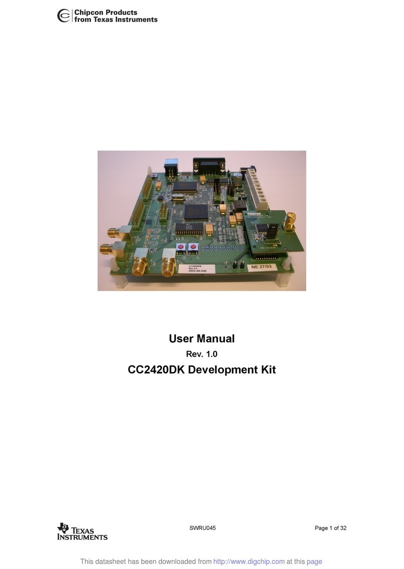
Texas Instruments
Texas Instruments Chipcon CC2420DK user manual
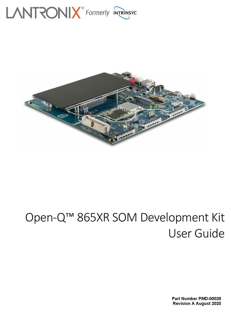
Lantronix
Lantronix Intrinsyc Open-Q 865XR SOM user guide

