e2v AT84AS003-EB User manual

AT84AS003-EB Evaluation Board
..............................................................................................
User Guide


Table of Contents
AT84AS003-EB Evaluation Board User Guide i
0905C–BDC–09/07
Section 1
Introduction ........................................................................................... 1-1
1.1 Scope........................................................................................................1-1
1.2 Description ................................................................................................1-1
Section 2
Hardware Description ........................................................................... 2-1
2.1 Board Structure.........................................................................................2-1
2.2 Analog Inputs/Clock Inputs .......................................................................2-2
2.3 Digital Outputs ..........................................................................................2-3
Section 3
Operating Characteristics ..................................................................... 3-1
3.1 Introduction ...............................................................................................3-1
3.2 Operating Procedure.................................................................................3-1
Section 4
Application Information ......................................................................... 4-1
4.1 Introduction ...............................................................................................4-1
4.2 Analog Inputs ............................................................................................4-1
4.3 Clock Inputs ..............................................................................................4-1
4.4 Digital Outputs ..........................................................................................4-1
4.5 ADC Functions..........................................................................................4-2
4.6 DMUX Function.........................................................................................4-4
4.7 Diode for Die Junction Temperature Monitoring .......................................4-7
4.8 Test Bench Description...........................................................................4-10
Section 5
Package Information............................................................................. 5-1
5.1 Thermal Characteristics ............................................................................5-1
Section 6
Ordering Information............................................................................. 6-1
Section 7
Appendix............................................................................................... 7-1
7.1 AT84AS003-EB Electrical Schematics .....................................................7-1

ii AT84AS003-EB Evaluation Board User Guide
0905C–BDC–09/07

AT84AS0003-EB Evaluation Kit User Guide 1-1
0905C–BDC–09/07
Section 1
Introduction
1.1 Scope
The AT84AS003-EB Evaluation Kit is designed to facilitate the evaluation and charac-
terization of the AT84AS003 10-bit 1.5 Gsps ADC with 1:2/4 DMUX up to its 3 GHz full
power input bandwidth and up to 1.5 Gsps.
The AT84AS003-EB Evaluation Kit includes:
The 10-bit 1.5 Gsps ADC with 1:2/4 DMUX Evaluation board including the
AT84AS003 device soldered and a heat sink screwed on the board
10 SMA caps for CLK, CLKN, VIN, VINN, DAI, DAIN, DAO, DAON, DRRB and
AsyncRST signals
12 jumpers for ADC and DMUX function settings (SDAEN, B/GB, PGEB, RS, BIST,
CLKTYPE, DRTYPE, SLEEP, STAGG, DAEN)
The user guide uses the AT84AS003-EB Evaluation Kit as an evaluation and demon-
stration platform and provides guidelines for its proper use.
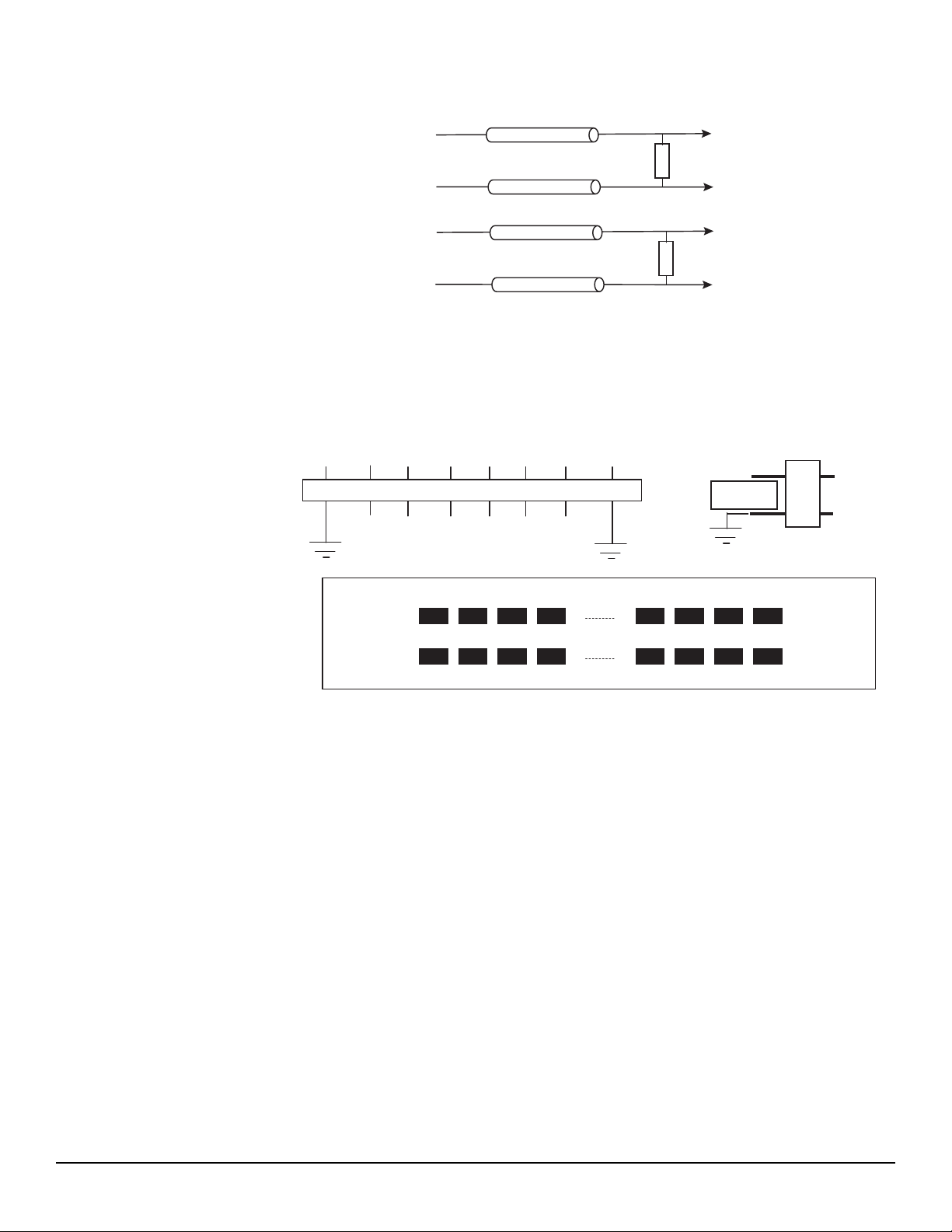
1.2 Description
The AT83AS003-EB evaluation board is very straightforward as it only implements the
AT84AS003 10-bit 1.5 Gsps ADC/DMUX device, SMA connectors for the sampling
clock, analog inputs and reset inputs accesses and 2.54 mm pitch connectors compati-
ble with high-speed acquisition system probes.
To achieve optimal performance, the AT84AS003-EB evaluation board was designed in
a 8-metal-layer board with RO4003 200 µm and FR4 HTG epoxy dielectric materials.
The board implements the following devices:
The 10-bit 1.5 Gsps ADC with 1:2/4 DMUX evaluation board with the AT84AS003
ADC soldered and a heat sink screwed on the board
10 SMA caps for CLK, CLKN, VIN, VINN, DAI, DAIN, DAO, DAON, DRRB and
AsyncRST signals
12 jumpers for ADC and DMUX function settings (SDAEN, B/GB, PGEB, RS, BIST,
CLKTYPE, DRTYPE, SLEEP, STAGG, DAEN)
2.54 mm pitch connectors for the digital outputs, compatible with high speed
acquisition system probes
Banana jacks for the power supply accesses and the die junction temperature
monitoring functions (2 mm)

Introduction
1-2 AT84AS0003-EB Evaluation Kit User Guide
0905C–BDC–09/07
Potentiometers for the ADC and DMUX functions
The board is comprised of 8 metal layers for signal traces, ground and power supply lay-
ers, and 7 dielectric layers featuring low insertion loss and enhanced thermal
characteristics for operation in the high frequency domain.
The board dimensions are 220 mm × 240 mm.
The board comes fully assembled and tested, with the AT84AS003 installed and with a
heat sink.
Figure 1-1. Simplified Schematics of the AT84AS003-EB Evaluation Board
As shown in Figure 1-1, different power supplies are required:
V
EE
= -5V analog negative power supply
V
MINUSD
= -2.2V digital negative power supply
V
CCA
= 3.3V analog positive power supply
V
CCD
= 3.3V digital positive power supply
V
PLUSD
= 2.5V digital output power supply
3.3V and -5V power supplies for the board functions
DACTRL
PIN 1
Port D
Port C
GA
SDAEN
Port B
Port A
DMUX functions
CLK
CLKN
VINN
VIN
ASYNCRST
DDRB
3.3V -5V
GND
Diode
ADC functions
CLKDACTRL
DAO/DAON
G
N
D
G
N
D
G
N
D
G
N
D
DR
DAI/DAIN
AT84AS003
G
N
D
V
E
E
V
M
I
N
U
S
D
V
C
C
A
V
C
C
D
V
+
D

AT84AS003-EB Evaluation Kit User Guide 2-1
0905C–BDC–09/07
Section 2
Hardware Description
2.1 Board Structure
In order to achieve optimum full-speed operation of the AT84AS003 10-bit 1.5 Gsps
ADC with 1:2/4 DMUX, a multi-layer board structure was retained for the evaluation
board. Eight copper layers are used, respectively dedicated to the signal traces, ground
planes, power supply planes and DC signals traces.
The board is made in RO4003 200 µm and FR4 HTG epoxy dielectric materials.
The following table gives a detailed description of the board's structure.
Table 2-1. Board Layer Thickness Profile
Layer Characteristics
Layer 1
Copper layer
Copper thickness = 40 µm
AC signals traces = 50Ωmicrostrip lines
DC signals traces (B/GB, GA, ADC Diode,
SDA)
Layer 2
RO4003 dielectric layer
(Hydrocarbon/wovenglass)
Layer thickness = 200 µm
Dielectric constant = 3.4 at 10 GHz
-0.044 dB/inch insertion loss at 2.5 GHz
-0.318 dB/inch insertion loss at 18 GHz
Layer 3
Copper layer
Copper thickness = 35 µm
Upper ground plane = reference plane 50Ω
microstrip return
Layer 4
FR4 HTG/dielectric layer Layer thickness = 170 µm
Layer 5
Copper layer
Copper thickness = 35 µm
Power planes = V
CCA
and V
CCD
Layer 6
FR4 HTG/dielectric layer Layer thickness = 200 µm
Layer 7
Copper layer
Copper thickness = 35 µm
Power planes = VEE and 3.3V
Layer 8
FR4 HTG/dielectric layer Layer thickness = 170 µm

Hardware Description
2-2 AT84AS003-EB Evaluation Kit User Guide
0905C–BDC–09/07
The board is 1.6 mm thick.
The clock, analog input, reset and digital data output signals occupy the top metal layer
while the ADC and DMUX functions are located on both the top layer and the 15th layer.
The ground planes occupy layer 3, 13 and 15 (partly).
Layer 5, 7, 9 and 11 are dedicated to the power supplies.
2.2 Analog
Inputs/Clock
Inputs
The differential active inputs (clock, analog, DAI/DAIN, DRRB and ASYNCRST) are pro-
vided by SMA connectors.
Reference: VITELEC 142-0701-8511
Special care was taken for the routing of the analog input, clock input and DAI/DAIN sig-
nals for optimum performance in the high frequency domain:
50Ωlines matched to ±0.1 mm (in length) between VIN and VINN
50 mm max line length
1.27 mm pitch between the differential traces
400 µm line width
40 µm thickness
850 µm diameter hole in the ground layer below the VIN and VINN ball footprints
Layer 9
Copper layer
Copper thickness = 35 µm
Power planes = V
PLUSD
Layer 10
FR4 HTG/dielectric layer Layer thickness = 200 µm
Layer 11
Copper layer
Copper thickness = 35 µm
Power planes = VMINUSD, -5V
Layer 12
FR4 HTG/dielectric layer Layer thickness = 170 µm
Layer 13
Copper layer
Copper thickness = 35 µm
Ground plane = reference plane (identical to
layer 3)
Layer 14FR4 HTG/dielectric layer Layer thickness = 200 µm
Layer 15
Copper layer
Copper thickness = 40 µm
DC signals traces (B/GB, GA, Diode, SDA)
Ground plane
Table 2-1. Board Layer Thickness Profile (Continued)
Layer Characteristics

Hardware Description
AT84AS003-EB Evaluation Kit User Guide 2-3
0905C–BDC–09/07
Figure 2-1. Board Layout for the Differential Analog, Clock and DAI/DAIN Inputs
Note: The analog inputs are reverse terminated with 50Ωto ground very close to the
device (same line length used for both reverse termination).
Figure 2-2. Differential Analog Inputs Implementation
2.3 Digital Outputs
The digital output lines were designed with the following recommendations:
50Ωlines matched to ± 0.5 mm (in length) between signal of the same differential pair
80 mm max line length
±1 mm line length difference between signals of two ports
±1.5 mm max line length difference between all signals
770 µm pitch between the differential traces
370 µm line width
40 µm thickness
Figure 2-3. Board Layout for the Differential Digital Outputs
The digital outputs are compatible with LVDS standard. They are on-board 100Ωdiffer-
entially terminated as shown in Figure 2-4 on page 2-4.
200 µm
RO4003
400 µm 870 µm
1270 µm
Ground plane
400
µm
e = 40 µm
VIN (W24)
VINN
(W23)
VIN (V25)
50Ω
GND
50Ω
GND VINN (V22)
VIN
VINN
AT84AS003
200 µm
RO4003
µm 400 µm
µm
Ground plane
370
µm
e = 40 µm
370
770

Hardware Description
2-4 AT84AS003-EB Evaluation Kit User Guide
0905C–BDC–09/07
Figure 2-4. Differential Digital Outputs Implementation
Double row 2.54 mm pitch connectors are used for the digital output data. The upper
row is connected to the signal while the lower row is connected to Ground, as illustrated
in Figure 2-5
Figure 2-5. Differential Digital Clock Outputs 2.54 mm Pitch Connector
(Example Port A)
Di
DiN
100Ω
50Ω
Line
50
ΩLine
DRN
DR
100Ω
50
ΩLine
50
ΩLine
A0N A0 AORN
/DR A
AOR
/DRA N
…
Ground
Signal
GND A0N A0 A1N AORN AOR GND B0
GND GND GND GND GND GND GND GND

AT84AS003-EB Evaluation Kit User Guide 3-1
0905C–BDC–09/07
Section 3
Operating Characteristics
3.1 Introduction
This section describes a typical configuration for operating the evaluation board of the
AT84AS003 10-bit 1.5 Gsps ADC with 1:2/4 DMUX.
The analog input signal and the sampling clock signal can be accessed either in differ-
ential or single-ended fashion.
The single-ended configuration is the most straightforward but it is recommended to
work in differential mode (especially for the clock signal) for frequencies above 1 GHz.
In the case of use in differential mode, the AT84AS003 clock inputs have to be fed with
balanced signals (use a balun or Hybrid junction to convert a single signal to a differen-
tial signal).
In the case of use in single-ended mode, the inverted analog input V
INN
and clock input
CLKN should be terminated properly with 50Ωto ground (50Ωcaps can be used to ter-
minate the SMA connectors).
The RF sources can then be connected directly to the ADC's in-phase analog and clock
inputs.
3.2 Operating
Procedure
1. Connect the power supplies and ground accesses through the dedicated banana
jacks.V
EE
= -5V, V
MINUSD
= -2.2V, V
CCA
= 3.3V, V
CCD
= 3.3V, V
PLUSD
= 2.5V, 3.3V
and -5V
V
CCD
= 3.3V and 3.3V and V
EE
= -5V and -5V have separated planes but can be
reunited via a short-circuit available on the top metal layer.
2. Connect the clock input signals. In single-ended mode, terminate the inverted
phase signal (CLKN) to a 50Ωtermination to ground (50Ωcap).Use a low-phase
noise High Frequency generator.The clock input level is typically 0 dBm and
should not exceed 4 dBm (into 50Ω).The clock frequency can range from 150
MHz up to 1.5 GHz.
3. Connect the analog input signal. In single-ended mode, VINN should be termi-
nated by 50Ωto ground (50Ωcap).Use a low-phase noise High Frequency
generator. The analog input full-scale is 500 mV peak-to-peak around
0V (± 250 mV). It is recommended to use the ADC with an input signal of -1
dBFS max (to avoid saturation of the ADC). The analog input frequency can
range from DC up to 1.8 GHz. At 3 GHz, the ADC attenuates the input signal by
3 dB.
4. Connect the high-speed acquisition system probes to the output connectors.

Operating Characteristics
3-2 AT84AS003-EB Evaluation Kit User Guide
0905C–BDC–09/07
The digital data are differentially terminated on-board (100Ω) however, they can be
probed either in differential or in single-ended mode.
5. Connect the ADC and DMUX function jumpers.
All instrumentation and connectors are now connected.
6. Switch on the power supplies (recommended power up sequence: simultaneous
or in the following order: V
EE
= -5V and -5V, then V
MINUSD
= -2.2V, and finally
V
CCA
= 3.3V, V
CCD
= 3.3V, 3.3V and V
PLUSD
= 2.5V).
7. Switch on the RF clock generator.
8. Switch on the RF signal generator.
9. Perform an asynchronous reset (ASYNCRST push button) on the device.
The AT84AS003-EB evaluation board is now ready for operation
Note: 1. Absolute maximum ratings are short term limiting values (referenced to GND = 0 V), to be applied individually, while other
parameters are within specified operating conditions. Long exposure to maximum ratings may affect device reliability.
2. All integrated circuits have to be handled with appropriate care to avoid damage due to ESD. Damage caused by inappropri-
ate handling or storage could range from performance degradation to complete failure
Table 3-1. Absolute Maximum Ratings
Parameter Symbol Value Unit
Analog positive supply voltage V
CCA
GND to 6 V
Digital positive supply voltage V
CCD
GND to 3.6 V
Analog negative supply voltage V
EE
GND to -5.5 V
Digital positive supply voltage V
PLUSD
GND to 3 V
Digital negative supply voltage V
MINUSD
GND to -3 V
Maximum difference between
V
PLUSD
and V
MINUSD
V
PLUSD
- V
MINUSD
5V
Analog input voltages V
IN
or V
INN
-1.5 to 1.5 V
Maximum difference between
V
IN
and V
INN
V
IN
or V
INN
-1.5 to 1.5
Clock input voltage V
CLK
or V
CLKN
-1 to 1 V
Maximum difference between
V
CLK
and V
CLKN
V
CLK
- V
CLKN
-1 to 1 Vpp
Control input voltage GA, SDAEN -5 to 0.8 V
Digital input voltage SDAEN, B/GB, PGEB, DECB -5 to 0.8 V
ADC reset voltage DRRB -5 to 0.8 V
DMUX function input voltage RS, CLKTYPE, DRTYPE, SLEEP,
STAGG, BIST, DAEN -0.3 to V
CCD
+ 0.3 V
DMUX Asynchronous Reset ASYNCRST -0.3 to V
CCD
+ 0.3
DMUX input Voltage DAI, DAIN -0.3 to V
CCD
+ 0.3 V
DMUX control Voltage CLKDACTRL, DACTRL -0.3 to V
CCD
+ 0.3 V
Maximum input voltage on DIODE DIODE ADC 700 mV
Maximum input current on DIODE DIODE ADC 1 mA
Junction temperature T
J
135 °C

Operating Characteristics
AT84AS003-EB Evaluation Kit User Guide 3-3
0905C–BDC–09/07
Table 3-2. Operating Characteristics Ambient Temperature (V
CCA
= V
CCD
= 3.3V, V
EE
= -5V, V
MINUSD
= -2.2V;
V
PLUSD
= 2.5V; V
INN
- V
INN
= 1 dBFS, P
CLK
= 0 dBm Differential
Parameter Symbol Min Typ Max Unit
Resolution 10 Bit
Power Requirements
Positive supply voltage
- Analog
- Digital
- Output V
CCD
V
CCA
V
CCD
V
PLUSD
3.15
3.15
2.4
3.3
3.3
2.5
3.45
3.45
2.6
V
V
V
Positive supply current
- Analog
V
CCA
- Digital V
CCD
1:2 DMUX
- Digital V
CCD
1:4 DMUX
- Output V
CCD
I
VCCA
I
VCCD
I
VCCD
I
VPLUSD
80
535
565
450
100
590
620
470
mA
mA
mA
mA
Negative supply voltage V
EE
-5.25 -5 -4.75 V
Negative supply current I
VEE
620 660 mA
Negative supply voltage V
MINUSD
-2.3 -2.2 -2.1 V
Negative supply current V
MINUSD
190 200 mA
Power Dissipation (1:2 DMUX) PD 6.5 7.1 W
Analog Inputs
Full-scale input voltage range (differential
mode)
(0V common mode voltage)
V
IN
V
INN
-125
-125
125
125
mV
mV
Full-scale input voltage range (single-
ended input option) (0V common mode
voltage)
V
IN
, V
INN
-250 0 250 mV
Analog input power level
(50Ωsingle-ended) P
IN
-2 dBm
Analog input capacitance (die) C
IN
0.3 pF
Input leakage current I
IN
10 µA
Input resistance
- Single-ended
- Differential
R
IN
R
IN
49
98
50
100
51
102
Ω
Ω
Clock Inputs
Logic common mode
compatibility for clock inputs
Differential ECL to LVDS
(AC coupling)

Operating Characteristics
3-4 AT84AS003-EB Evaluation Kit User Guide
0905C–BDC–09/07
Clock input common voltage range
(V
CLK
or V
CLKN
)
(DC coupled clock input)
V
CM
-1.2 0 3.3 V
Clock input power level (low-phase noise
sinewave input) 50Ωsingle-ended or
100Ωdifferential
P
CLK
-4 0 4 dBm
Clock input swing (single ended; with
CLKN = 50Ωto GND) V
CLK
±200 ±320 ±500 mV
Clock input swing (differential voltage) on
each clock input V
CLK
, V
CLKN
±141 ±226 ±354 mV
Clock input capacitance (die) C
LK
0.3 pF
Clock input resistance
- Single-ended
- Differential ended
R
CLK
R
CLK
45
90
50
100
55
110
Ω
Ω
Digital Data Outputs
Logic compatibility LVDS
50Ωtransmission lines, 100Ω(2 × 50Ω
differential termination)
- Logic low
- Logic high
- Differential output
- Common mode
V
OL
V
OH
V
ODIFF
V
OCM
–
1.25
250
1.125
1.075
1.425
350
1.25
1.25
–
450
1.375
V
V
mV
V
Control Function Inputs
DRRB and ASYNCRST
- Logic low
- Logic high
- Common
V
IL
V
IH
V
ICM
0
1.6
1.4
1
3.3
V
V
V
RS, DRTYPE, SLEEP, STAGG, BIST,
DAEN
- Logic low
- Logic high
R
IL
R
IH
0
10 K
10
Infinite
Ω
Ω
SDAEN, PGEB, B/GB
- Logic low
- Logic high -2
V
EE
0
-3
0
V
V
DAI, DAIN
Differential Input
common mode
V
IDIFF
V
ICM
1
100
1.25
350
1.6
–
V
mV
GA, SDA -0.5 0.5 V
CLKDACTRL, DACTRL 1/3 × V
CCD
1/3 × V
CCD
2/3 × V
CCD
V
Table 3-2. Operating Characteristics Ambient Temperature (V
CCA
= V
CCD
= 3.3V, V
EE
= -5V, V
MINUSD
= -2.2V;
V
PLUSD
= 2.5V; V
INN
- V
INN
= 1 dBFS, P
CLK
= 0 dBm Differential (Continued)
Parameter Symbol Min Typ Max Unit

AT84AS003-EB Evaluation Kit User Guide 4-1
0905C–BDC–09/07
Section 4
Application Information
4.1 Introduction
For this section, refer also to the product “Main features” section of the AT84AS003
datasheet ref 0808.
4.2 Analog Inputs
The analog inputs can be entered in differential or in single-ended mode but a differen-
tial mode is recommended using a balun or hybrid junction.
In single-ended mode, the unused input signal SMA connector should be terminated
with a 50Ωcap to provide proper termination of the differential pair.
It is recommended that a filter be used to optimize the dynamic performance and the
spectral response of the ADC.
4.3 Clock Inputs
The clock inputs can be entered in differential or in single-ended mode without any high
speed performance degradation for a clock frequency up to 1 GHz. At higher rates, it is
recommended to drive the clock inputs differentially using a balun or hybrid junction.
In single-ended mode, the unused clock input signal SMA connector should be termi-
nated with a 50Ωcap to provide proper termination of the differential pair.
The clock can be supplied with a sinewave signal centered on 0V common mode.
4.4 Digital Outputs
The digital outputs (data and Data Ready) are LVDS compatible. 100Ωdifferential termi-
nation is provided on-board.

Application Information
4-2 AT84AS003-EB Evaluation Kit User Guide
0905C–BDC–09/07
Figure 4-1. Differential Digital Outputs Implementation
4.5 ADC Functions
4.5.1 Data Ready Reset The Data Ready reset signal is accessed via an SMA connector.
DRRB is CMOS/LVCMOS compatible:
VIL = 0 (typical)
VIH = V
CCA
(typical)
This signal acts as an internal reset of the device. It is not mandatory for proper opera-
tion of the device. It is only used to determine exactly the first data to be sampled.
When applied, the clock outputs are reset. The reset pulse should last at least 1 ns.
An asynchronous reset (ASYNCRST push button) should be applied while DRRB is
active (low) in order to reset properly the whole device.
In most cases (single channel application, no need to know which data will be the first
one to be sampled), this reset can be left unused.
4.5.2 Binary or Gray
Output Coding
One jumper is used to set the ADC output coding mode in either Binary or Gray:
Binary coding: connect the jumper to ground
Gray coding: connect the jumper to the upper position (see Figure 4-2)
Figure 4-2. Binary or Gray coding Jumper Position
Di
DiN
DRN
DR
100Ω
50Ω Line
50Ω Line
50Ω Line
50Ω Line
100Ω
GND
GND
B/GB
B/GB
Binary
Coding
Gray
Coding

Application Information
AT84AS003-EB Evaluation Kit User Guide 4-3
0905C–BDC–09/07
4.5.3 Gain Adjust The ADC gain can be adjusted by the means of the GA potentiometer (varying from -
0.5V to 0.5V around 0V nominal value). A GA jumper is available to allow or disable this
function.
When connected to ground, the Gain adjustment is disabled. In the other position, the
user can tune the ADC gain by varying the GA potentiometer.
The GA potentiometer allows you to tune the Gain from approximately 0.85 to 1.15.
Figure 4-3. ADC Gain Adjust Jumper Settings
Figure 4-4. The ADC Gain Adjust Function is given in Figure 4.4
4.5.4 Sampling Delay
Adjust The SDA function (Sampling delay adjust) allows to fine tune the sampling ADC aper-
ture delay TA around its nominal value (160 ps). This functionality is enabled thanks to
the SDAEN signal, which is inactive when its associated jumper is connected to GND, or
active in the other position
GND
GND
GA
GA
No Gain
Ad
j
ustment
Gain Adjustmen
t
Allowed
0,50
0,60
0,70
0,80
0,90
1,00
1,10
1,20
1,30
-0,5 -0,4 -0,3 -0,2 -0,1 0 0,1 0,2 0,3 0,4 0,5
VGA Gain Adjust Voltage (V)
ADC Gai
n
min
typical

Application Information
4-4 AT84AS003-EB Evaluation Kit User Guide
0905C–BDC–09/07
Figure 4-5. DC SDAEN Jumper Settings
The variation of the delay around its nominal value as function of SDA voltage is shown
in Figure 4-6 on page 4-4.
The typical tuning range is ±120 ps for an applied control voltage varying between
-0.5 V to 0.5 V on SDA potentiometer. The variation of the delay in function of the tem-
perature is negligible.
Figure 4-6. SDA Transfer Functions
4.5.5 Pattern Generator The AT84AS003 is able to generate by itself (no need of analog input signal) a series of
patterns made of 10-bit transitioning from 0 to 1 or 1 to 0.
At the AT84AS003 output, all bits of each port are all 1 or all 0 and do not transition
every cycle (all bits of all ports remain the same: that is, if port A = 1010101010, then at
next cycle, port A = 1010101010). Ports A and C output the same data, ports B and D
output the inverted data compared to ports A and D.
This pattern generator can be used to test the ADC part of the device (a BIST is avail-
able for the testing of the DMUX part of the device).
One jumper is used to set the ADC in this Test mode:
Pattern Generator inactive: connect the jumper to ground
Pattern Generator active: connect the jumper to the upper position (see Figure 4-3 on
page 4-3)
GND GND
SDAEN
SDAEN
SDA Allowed
SDA Disabled
100p
200p
300p
-500m
-400m -300m -200m -100m -0.00 100m 200m 300m 400m 500m
Delay in the variable cell at 60C
sda

Application Information
AT84AS003-EB Evaluation Kit User Guide 4-5
0905C–BDC–09/07
Figure 4-7. Pattern Generator Enable Jumper Position
4.6 DMUX Function
4.6.1 ASYNCRST The asynchronous reset is mandatory to start the device properly. It must be applied
after power up of the device.
A push button is provided to perform this reset and pull-up and pull-down resistors allow
to keep the ASYNCRST signal inactive.
Figure 4-8. Reset Function
If the DRRB reset is also used, it is recommended to apply the asynchronous reset while
the DRRB reset is active.
The first data is available at the device output after TOD + 7.5 cycles.
4.6.2 CLKDACTRL A delay cell is provided to allow you to tune the delay between the clock and data at the
DMUX input. The delay is controlled via the CLKDACTRL potentiometer.
This cell allows you to delay by ±250 ps (around 250 ps) the internal DMUX clock via the
CLKDACTRL potentiometer (varying from V
CCD
/3 to (2 × V
CCD
)/3).
GND GND
PGEB
PGEB
Pattern Generator Pattern Generator
Active
Inactive
3.3V
GND
3.3V
15K
4.7K
AT84AS003

Application Information
4-6 AT84AS003-EB Evaluation Kit User Guide
0905C–BDC–09/07
Figure 4-9. CLKDACTRL Function
4.6.3 DACTRL A standalone delay cell is available (Input = DAI/DAIN, output DAO/DAON, control =
DACTRL, Enable = DAEN).
This cell allows you to delay by ±250 ps (around 250 ps) the incoming signal DAI/DAIN
via the DACTRL potentiometer (varying from V
CCD
/3 to (2 × V
CCD
)/3).
Figure 4-10. DACTRL Funtion
4.6.4 RS, DRTYPE, DAEN,
BIST, CLKTYPE,
SLEEP, STAGG
Seven Jumpers are provided for the RS, DRTYPE, DAEN, BIST, CLKTYPE, SLEEP
and STAGG functions.
3.3V
10 KΩ
10 KΩ
10 KΩ
GND
AT84AS003
3.3V
10 KΩ
10 KΩ
10 KΩ
GND
AT84AS003
Table of contents
Other e2v Motherboard manuals