e2v EV10AS150A User manual

ADC EV10AS150A Evaluation Board
User Guide

2ADC EV10AS150A User Guide
0977B–BDC–09/09

EV10AS150A-EB User Guide 1
0977B–BDC–10/09
Table of Contents
Section 1
Introduction ........................................................................................... 1-1
1.1 Scope1-1
1.2 Description ................................................................................................1-1
Section 2
Hardware Description ........................................................................... 2-1
2.1 Board Structure.........................................................................................2-1
2.2 Analog Inputs/Clock Input .........................................................................2-2
2.3 Digital Output ............................................................................................2-3
2.4 Reset Lines ...............................................................................................2-5
Section 3
Operating Characteristics ..................................................................... 3-1
3.1 Introduction ...............................................................................................3-1
3.2 Operating Procedure.................................................................................3-1
3.3 Electrical Characteristics...........................................................................3-2
3.4 Digital Output Coding................................................................................3-4
Section 4
Software Tools...................................................................................... 4-1
4.1 Overview ...................................................................................................4-1
4.2 Configuration.............................................................................................4-1
4.3 Getting Started..........................................................................................4-1
4.4 Operating Modes ......................................................................................4-7
Section 5
Application Information ......................................................................... 5-1
5.1 Introduction ...............................................................................................5-1
5.2 Analog Inputs ............................................................................................5-1
5.3 Clock Inputs ..............................................................................................5-1
5.4 Digital Outputs ..........................................................................................5-1
5.5 ADC Functions..........................................................................................5-2
5.6 DMUX Functions .......................................................................................5-2
5.7 Diode for Die Junction Temperature Monitoring .......................................5-4
5.8 Test Bench Description.............................................................................5-6
Section 6
Package Information............................................................................. 6-1
6.1 Thermal Characteristics ............................................................................6-1

2EV10AS150A-EB User Guide
0977B–BDC–10/09
Section 7
Ordering Information............................................................................. 7-1
Section 8
Appendix............................................................................................... 8-1
8.1 EV10AS150A-EB Electrical Schematics ...................................................8-1
8.2 EV10AS150A-EB Board Layers................................................................8-9

EV10AS150A-EB User Guide 1-1
0977B–BDC–10/09
e2v semiconductors SAS 2009
Section 1
Introduction
1.1 Scope The ADC EV10AS150A-EB Evaluation Kit is designed to facilitate the evaluation and
characterization of the different versions of EV10AS150A ADC with 1:2/4 DMUX up to
its 5 GHz full power input bandwidth.
The ADC EV10AS150A-EB Evaluation Kit includes:
The EV10AS150A with 1:2/4 DMUX Evaluation board including one version of the
EV10AS150A ADC device soldered on the board
Six SMA caps for CLK, CLKN, VIN, VINN, DRR and ASYNCRST signals
Six jumpers DMUX function settings (RS, BIST, DRTYPE, SLEEP, STAGG),
CLKTYPE jumper is not used
3-wire serial link to control ADC functionality
The user guide uses the EV10AS150A Evaluation Kit as an evaluation and demonstra-
tion platform and provides guidelines for its proper use.
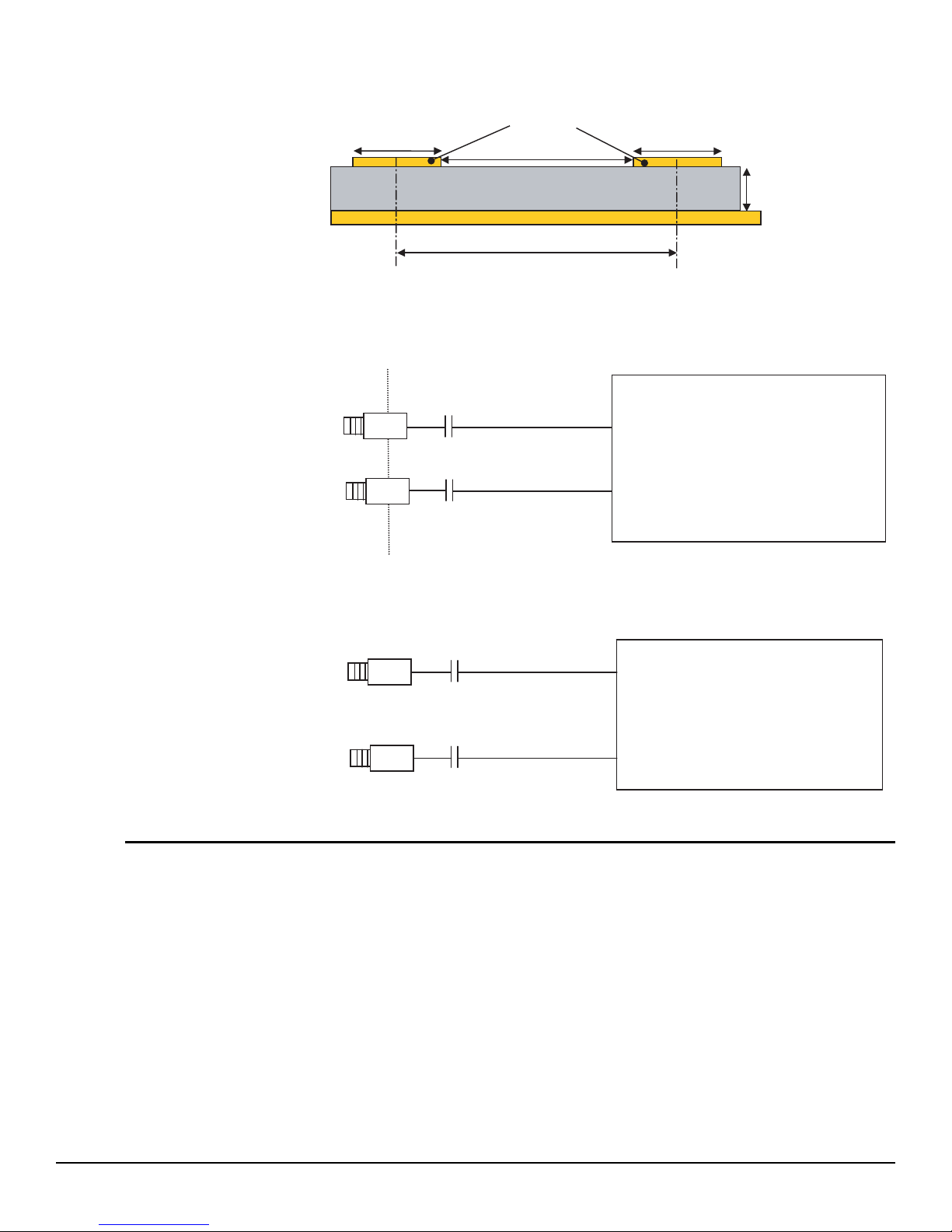
1.2 Description The ADC EV10AS150A Evaluation board is very straightforward as it only implements
the EV10AS150A ADC/DMUX device, SMA connectors for the sampling clock, analog
inputs and reset inputs accesses and HE14 double row 2.54 mm pitch connectors com-
patible with high speed acquisition system probes.
To achieve optimal performance, the ADC EV10AS150A-EB Evaluation board was
designed in a 8-metal-layer board with RO4003 200 µm and FR4 HTG epoxy dielectric
materials. The board implements the following devices:
The ADC EV10AS150A with 1:2/4 DMUX Evaluation board with one version of the
EV10AS150A ADC soldered on the board
Six SMA caps for CLK, CLKN, VIN, VINN, DRR and ASYNCRST signals
Six jumpers DMUX function settings (RS, BIST, DRTYPE, SLEEP, STAGG),
CLKTYPE jumper is not used
3-wire serial link to control ADC functionality via RS232
2.54 mm pitch connectors for the digital outputs, compatible with high speed
acquisition system probes
Banana jacks for the power supply accesses and the die junction temperature
monitoring functions (2 mm)
Potentiometers for the DMUX functions

Introduction
1-2 EV10AS150A-EB User Guide
0977B–BDC–10/09 e2v semiconductors SAS 2009
The board is composed of eight metal layers for signal traces, ground and power supply
layers, and seven dielectric layers featuring low insertion loss and enhanced thermal
characteristics for operation in the high frequency domain.
The board dimensions are 220 mm x 240 mm.
The board comes fully assembled and tested, with one version of the EV10AS150A
ADC installed.
Figure 1-1. ADC EV10AS150A-EB Evaluation Board Simplified Schematic
As shown in Figure 1-1, different power supplies are required:
VCCA5 = 5.0V analog positive power supply
VCCA3 = 3.3V analog positive power supply
VCCD = 3.3V digital positive power supply
VPLUSD = 2.5V digital output power supply
3.3V power supply for the board functions
PIN 1
Port D
Port C
Port B
Port A
DMUX functions
VIN
VINN
CLKNCLK
ASYNCRST
DRR
Diode
CLKDACTRL
G
N
D
3
V
3
G
N
D
G
N
D
G
N
D
DR
ADC
EV10AS150A
G
N
D
V
C
C
A
3
3
V
3
V
C
C
A
5
5
v
2
V
C
C
D
3
v
3
V
+
D
2
V
5
DMUX functions
RS232

EV10AS150A-EB User Guide 2-1
0977B–BDC–10/09
e2v semiconductors SAS 2009
Section 2
Hardware Description
2.1 Board Structure
In order to achieve optimum full speed operation of the ADC EV10AS150A with 1:2/4
DMUX, a multilayer board structure was retained for the evaluation board. Eight copper
layers are used, respectively dedicated to the signal traces, ground planes, power sup-
ply planes and DC signals traces.
The board is made in RO4003 200 µm and FR4 HTG epoxy dielectric materials. Table
2-1 gives a detailed description of the board's structure.
Table 2-1. Board Layer Thickness Profile
Layer Characteristics
Layer 1
Copper layer
Copper thickness = 40 µm
AC signals traces = 50Ωmicrostrip lines
DC signals traces (DMUX functionality etc.)
Layer 2
RO4003 dielectric layer (Hydrocarbon/wovenglass)
Layer thickness = 200 µm
Dielectric constant = 3.4 at 10 GHz
–0.044 dB/inch insertion loss at 2.5 GHz
–0.318 dB/inch insertion loss at 18 GHz
Layer 3
Copper layer
Copper thickness = 35 µm
Upper ground plane = reference plane 50Ωmicrostrip return
Layer 4
FR4 HTG/dielectric layer Layer thickness = 170 µm
Layer 5
Copper layer
Copper thickness = 35 µm
Power planes = VCCA5
Layer 6
FR4 HTG/dielectric layer Layer thickness = 200 µm
Layer 7
Copper layer
Copper thickness = 35 µm
Power planes = VCCD and 3.3V
Layer 8
FR4 HTG/dielectric layer Layer thickness = 170 µm

Hardware Description
2-2 EV10AS150A-EB User Guide
0977B–BDC–10/09 e2v semiconductors SAS 2009
The board is 1.6 mm thick.
The clock, analog input, reset and digital data output signals occupy the top metal layer
while the ADC and DMUX functions are located both on the top.
The ground planes occupy layer 3, 13 and 15 (partly).
Layer 5, 7, 9 and 11 are dedicated to the power supplies.
2.2 Analog
Inputs/Clock
Input
The differential active inputs (Clock, Analog) are provided by SMA connectors.
Reference: VITELEC 142-0701-8511
Special care was taken for the routing of the analog input and clock input signals for
optimum performance in the high frequency domain:
50Ωlines matched to ±0.1 mm (in length) between VIN and VINN and between CLK
and CLKN
50 mm max line length
1.27 mm pitch between the differential traces
400 µm line width
40 µm thickness
850 µm diameter hole in the ground layer below the VIN, VINN, CLK and CLKN ball
footprints
Layer 9
Copper layer
Copper thickness = 35 µm
Power planes = VCCA3
Layer 10
FR4 HTG/dielectric layer Layer thickness = 200 µm
Layer 11
Copper layer
Copper thickness = 35 µm
Power planes = VPLUSD
Layer 12
FR4 HTG/dielectric layer Layer thickness = 170 µm
Layer 13
Copper layer
Copper thickness = 35 µm
Ground plane = reference plane (identical to layer 3)
Layer 14
FR4 HTG/dielectric layer Layer thickness = 200 µm
Layer 15
Copper layer
Copper thickness = 40 µm
DC signals traces and Serial Interface (AVR) signals
Ground plane
Table 2-1. Board Layer Thickness Profile (Continued)

Hardware Description
EV10AS150A-EB User Guide 2-3
0977B–BDC–10/09
e2v semiconductors SAS 2009
Figure 2-1. Figure 2-1.Board Layout for the Differential Analog and Clock Inputs
Figure 2-2. Differential Analog Inputs Implementation
Figure 2-3. Differential Clock Inputs Implementation
2.3 Digital Output The digital output lines were designed with the following recommendations:
50Ωlines matched to ±0.5 mm (in length) between signal of the same differential pair
80 mm max line length
±1 mm line length difference between signals of two ports
±1.5 mm max line length difference between all signals
770 µm pitch between the differential traces
370 µm line width
40 µm thickness
200
µ
m
RO4003
400 µm 400
µm
870
µm
µ1270 m
e= 40µm
Ground plane
VIN (H27)
VINN (J27)
VIN
VINN
100 pF
100 pF
EV10AS150A
100 pF
CLK
CLKN
CLK (W23)
CLKN (RW24)
100 pF
EV10AS150A

Hardware Description
2-4 EV10AS150A-EB User Guide
0977B–BDC–10/09 e2v semiconductors SAS 2009
Figure 2-4. Board Layout for the Differential Digital Outputs
The digital outputs are compatible with LVDS standard. They are on-board 100Ωdiffer-
entially terminated as described in Figure 2-5.
Figure 2-5. Differential digital Outputs Implementation
HE14 Double row 2.54 mm pitch connectors are used for the digital output data. The
upper row is connected to the signal while the lower row is connected to Ground, as
illustrated in Figure 2-6.
Figure 2-6. Differential Digital Outputs 2.54 mm Pitch Connector (Example Port A)
Figure 2-7. Differential Digital Clock Outputs 2.54 Mm Pitch Connector
200 µm
RO4003
3
7
0
µ
m
370µm
400 µm
770 µm
e= 40µm
Ground Plane
Di
DiN
100Ω
50Ω
Line
50Ω
Line
DRN
DR
100Ω
50Ω
Line
50Ω
Line
A0N A0 AORN
/DRA
AOR
/DRAN
…
Ground
Signal
GND A0N A0 A1N AORN AOR GND B0
GND GND GND GND GND GND GND GND
DR DRN
Signal
Ground

Hardware Description
EV10AS150A-EB User Guide 2-5
0977B–BDC–10/09
e2v semiconductors SAS 2009
2.4 Reset Lines
The reset line (DRR and ASYNCRST) were designed with the following recommendations:
50Ωlines
80 mm max line length
430 µm line width
40 µm thickness
Figure 2-8. Board Layout for the Single Reset Lines
200 µm
RO4003
430 µme=40
µ
m

Hardware Description
2-6 EV10AS150A-EB User Guide
0977B–BDC–10/09 e2v semiconductors SAS 2009

EV10AS150A-EB User Guide 3-1
0977B–BDC–10/09
e2v semiconductors SAS 2009
Section 3
Operating Characteristics
3.1 Introduction This section describes a typical configuration for operating the evaluation board of the
ADC EV10AS150A with 1:2/4 DMUX.
The analog input signal can be entered either in differential or single ended. Refer to the
datasheet for the impact of driving analog input in single or in differential. The clock input
signal must be differentially driven.
ADC EV10AS150 clock inputs should be fed with balanced signals (use a balun or
hybrid junction to convert a single signal to a differential signal).
3.2 Operating
Procedure
1. Connect the power supplies and ground accesses through the dedicated banana
jacks.
VCCA5 = 5.0V, VCCA3 = 3.3V, VCCD = 3.3V, VPLUSD = 2.5V,
VCCA3 = 3.3V, VCCD = 3.3V and 3.3V have separated planes but can be reunited via a
short-cable.
2. Connect the clock input signals. Use a low-phase noise high frequency
generator.
The clock input level is typically 1dBm (on 100Ωdifferential input). The clock frequency
can range from 500 MHz up to maximum speed.
3. Connect the analog input signal. Use a low-phase noise high frequency
generator.
The analog input full scale is 500 mV peak-to-peak (±250 mV on each single ended
input) around 0V (AC coupling). It is recommended to use the ADC with an input signal
of –1 dBFS max (to avoid saturation of the ADC).
The analog input frequency can range from DC up to 5 GHz. At 5 GHz, the ADC attenu-
ates the input signal by 3 dB.
4. Connect the high-speed acquisition system probes to the output connectors.
The digital data are differentially terminated on-board (100Ω) however, they can be
probed either in differential or in single-ended mode.
5. Connect the DMUX function jumpers:
All instrumentation and connectors are now connected.
6. Switch on the power supplies (No specific power supplies sequencing required
during power on/off).
7. Turn on the RF clock generator.
8. Turn on the RF signal generator.

Operating Characteristics
3-2 EV10AS150A-EB User Guide
0977B–BDC–10/09 e2v semiconductors SAS 2009
9. Perform an asynchronous Reset (DRR active) on the device and maintain this
Reset active.
10. Perform an asynchronous Reset ((push button) ASYNCRST active) on the
board.
11. Then, ASYNCRST inactive on the board.
12. DRR inactive on the device.
13. Started 3 Wire Serial interface (refer to Section 4)
14. Reset button allows to configure ADC (Mode 0)
3.3 Electrical
Characteristics
Table 3-1. Absolute Maximum Ratings
Parameter Symbol Value Unit
Analog 5.0V Power Supply voltage VCCA5 GND to 6.0 V
Analog 3.3V Power Supply voltage VCCA3 GND to 3.6 V
Digital 3.3V Power Supply Voltage VCCD GND to 3.6 V
Output 2.5V Power Supply voltage VPLUSD GND to 3.0 V
Minimum Analog input peak voltage
(with differential input)
VIN or VINN 2.0 V
Maximum Analog input peak voltage
(with differential input)
VIN or VINN 4.0 V
Maximum difference between VIN and
VINN
(with differential input)
|VIN - VINN|2.0
(4 Vpp = +13 dBm in 100 Ω)
V
Minimum Analog input peak voltage
(with single ended input)
VIN with VINN = 50Ωto GND
or
VINN with VIN = 50Ωto GND
2.0 V
Maximum Analog input peak voltage
(with single ended input)
VIN with VINN = 50Ωto GND
or
VINN with VIN = 5 Ωto GND
4.0 V
Maximum amplitude on VIN or VINN
(with single ended input)
|VIN|or |VINN| (2 Vpp = +10 dBm in 50Ω)V
Minimum Clock input peak voltage
(with differential clock)
VCLK or VCLKN 1.5 V
Maximum Clock input peak voltage
(with differential clock)
VCLK or VCLKN 4.0 V
Maximum difference between VCLK
and VCLKN
(with differential clock)
|VCLK -VCLKN|1.5
(3 Vpp)
V
3WSI input voltage SDATA, SLDN, SCLK, RESET –0.3 to VCCA3 + 0.3 V
ADC Reset Voltage DRR –0.3 to VCCA3 + 0.3 V
DMUX function input voltage RS, DRTYPE, SLEEP, STAGG, BIST –0.3 to VCCD + 0.3 V
DMUX Asynchronous Reset ASYNCRST –0.3 to VCCD + 0.3 V

Operating Characteristics
EV10AS150A-EB User Guide 3-3
0977B–BDC–10/09
e2v semiconductors SAS 2009
Note: Absolute maximum ratings are limiting values (referenced to GND = 0V), to be applied individually, while other parameters are
within specified operating conditions. Long exposure to maximum rating may affect device reliability.
All integrated circuits should be handled with appropriate care to avoid damages due to ESD. Damage caused by inappropriate
handling or storage could range from performance degradation to complete failure, including reliability degradation.
DMUX Control Voltage CLKDACTRL –0.3 to VCCD + 0.3 V
Maximum input voltage on DIODE DIODE ADC 700 mV
Maximum input current on DIODE DIODE ADC 1 mA
Max Junction Temperature TJ135 °C
Storage temperature Tstg –55 to 150 °C
ESD protection (HBM) ≥500 on ADC inputs
500 on DMUX outputs
V
Table 3-1. Absolute Maximum Ratings (Continued)
Table 3-2. Electrical Characteristics for Supplies
Parameter
Test
Level Symbol Min Typ Max Unit
POWER REQUIREMENTS
Power Supply voltages
Analog 5.0V
Analog 3.3V
Digital 3.3V
Output 2.5V
1
VCCA5
VCCA3
VCCD
VPLUSD
4.85
3.15
3.15
2.4
5.0
3.3
3.3
2.5
5.15
3.45
3.45
2.6
V
V
V
V
Power Supply current in 1:2 DMUX
Analog VCCA5 = 5.0V
Analog VCCA3 = 3.3V
Digital VCCD = 3.3V
Output VPLUSD = 2.5V
1
IVCCA5
IVCCA3
IVCCD
IVPLUSD
160
775
400
420
200
960
500
610
mA
mA
mA
mA
Power Supply current in 1:4 DMUX
Analog VCCA5 = 5.0V
Analog VCCA3 = 3.3V
Digital VCCD = 3.3V
Output VPLUSD = 2.5V
1
IVCCA5
IVCCA3
IVCCD
IVPLUSD
160
775
450
450
200
960
580
650
mA
mA
mA
mA
Power Supply current in NAP and SLEEP mode
Analog VCCA5 = 5.0V
Analog VCCA3 = 3.3V
Digital VCCD = 3.3V
Output VPLUSD = 2.5V
1
IVCCA5
IVCCA3
IVCCD
IVPLUSD
140
590
140
410
190
870
180
560
mA
mA
mA
mA
Power dissipation
- 1:2 DMUX
- 1:4 DMUX
- NAP & SLEEP mode (1:4 or 1:2)
1 PD
6.2
6.4
4.4
7.6
8.0
6.0
W
W
W

Operating Characteristics
3-4 EV10AS150A-EB User Guide
0977B–BDC–10/09 e2v semiconductors SAS 2009
3.4 Digital Output
Coding
MSB bit 9 and LSB bit 0.
Note: 1. Refer to chap. 4.4.4 and 4.4.5 for selection between natural binary, binary 2's complement or Gray coding.
Table 3-3. Digital Output Coding
Differential
Analog Input Voltage Level Digital Output
Natural Binary(1)
MSB……….LSB OR
Binary 2’s Complement(1)
MSB……....LSB OR
Gray Coding(1)
MSB……..LSB OR
> 250.25 mV >Top end of full scale + ½ LSB 1 1 1 1 1 1 1 1 1 1 1 0 1 1 1 1 1 1 1 1 1 1 1 0 0 0 0 0 0 0 0 0 1
250.25 mV
249.75 mV
Top end of full scale + ½ LSB
Top end of full scale - ½ LSB
1 1 1 1 1 1 1 1 1 1 0
1 1 1 1 1 1 1 1 1 0 0
0 1 1 1 1 1 1 1 1 1 0
0 1 1 1 1 1 1 1 1 0 0
1 0 0 0 0 0 0 0 0 0 0
1 0 0 0 0 0 0 0 0 1 0
125.25 mV
124.75 mV
3/4 full scale + ½ LSB
3/4 full scale - ½ LSB
1 1 0 0 0 0 0 0 0 0 0
1 0 1 1 1 1 1 1 1 1 0
0 1 0 0 0 0 0 0 0 0 0
0 0 1 1 1 1 1 1 1 1 0
1 0 1 0 0 0 0 0 0 0 0
1 1 1 0 0 0 0 0 0 0 0
0.25 mV
–0.25 mV
Mid scale + ½ LSB
Mid scale - ½ LSB
1 0 0 0 0 0 0 0 0 0 0
0 1 1 1 1 1 1 1 1 1 0
0 0 0 0 0 0 0 0 0 0 0
1 1 1 1 1 1 1 1 1 1 0
1 1 0 0 0 0 0 0 0 0 0
0 1 0 0 0 0 0 0 0 0 0
–124.75 mV
–124.25 mV
1/4 full scale + ½ LSB
1/4 full scale - ½ LSB
0 1 0 0 0 0 0 0 0 0 0
0 0 1 1 1 1 1 1 1 1 0
1 1 0 0 0 0 0 0 0 0 0
1 0 1 1 1 1 1 1 1 1 0
0 1 1 0 0 0 0 0 0 0 0
0 0 1 0 0 0 0 0 0 0 0
–249.75 mV
–250.25 mV
Bottom end of full scale + ½ LSB
Bottom end of full scale - ½ LSB
0 0 0 0 0 0 0 0 0 1 0
0 0 0 0 0 0 0 0 0 0 0
1 0 0 0 0 0 0 0 0 1 0
1 0 0 0 0 0 0 0 0 0 0
0 0 0 0 0 0 0 0 0 1 0
0 0 0 0 0 0 0 0 0 0 0
<–250.25 mV < Bottom end of full scale - ½ LSB 0 0 0 0 0 0 0 0 0 0 1 1 0 0 0 0 0 0 0 0 0 1 0 0 0 0 0 0 0 0 0 0 1

EV10AS150A-EB User Guide 4-1
0977B–BDC–10/09
e2v semiconductors SAS 2009
Section 4
Software Tools
4.1 Overview The ADC EV10AS150A evaluation user interface software is a C++ compiled graphical
interface.
No license is required to run on a W98, NT, W2000 and XP PC.
The software uses intuitive push buttons and popup menus to write data from the
hardware.
4.2 Configuration Advised configuration for Win2000:
– PC Pentium >100 MHz
– Memory 24Mo
– For other versions of Windows OS, use the recommended configuration from
Microsoft
– Two COM ports are necessary to use two boards simultaneously
4.3 Getting Started Install the ADC EV10AS15x application on your computer by launching the EV10AS15x
exe installer.

Software Tools
4-2 EV10AS150A-EB User Guide
0977B–BDC–10/09 e2v semiconductors SAS 2009
Figure 4-1. Install Window
Start the Setup_EV10AS15x (v1.1.2)
Figure 4-2. EV10AS150A Application Set up Wizard Window

Software Tools
EV10AS150A-EB User Guide 4-3
0977B–BDC–10/09
e2v semiconductors SAS 2009
Next step: Select Destination Directory.
Figure 4-3. EV10AS150A select Destination Directory Window
Next step: Start Menu Folder.
Figure 4-4. EV10AS150A select Start Menu Window

Software Tools
4-4 EV10AS150A-EB User Guide
0977B–BDC–10/09 e2v semiconductors SAS 2009
Next step: verification of the install configuration.
Figure 4-5. EV10AS150A Ready to Install Window
If you agree with the install configuration press Install.
Figure 4-6. EV10AS150A Application Setup Install Push Button
The software is completing installation.
Figure 4-7. EV10AS150A Completing Setup Wizard Window
Table of contents
Other e2v Motherboard manuals