e2v AT84CS001-EB User manual

AT84CS001-EB Evaluation Board
..............................................................................................
User Guide


AT84CS001-EB Evaluation Board User Guide i
0904C–BDC–09/07
Table of Contents
Section 1
Introduction ............................................................................................. 1
1.1 Scope ..............................................................................................................1
1.2 Description ......................................................................................................1
Section 2
Hardware Description ............................................................................. 1
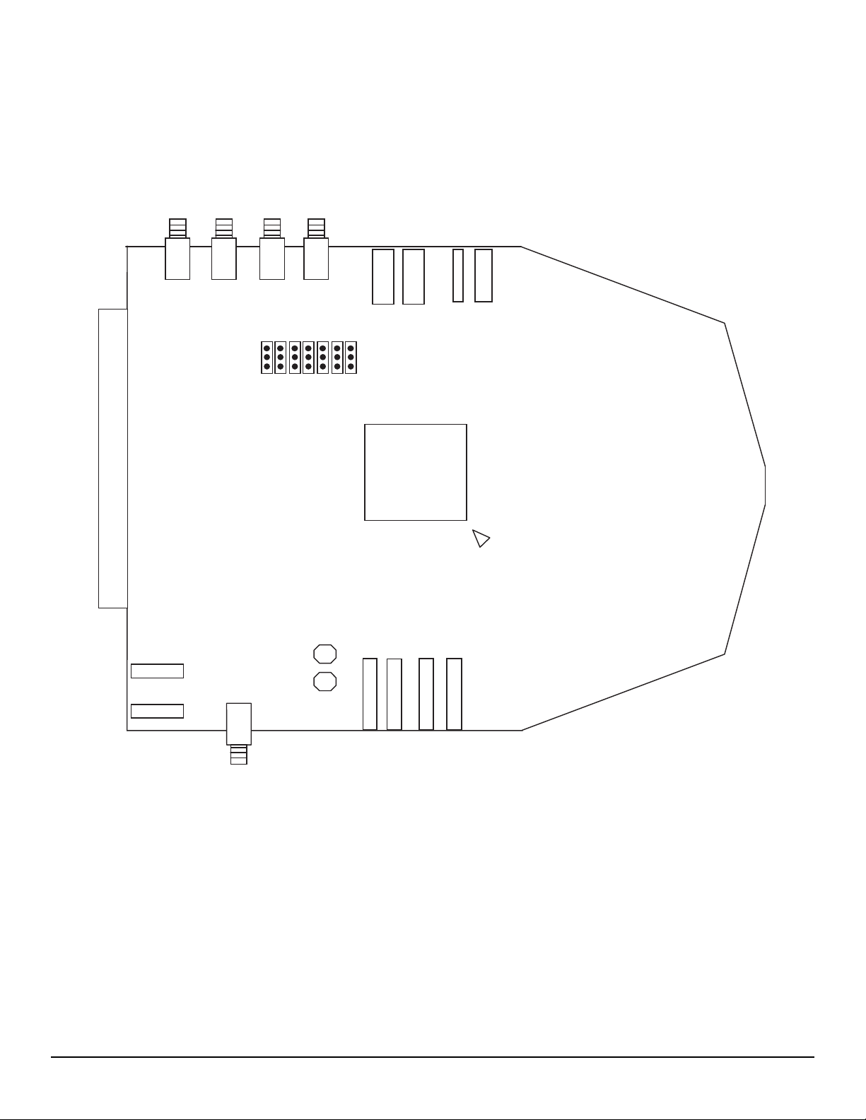
2.1 Board Structure 1
2.2 Data and Clock Input Accesses ......................................................................2
2.3 Digital Output 2
2.4 ASYNCRST .................................................................................................... 3
2.5 Standalone Delay Cell .................................................................................... 3
2.6 DMUX Functions............................................................................................. 3
2.7 Power Supplies ...............................................................................................3
Section 3
Operating Characteristics ....................................................................... 1
3.1 Introduction .....................................................................................................1
3.2 Operating Procedure ......................................................................................1
3.3 Electrical Characteristics ................................................................................2
Section 4
Application Information ........................................................................... 1
4.1 Introduction ..................................................................................................... 1
4.2 Input Data .......................................................................................................1
4.3 Digital Outputs ................................................................................................ 1
4.4 DMUX Functions .............................................................................................2
4.4.1 ASYNCRST ..............................................................................................2
4.4.2 CLKDACTRL ............................................................................................2
4.4.3 DACTRL ...................................................................................................3
4.4.4 RS, DRTYPE, DAEN, BIST, CLKTYPE, SLEEP, STAGG .......................4
4.5 Test bench Description ...................................................................................6
Section 5
Package Information ............................................................................... 1
5.1 AT84CS001 Pinout .........................................................................................1
5.2 Package Outline .............................................................................................5
Section 6

ii AT84CS001-EB Evaluation Board User Guide
0904C–BDC–09/07
Ordering Information ............................................................................... 1
Section 7
Appendix ................................................................................................. 1
7.1 AT84CS001-EB Electrical Schematics ...........................................................1
7.2 AT84CS001-EB Board Layers ........................................................................5

AT84CS001-EB Evaluation Kit User Guide 1-1
0904C–BDC–09/07
Section 1
Introduction
1.1 Scope
The AT84CS001-EB Evaluation Kit is designed to facilitate the evaluation and charac-
terization of the AT84CS001 1:2/4 10-bit 2.2 GHz DMUX up to 2.2 GHz.
The AT84CS001-EB Evaluation Kit includes
The 1:2/4 10-bit 2.2 GHz DMUX Evaluation Board
Five SMA caps for DAI, DAIN, DAO, DAON and ASYNCRST signals
Seven jumpers for the DMUX function settings (RS, BIST, CLKTYPE, DRTYPE,
SLEEP, STAGG, DAEN)
This user guide uses the AT84CS001-EB evaluation Kit as an evaluation and demon-
stration platform and provides guidelines for its correct use.
1.2 Description
The AT84CS001-EB evaluation board is very straightforward as it only implements the
AT84CS001 1:2/4 10-bit 2.2 GHz DMUX device, SMA connectors for the standalone
delay cell inputs and outputs and for the reset input accesses and 2.54 mm pitch con-
nectors compatible with high-speed acquisition system probes.
This evaluation board is fully compatible with e2v high-speed ADC boards
(TSEV830500GL, TSEV8388BGL/GLZA2/F/FZA2, TSEV83102G0BGL and
AT84AS008GL-EB).
To achieve optimal performance, the AT84CS001-EB evaluation board was designed in
a 4-metal-layer board with RO4003 200 and FR4 HTG dielectric layers. The board
implements the following devices:
The 1:2/4 10-bit 2.2 GHz DMUX Evaluation board
Five SMA caps for DAI, DAIN, DAO, DAON and ASYNCRST signals
Seven jumpers for the DMUX function settings (RS, BIST, CLKTYPE, DRTYPE,
SLEEP, STAGG, DAEN)
2.54 mm pitch connectors for the digital inputs and outputs, compatible with high-
speed acquisition system probes
Banana jacks for the power supply accesses
Potentiometers for the DMUX control functions

Introduction
1-2 AT84CS001-EB Evaluation Kit User Guide
0904C–BDC–09/07
The board is comprised of four metal layers for signal traces, ground and power supply
layers, and three dielectric layers featuring low insertion loss and enhanced thermal
characteristics for operation in the high frequency domain.
The board dimensions are 220 mm x 230 mm.
The board comes fully assembled and tested, with the AT84CS001 installed.
Figure 1-1. Simplified Schematics of the AT84CS001-EB Evaluation Board
As shown in Figure 1-1, different power supplies are required:
V
CCD
= 3.3V digital positive power supply
V
PLUSD
= 2.5V digital output power supply
3.3V used for the DMUX functions
PIN 1
Port D
Port C
Port B
Port A
DMUX functions
ASYNCRST
3.3V GND
DAO/DAON
G
N
D
DR
DAI/DAIN
AT84CS001
V-GND
I-GND
Data and Clock
Inputs
CLKDACTRL
DACTRL
V
+
D
V
C
C
D
VCCD
3.3V
G
N
D

AT84CS001-EB Evaluation Kit User Guide 2-1
0904C–BDC–09/07
Section 2
Hardware Description
2.1 Board Structure
In order to achieve optimum full-speed operation of the AT84CS001 1:2/4 10-bit 2.2
GHz DMUX, a multi-layer board structure was retained for the evaluation board. Four
copper layers are used, respectively dedicated to the signal traces, ground planes and
power supply planes.
The board is made in RO4003 200 µm and FR4 HTG epoxy dielectric materials.
The following table gives a detailed description of the board's structure.
Table 2-1. Board Structure
Layer Characteristics
Layer 1
Copper layer
Copper thickness = 40 µm
Input and output signals traces = 50Ω
microstrip lines
Layer 2
RO4003 dielectric layer
(Hydrocarbon/wovenglass)
Layer thickness = 200 µm
Dielectric constant = 3.4 at 10 GHz
- 0.044 dB/inch insertion loss at 2.5 GHz
- 0.318 dB/inch insertion loss at 18 GHz
Layer 3
Copper layer
Copper thickness = 35 µm
Upper ground plane = reference plane
Layer 4
FR4 HTG/dielectric layer Layer thickness = 1050 µm
Layer 5
Copper layer
Copper thickness = 35 µm
Power planes = 3.3V, V
CCD
and V
PLUSD
Layer 6
FR4 HTG/dielectric layer Layer thickness = 200 µm
Layer 7
Copper layer
Copper thickness = 40 µm
Lower ground plane = reference plane

Hardware Description
2-2 AT84CS001-EB Evaluation Kit User Guide
0904C–BDC–09/07
The board is 1.6 mm thick.
The digital data input, output and reset signals are located on the top metal layer.
The function signals are located on the top metal layer and layer 7.
The ground planes are located on layer 3 and 7.
Layer 5 is dedicated to the power supplies (3.3V, V
CCD
and V
PLUSD
).
2.2 Data and Clock
Input Accesses
Access to the digital data and clock inputs is provided by one female 2.54 mm pitch con-
nector (points) via 50Ωmicrostrip lines.
The connector is made of two rows:
The upper row is dedicated to the data and clock signals
The lower row is connected to ground
Each differential signal pair is separated by a connection to ground, as illustrated in
Figure 2-1
Figure 2-1. Input Data Connector
The input lines are matched (in length) within ±1 mm.
Note: 100Ωtermination is provided on-chip.
2.3 Digital Output
Access to the digital data and clock outputs is provided by four male 2.54 mm pitch con-
nectors (points) via 50Ωmicrostrip lines.
The connector is made of two rows:
The upper row is dedicated to the data and clock signals
The lower row is connected to ground
Each output port is separated by a connection to ground, as illustrated in Figure 2-2 on
page 2-3.
GND I9 I9N GND GND I0 I0N GND
GND GND GND GND GND GND GND GND
IOR IORN GND
GND GND GND

Hardware Description
AT84CS001-EB Evaluation Kit User Guide 2-3
0904C–BDC–09/07
Figure 2-2. Output Data Connector
The digital outputs are compatible with LVDS standard. They are on-board 100Ωdiffer-
entially terminated as described in Figure 2-3.
Figure 2-3. Differential Digital Outputs Implementation
The output lines are matched (in length) within ± 5 mm.
2.4 ASYNCRST
Access to the asynchronous reset is provided by both an SMA connector and a push
button.
2.5 Standalone
Delay Cell
Access to the standalone delay cell inputs (DAI/DAIN) and outputs (DAO/DAON) is pro-
vided by SMA connectors via 50Ωmicrostrip lines.
Note: The 100Ωtermination for the DAI/DAIN inputs is provided on-chip, the
DAO/DAON outputs are floating (must be terminated by 100Ωtermination).
2.6 DMUX Functions
Two potentiometers are provided for the DMUX input clock delay control (CLKDACTRL)
and the standalone delay cell control (DACTRL).
Seven jumpers are provided for the RS, BIST, DAEN, SLEEP, STAGG, CLKTYPE and
DRTYPE functions (jumper on board = logic 0).
2.7 Power Supplies
Layer 5 is dedicated to power supply planes (3.3V, V
CCD
and V
PLUSD
).
The supply traces are low impedance and are surrounded by two ground planes (layers
3 and 7).
V
CCD
and 3.3V have separated planes but can be short-circuited on the board. The 3.3V
supply was separated from V
CCD
for device power consumption testing purposes.
Each incoming power supply is bypassed at the banana jack by a 1 µF Tantalum capac-
itor in parallel with a 100 nF chip capacitor.
GND A0N A0 A1N
AORN/
DRA
AOR/
DRAN
GND B0
GND GND GND GND GND GND GND GND
Data
DataN
100Ω
50Ωline
50Ωline

Hardware Description
2-4 AT84CS001-EB Evaluation Kit User Guide
0904C–BDC–09/07
Each power supply is decoupled as close as possible to the AT84CS001 device by
10 nF in parallel with 100 pF surface mount chip capacitors.
Note: The decoupling capacitors are superimposed with the 100 pF capacitor
mounted first.

AT84CS001-EB Evaluation Kit User Guide 3-1
0904C–BDC–09/07
Section 3
Operating Characteristics
3.1 Introduction
This section describes a typical configuration for operating the evaluation board of the
AT84CS001 1:2/4 10-bit 2.2 GHz DMUX.
3.2 Operating
Procedure
The procedure described below helps you operate the evaluation board for the first time.
It described the steps to accomplish a BIST in order to verify whether the board is func-
tional or not. At the end of the procedure, the DMUX is in the following configuration:
BIST, 1:4 ratio, CLKTYPE = CLK/2, DRTYPE = DR/2, simultaneous mode, no SLEEP.
Note: Do not switch the power supplies until all power connections on the evaluation
board are established.
1. Connect the power supplies and ground accesses through the dedicated banana
jacks. V
CCD
= 3.3V, V
PLUSD
= 2.5V and 3.3V.
2. Connect the clock input signals (CLK, CLKN). This clock may be single-ended or
differential. Use a low-phase noise high frequency generator. You should use an
LVDS signal to drive the input clock.
In single-ended mode, CLK must have a common mode voltage equal to 1.25V
and CLKN should be connected to a constant value equal to 1.25V. For a differ-
ential signal use an LVDS buffer. The clock frequency can range from 1 MHz up
to 1.1 GHz (CLK/2 mode) or 2.2 GHz (CLK mode).
3. Remove the jumpers on CLKTYPE, DRTYPE, RS, DAEN, SLEEP and STAGG.
The only remaining jumper is on BIST.
4. Connect the high-speed acquisition system probes to the output connectors.
The digital data are differentially terminated on-board (100Ω) but, they can be probed
either in differential or in single-ended mode.
All instrumentation and connectors are now connected.
5. Switch on the power supplies (recommended power up sequence: simultaneous
or in the following order: V
CCD
= 3.3V, V
PLUSD
= 2.5V and 3.3V).

Operating Characteristics
3-2 AT84CS001-EB Evaluation Kit User Guide
0904C–BDC–09/07
6. Turn on the RF clock generator
7. Perform an asynchronous reset (ASYNCRST push button) on the device.
The AT84CS001-EB evaluation board is now ready for operation in BIST mode.
Note: The BIST comprises a 10-bit sequence available on all four ports of the device
(sets the AT84CS001 in 1:4 mode).
The sequence is as follows:
Cycle 0: Cycle 1:
Port A = 1010101010 Port A = 0101010101
Port B = 1010101010 Port B = 0101010101
Port C = 0101010101 Port C = 1010101010
Port D = 1010101010 Port D = 0101010101
3.3 Electrical
Characteristics
Note: Absolute maximum ratings are limiting values (referenced to GND = 0V), to be applied individually, while other parameters are
within specified operating conditions. Long exposure to maximum rating may affect device reliability.
All integrated circuits have to be handled with appropriate care to avoid damages due to ESD. Damage caused by inappropriate
handling or storage could range from performance degradation to complete failure.
Table 3-1. Absolute Maximum Ratings
Parameter Symbol Value Unit
Digital power supply V
CCD
3.6 V
Output power supply V
PLUSD
3.6 V
Data input
I0, I0N…I9, I9N
IOR,IORN
DAI, DAIN
-0.3 to V
CCD
+ 0.3 V
Clock input VCLK,VCLKN -0.3 to V
CCD
+ 0.3 V
Control inputs
SLEEP, STAGG, ASYNCRST,
BIST, RS, DAEN, CLKTYPE,
DRTYPE, CLKDACTRL,
DACTRL
-0.3 to V
CCD
+ 0.3 V
Maximum junction temperature TJ 125 °C
Storage temperature Tstg -65 to 150 °C
Ball temperature Tballs 300 °C

Operating Characteristics
AT84CS001-EB Evaluation Kit User Guide 3-3
0904C–BDC–09/07
Table 3-2. Recommended Conditions of Use
Parameter Symbol Comments Recommended Unit
Positive supply voltage V
CCD
3.3 V
Positive digital supply voltage V
PLUSD
2.5 V
DMUX Control Voltage CLKDACTRL,
DACTRL V
CCD
/3 to 2 × V
CCD
/3 V
Operating Temperature Range Industrial “V” grade -40°C < T
C
; T
J
< 110°C °C
Table 3-3. Electrical Operating Characteristics
Parameter Symbol Min Typ Max Unit
Resolution 10-bit with additional 11th bit Bit
Power Requirements
Digital power supply voltage V
CCD
3.15 3.3 3.45 V
Output power supply voltage V
PLUSD
2.375 2.5 2.625 V
Digital power supply current
- 1:2 mode
- 1:4 mode
- SLEEP mode
- Additional current with SDA enabled
- Additional current with BIST enabled
I
VCCD
520
580
170
25
40
610
(3)
680
(3)
200
(3)
mA
Output power supply current
- 1:2 mode
- 1:4 mode
I
VPLUSD
250
280
350
(3)
380
(3)
mA
Power dissipation
- 1:2 mode
- 1:4 mode
- SLEEP mode (1:4)
- All active (1:4, BIST & SDA enabled)
P
D
2.4
2.6
1.3
2.8
3.0
(3)
3.3
(3)
3.5
(3)
W
LVDS Data/Clock Inputs and Outputs
Logic Compatibility LVD S
Input Common Mode
(1)
V
ICM
11.25 1.6 V
Output Common Mode
(2)
V
OCM
1.125 1.25 1.375 V
Differential input
(1)
V
IDIFF
100 350 -mV
Differential output V
ODIFF
250 350 500 mV
Output level "High" V
OH
1.25 1.425 - V
Output level "Low" V
OL
-1.075 1.25 V

Operating Characteristics
3-4 AT84CS001-EB Evaluation Kit User Guide
0904C–BDC–09/07
Notes: 1. Given for a differential input
2. Given for a 100Ωtermination across true/false signals
3. Worst case value obtained with maximum supply voltages over full temperature range
Static Inputs (SLEEP, STAGG, BIST, RS, DAEN, CLKTYPE, DRTYPE)
Control Input Voltages :
- Logic low
- Logic high
R
IL
V
IL
R
IH
V
IL
0
10k
2.0V
10
0.5V
Infinite
Ω
Static Inputs (CLKDACTRL, DACTRL)
Control input voltages V
CCD
/3 2 × V
CCD
/3 V
Reset input (ASYNCRST)
Logic compatibility LVCM OS/ CM O S
Control input voltages:
- Logic low
- Logic high
- Common mode
V
IL
V
IH
V
ICM
0
1.5
1.4
1.2
3.3
V
Table 3-3. Electrical Operating Characteristics (Continued)
Parameter Symbol Min Typ Max Unit
Table 3-4. Switching Performance and Characteristics
Parameter Symbol Min Typ Max Unit
Input Clock
Maximum clock frequency Fs max 11500 MHz
Minimum clock pulse width (high) TC1 0.3 0.333 500 ns
Minimum clock pulse width (low) TC2 0.3 0.333 500 ns
Output rise/fall time for data (20% -
80%) TR/TF 400 ps
Output rise/fall time for Data Ready
(20% - 80%) TR/TF 400 ps
Data output delay TOD 400 ps
Data Ready output delay TDR 400 ps
|TOD - TDR| 0ps

Operating Characteristics
AT84CS001-EB Evaluation Kit User Guide 3-5
0904C–BDC–09/07
Note: Please refer to the device datasheet entitled “ AT84CS001”, reference 0809.
Output data to Data Ready
propagation delay TD1 0.3 0.333 500 ps
Data Ready to output data
propagation delay TD2 0.3 0.333 500 ps
Output data pipeline delay:
- Synchronized 1:2 mode
- Synchronized 1:4 mode
- Staggered 1:2 mode
- Staggered 1:4 mode
TPD
0.5
1.5
0 / 0.5
0 / 0.5 / 1 / 1.5
Clock cycles
Table 3-4. Switching Performance and Characteristics (Continued)
Parameter Symbol Min Typ Max Unit

Operating Characteristics
3-6 AT84CS001-EB Evaluation Kit User Guide
0904C–BDC–09/07

AT84CS001-EB Evaluation Kit User Guide 4-1
0904C–BDC–09/07
Section 4
Application Information
4.1 Introduction
For this section, please also refer to the "Main features" section in the ”AT84CS001”
reference 0809.
4.2 Input Data
The input data (I0, I0N…I9, I9N and IOR, IORN) and clock (CLK, CLKN) as well as the
DAI, DAIN input data of the standalone delay cell are LVDS compatible (on-chip 100Ω).
Figure 4-1. Input Data and Clock Signals
4.3 Digital Outputs
The digital outputs (data and Data Ready) are LVDS compatible. The 100Ωdifferential
termination is provided on-board.
50Ωline
Data or clock
inverted phase signal
Data or clock in
phase signal
50Ωline

Application Information
4-2 AT84CS001-EB Evaluation Kit User Guide
0904C–BDC–09/07
Figure 4-2. Implementation of Differential Digital Outputs
4.4 DMUX Functions
4.4.1 ASYNCRST The asynchronous reset is mandatory to start the device properly. It must be applied
after power up of the device and after any change of DMUX function.
A push button is provided to perform this reset and pull-up and pull-down resistors main-
tain the ASYNCRST signal in inactive mode.
Figure 4-3. ASYNCRST Function
If the DRRB reset is also used, we recommend to apply the asynchronous reset while
the DRRB reset is active.
The first data is available at the device output after TOD + 7.5 cycles.
4.4.2 CLKDACTRL A delay cell is provided to allow you to tune the delay between the clock and data at the
DMUX input. The delay is controlled via the CLKDACTRL potentiometer.
This cell allows you to delay the internal DMUX clock by approximately 250 ps via the
CLKDACTRL potentiometer (varying from V
CCD
/3 to (2 × V
CCD
)/3).
Di
DiN
100Ω
50Ω line
DRN
DR
100Ω
50Ωline
50Ωline
50Ωline
3.3V
GND
AT84CS001
3.3V
15 KΩ
4.7 KΩ

Application Information
AT84CS001-EB Evaluation Kit User Guide 4-3
0904C–BDC–09/07
Figure 4-4. CLKDACTRL Function
4.4.3 DACTRL A standalone delay cell is available (input = DAI/DAIN, output = DAO/DAON, control =
DACTRL, enable = DAEN). This cell allows you to delay the incoming signal DAI/DAIN
by approximately 250 ps via the DACTRL potentiometer (varying from V
CCD
/3 to (2 ×
(V
CCD
)/3).
3.3V
10 KΩ
10 KΩ
10 KΩ
GND
AT84CS001

Application Information
4-4 AT84CS001-EB Evaluation Kit User Guide
0904C–BDC–09/07
4.4.4 RS, DRTYPE, DAEN,
BIST, CLKTYPE,
SLEEP, STAGG
Seven jumpers are provided for the RS, DRTYPE, DAEN, BIST, CLKTYPE, SLEEP and
STAGG functions. The following table describes each of these functions.
Note: The BIST is comprised of a 10-bit sequence available on all four ports of the device (sets the AT84CS001 in 1:4 mode). The
sequence is as follows:
Cycle 0:
Port A = 1010101010
Port B = 1010101010
Port C = 0101010101
Port D = 1010101010
Cycle 1:
Port A = 0101010101
Port B = 0101010101
Port C = 1010101010
Port D = 0101010101
Table 4-1. Settings and Description of each DMUX Function
Function Description Jumper Settings
BIST
Built-In Self Test:
- Active: checker-board pattern available at the
device’s output
- Inactive: normal mode
BIST: jumper ON
No BIST: jumper OUT
CLKTYPE
Input clock mode:
- CLK= data valid on each rising edge of the
CLK/CLKN signal
- CLK/2 = data valid on both rising and falling edges of
the CLK/CLKN signal
CLK: jumper ON
CLK/2: jumper OUT
DAEN
Standalone Delay Cell Enable
- DAEN active: DAI/DAIN delay can be controlled via
DACTRL and output in DAO/DAON
- DAEN inactive: the standalone delay cell cannot be
used
DAEN active : jumper ON
DAEN inactive: jumper OUT
DRTYPE
Output clock mode:
- DR/2 = data valid on both rising and falling edges of
the DR/DRN signal
- DR = data valid on each rising edge of the DR/DRN
signal
DR/2: jumper ON
DR: jumper OUT
RS
Ratio selection:
- 1:2
- 1:4
Jumper ON
Jumper OUT
SLEEP
Sleep mode:
- Active: the device is in a partial standby mode
- Inactive: normal mode
SLEEP: jumper ON
Inactive: jumper OUT
STAGG
Simultaneous or staggered output mode:
- STAGG acitve: staggered output data
- Inactive: simultaneous output data
STAGG: jumper ON
Inactive: jumper OUT
Table of contents
Other e2v Motherboard manuals