e2v EV8AQ160-EB User manual

EV8AQ160-EB Evaluation Board
..............................................................................................
User Guide


EV8AQ160-EB - User Guide i
0834E–BDC–07/09
e2v semiconductors SAS 2009
Table of Contents
Section 1
1.1 Scope........................................................................................................1-3
1.2 Description ................................................................................................1-3
Section 2
2.1 Board Structure.........................................................................................2-5
2.2 Analog Inputs/Clock Input .........................................................................2-6
2.3 Digital Output ............................................................................................2-6
2.4 Reset Inputs..............................................................................................2-7
2.5 Power Supplies .........................................................................................2-9
Section 3
3.1 Introduction .............................................................................................3-11
3.2 Operating Procedure...............................................................................3-11
3.3 Electrical Characteristics.........................................................................3-12
Section 4
4.1 Overview .................................................................................................4-15
4.2 Configuration...........................................................................................4-15
4.3 Getting Started........................................................................................4-15
4.4 Troubleshooting ......................................................................................4-22
4.5 Installation Software................................................................................4-23
4.6 Operating Modes ....................................................................................4-24
4.6.1 Settings.............................................................................................4-25
4.6.2 Test...................................................................................................4-29
4.6.3 Gain/Offset/Phase ............................................................................4-30
4.7 INL ..........................................................................................................4-33
4.7.1 INL Calibration Procedure ................................................................4-34
4.8 Input Impedance .....................................................................................4-39
Section 5
5.1 Analog Input............................................................................................5-43
5.2 ..............................................................................................Clock Input5-44
5.3 RESET input ...........................................................................................5-44
5.4 Output Data.............................................................................................5-45
5.5 CMIRefAB and CMIRefCD Output Signals .............................................5-45
5.6 Diode for Junction Temperature Monitoring............................................5-45
5.7 Test Bench Description...........................................................................5-46
Section 6

ii EV8AQ160-EB - User Guide
0834E–BDC–07/09
e2v semiconductors SAS 2008
6.1 Ordering Information ...............................................................................6-47
Section 7
7.1 EV8AQ160-EB Electrical Schematics .....................................................7-49
7.2 EV8AQ160-EB Board Layers..................................................................7-53

EV8AQ160-EB - User Guide 1-3
0834E–BDC–07/09
e2v semiconductors SAS 2009
Section 1
Introduction
1.1 Scope The EV8AQ160-EB Evaluation Kit is designed to facilitate the evaluation and character-
ization of the EV8AQ160 Quad 8-bit 1.25 Gsps ADC in AC coupled mode.
The EV8AQ160-EB Evaluation Kit includes:
The Quad 8-bit 1.25 Gsps ADC Evaluation Board including EV8AQ160 ADC and
Atmel ATMEGA128 AVR soldered
A cable for connection to the RS-232 port
Software Tools necessary to use the SPI
The user guide uses the EV8AQ160-EB Evaluation Kit as an evaluation and demonstra-
tion platform and provides guidelines for its proper use.
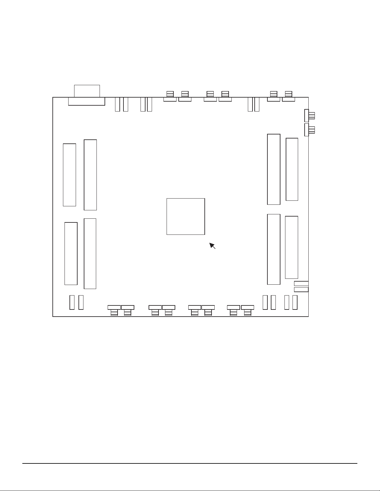
1.2 Description The EV8AQ160-EB Evaluation Board is very straightforward as it implements e2v
EV8AQ160 Quad 8-bit 1.25 Gsps ADC device, Atmel ATMEGA128 AVR, SMA connec-
tors for the sampling clock, analog inputs and reset inputs accesses and 2.54 mm pitch
connectors compatible with high-speed acquisition system probes.
Thanks to its user-friendly interface, the EV8AQ160-EB Kit enables to test all the func-
tions of the EV8AQ160 Quad 8-bit 1.25 Gsps ADC using the SPI connected to a PC.
To achieve optimal performance, the EV8AQ160-EB Evaluation Board was designed in
a 6-metal-layer board using FR4 HTG epoxy dielectric material (200 µm, ISOLA IS410
featuring a resin content of 45%). The board implements the following devices:
The Quad 8-bit 1.25 Gsps ADC Evaluation Board with the EV8AQ160 ADC soldered
SMA connectors for CLK, CLKN, AAI, AAIN, BAI, BAIN, CAI, CAIN, DAI, DAIN,
SYNCP, SYNCN, CAL, CALN signals
2.54 mm pitch connectors for the digital outputs, compatible with high speed
acquisition system probes
Banana jacks for the power supply accesses, the die junction temperature monitoring
functions, reference resistor, analog input common mode voltage (2 mm)
An RS-232 connector for PC interface

Introduction
1-4 EV8AQ160-EB - User Guide
0834E–BDC–07/09
e2v semiconductors SAS 2009
The board dimensions are 170 mm x 185 mm.
The board comes fully assembled and tested, with the EV8AQ160 installed.
Figure 1-1. EV8AQ160-EB Evaluation Board Simplified Schematic
As shown in Figure 1-1, different power supplies are required:
VCC = 3.3V analog positive power supply (includes the SPI pads)
VCCD = 1.8V digital positive power supply
VCCO = 1.8V output power supply
3.3V digital interface primary power supply for the microcontroller
C
H
P
O
R
T
D
H
P
O
R
T
D
L
P
O
R
T
C
L
P
O
R
T
A
H
P
O
R
T
B
H
P
O
R
T
B
L
P
O
R
T
A
L
P
O
R
T
RS232
AAIAAINBAI
BAIN
CAICAINDAIDAIN
GND
VCC
CMIREFAB
CMIREFCD GND
VCCO
VCCD
GND
CALN CAL
DiodA
DiodC
SYNCP SYNCN
CLKN CLK
Res50
Res62
3.3V GND
CAL
CALN
EV8AQ160

EV8AQ160-EB - User Guide 2-5
0834E–BDC–07/09
e2v semiconductors SAS 2008
Section 2
Hardware Description
2.1 Board Structure In order to achieve optimum full-speed operation of the EV8AQ160 Quad 8-bit 1.25
Gsps ADC, a multilayer board structure was retained for the evaluation board. Six cop-
per layers are used, dedicated to the signal traces, ground planes and power supply
planes.
The board is made in FR4 HTG epoxy dielectric material (ISOLA IS410).
The following table gives a detailed description of the board's structure.
Table 2-1. Board Layer Thickness Profile
Layer Characteristics
Layer 1
Copper layer
Copper thickness = 40 µm (with NiAu finish)
AC signals traces = 50Ωmicrostrip lines
DC signals traces
FR4 HTG/dielectric layer Layer thickness = 200 µm
Layer 2
Copper layer
Copper thickness = 18 µm
Upper ground plane = reference plane
FR4 HTG/dielectric layer Layer thickness = 349 µm
Layer 3
Copper layer
Copper thickness = 18 µm
Power plane = VCC
FR4 HTG/dielectric layer Layer thickness = 350 µm
Layer 4
Copper layer
Copper thickness = 18 µm
Power planes = VCCD’ VCCO and 3V3
FR4 HTG/dielectric layer Layer thickness = 350 µm
Layer 5
Copper layer
Copper thickness = 18 µm
Power planes = reference plane (identical to layer 3)
FR4 HTG/dielectric layer Layer thickness = 200 µm
Layer 6
Copper layer
Copper thickness = 40 µm (with NiAu finish)
AC signals traces = 50Ωmicrostrip lines
DC signals traces

Hardware Description
2-6 EV8AQ160-EB - User Guide
0834E–BDC–07/09
e2v semiconductors SAS 2009
The board is 1.6 mm thick.
The Clock, analog inputs, resets, digital data output signals (port H) and ADC functions
occupy the top metal layer, while the output data of the L ports and the SPI signals and
circuitry occupy the bottom layer.
The ground planes occupy layer 2 and 5.
Layer 3 and 4 are dedicated to the power supplies.
2.2 Analog
Inputs/Clock
Input
The differential clock and analog inputs are provided by SMA connectors (Reference:
VITELEC 142-0701-8511).
Both pairs are AC coupled using 10 nF capacitors.
Special care was taken for the routing of the analog and clock input signals for optimum
performance in the high frequency domain:
50Ωlines matched to ±0.1 mm (in length) between XAI and XAIN (X = A, B, C or D) or
CLK and CLKN
909 µm pitch between the differential traces
1270 µm between two differential pairs
361 µm line width
40 µm thickness
850 µm diameter hole in the ground layer below the XAI and XAIN or CLK and CLKN
ball footprints
Figure 2-1. Board Layout for the Differential Analog and Clock Inputs
Note: The analog inputs and clock inputs are AC coupled with 10 nF very close to the SMA
connectors.
2.3 Digital Output The digital output lines were designed with the following recommendations:
50Ωlines matched to ±2.5 mm (in length) between signal of the same differential pair
±1mm line length difference between signals of two differential pairs
635 µm pitch between the differential traces
650 µm between two differential pairs
310 µm line width
40 µm thickness
FR4 HTG
909 µm
1270 µm
e = 40 µm
361 µm 361 µm
200µm

Hardware Description
EV8AQ160-EB - User Guide 2-7
0834E–BDC–07/09
e2v semiconductors SAS 2009
Figure 2-2. Board Layout for the Differential Digital Outputs
The digital outputs are compatible with LVDS standard. They are on-board 100Ωdiffer-
entially terminated as described in Figure 2-3.
Figure 2-3. Differential Digital Outputs Implementation
Double row 2.54 mm pitch connectors are used for the digital output data. The upper
row is connected to the signal while the lower row is connected to Ground, as illustrated
in Figure 2-4.
Figure 2-4. Differential Digital Outputs 2.54 mm Pitch Connector (X = AL, AH, BL, BH,
CL, CH, DL, DH)
2.4 Reset Inputs Two hardware reset signals are provided:
– SYNCP, SYNCN corresponds to the reset of the output clock of the ADC
(analog reset).
– RSTN corresponds to the reset of the SPI (makes the SPI registers go to their
default value).
The differential reset inputs SYNC, SYNCN are provided by SMA connectors (refer-
ence: VITELEC 142-0701-8511).The signals are AC coupled using 10 nF capacitors
and pulled up and down via 200Ωresistors. A variable resistor of 500Ωis implemented
on SYNC: by adjusting this resistor value one can activate and deactivate easily the
reset signal.
FR4 HTG
325 µm
635 µm
e = 40 µm
310 µm 310 µm
200 µm
650 µm
100Ω
Connector ADC
XDR XDRN XD0 XD0N XD7 XD7N XORN
N
XOR
GND GND GND GND GND GND GND GND

Hardware Description
2-8 EV8AQ160-EB - User Guide
0834E–BDC–07/09
e2v semiconductors SAS 2009
50Ωlines matched to ±0.1 mm (in length) between SYNCP and SYNCN
909 µm pitch between the differential traces
1270 µm between two differential pairs
361 µm line width
40 µm thickness
Figure 2-5. Board Layout for the SYNC Signal
Figure 2-6. SYNC, SYNCN Inputs Implementation
The resistors are used only for pull-up and pull-down of the SYNC signals. A push but-
ton is provided for the RSTN reset, as described in Figure 2-7 on page 2-9. This reset
can also be generated through the AVR (via the User Interface).
FR4 HTG
909 µm
1270 µm
e = 40 µm
361µm 361µm
200 µm
SYNC (AC11)
SYNCN (AD11)
500
3.3V
200
SYNC
SYNCN
10 nF
10 nF
3.3V
200
Ω
GND
200
GND
Ω
Ω
Ω
EV8AQ160

Hardware Description
EV8AQ160-EB - User Guide 2-9
0834E–BDC–07/09
e2v semiconductors SAS 2009
Figure 2-7. RSTN Input Implementation
2.5 Power Supplies Layers 3 and 4 are dedicated to power supply planes (VCC, VCCD, VCCO and 3.3V).
The supply traces are low impedance and are surrounded by two ground planes (layer 2
and 5).
Each incoming power supply is bypassed at the banana jack by a 1 µF Tantalum capac-
itor in parallel with a 100 nF chip capacitor.
Each power supply is decoupled as close as possible to the EV8AQ160 device by 10 nF
in parallel with 100 pF surface mount chip capacitors.
Note: The decoupling capacitors are superimposed with the 100 pF capacitor mounted first.
RSTN (AC15)
10KΩ
3.3V
0
GND
0To AVR
Ω
Ω
EV8AQ160

Hardware Description
2-10 EV8AQ160-EB - User Guide
0834E–BDC–07/09
e2v semiconductors SAS 2009

EV8AQ160-EB - User Guide 3-11
0834E–BDC–07/09
e2v semiconductors SAS 2009
Section 3
Operating Characteristics
3.1 Introduction This section describes a typical configuration for operating the evaluation board of the
EV8AQ160 Quad 8-bit 1.25 Gsps ADC.
The analog input signals and the sampling clock signal should be accessed in a differ-
ential fashion. Band pass filters should also be used to optimize the performance of the
ADC both on the analog input and on the clock.
It is necessary to use a very low jitter source for the clock signal (recommended maxi-
mum jitter = 50 ps).
Note: The analog inputs and clock are AC coupled on the board.
3.2 Operating
Procedure
1. Install the SPI software as described in section 4 Software Tools.
2. Connect the power supplies and ground accesses through the dedicated banana
jacks. VCC = 3.3V, VCCD = 1.8V, VCCO = 1.8V and 3.3V.
3. Connect the clock input signals. Use a very low-phase noise High Frequency
generator as well as a band pass filter to optimize the clock performance. The
clock input level is typically 3 dBm and should not exceed 10 dBm (into 50Ω) The
clock frequency should be set to 2.5 GHz (corresponding to 1.25 Gsps sampling
in 4-channel mode or 2.5 Gsps sampling in 2-channel mode or 5 Gsps sampling
in 1-channel mode).
4. Connect the analog input signals (the board has been designed to allow only AC
coupled analog inputs). Use a low-phase noise High Frequency generator as
well as a band pass filter to optimize the analog input performance. The analog
input Full Scale is 500mV peak-to-peak around zero (analog input providing the
Input common mode). It is recommended to use the ADC with an input signal of
-1 dBFS max (to avoid saturation of the ADC).
5. Connect the high speed acquisition system probes to the output connectors. The
digital data are differentially terminated on-board (100Ω) however, they can be
probed either in differential or in single-ended mode.
6. Connect the PC's RS-232 connector to the evaluation board's serial interface.
7. Switch on the ADC power supplies (recommended power up sequence: simulta-
neous or in the following order: VCC = 3.3V, VCCD = 1.8V, VCCO = 1.8V and 3.3V).
8. Turn on the RF clock generator.
9. Turn on the RF signal generator.

Operating Characteristics
3-12 EV8AQ160-EB - User Guide
0834E–BDC–07/09
e2v semiconductors SAS 2009
10. Perform an analog reset (SYNC potentiometer) on the device.
11. Launch Quad-8bit.exe software.
The EV8AQ160-EB evaluation board is now ready for operation.
3.3 Electrical
Characteristics
For more information, please refer to the device datasheet.
Typical conditions:
VCC = 3.3V, VCCD = 1.8V, VCCO = 1.8V
VIN -VINN = 500 mVpp Full Scale differential input, digital outputs LVDS (100Ω)
Tamb (typical) = 25°C unless otherwise specified
Table 3-1. Recommended Conditions of Use
Parameter Symbol Comments Recommended Unit
Analog supply voltage (includes the SPI pads
supply) VCC
Analog core and SPI
pads 3.3 V
Digital supply voltage VCCD Digital parts 1.8 V
Output supply voltage VCCO Output buffer 1.8 V
Differential analog input voltage (Full Scale)
VIN, VINN
VIN -VINN
±250
500 mVpp
Differential Clock input level with 200 fs rms jitter Vinclk 0dBm
Operating temperature range Tamb Commercial Cgrade 0°C < Tamb < 70°C °C
Maximum Operating Junction Temperature TJ125 °C

Operating Characteristics
EV8AQ160-EB - User Guide 3-13
0834E–BDC–07/09
e2v semiconductors SAS 2008
Table 3-2. Electrical Characteristics
Parameter Symbol
Test
Level Min Typ Max Unit Notes
Resolution 8Bit
Power Requirements
Power supply voltage
Analog and SPI pads
Digital
Output
VCC
VCCD
VCCO
3.15
1.7
1.7
3.3
1.8
1.8
3.45
1.9
1.9
V
V
V
Power supply current (DMUX 1:1)
Analog and SPI pads
Digital
Output
ICC
ICCD
ICCO
1.4 1.175
4.9
178
1.3
5.5
200
A
mA
mA
Power supply current (DMUX 1:2)
Analog and SPI pads
Digital
Output
ICC
ICCD
ICCO
1.4 1.25
4.9
300
1.35
5.5
350
A
mA
mA
Power supply current (full standby mode,
DMUX 1:1)
Analog and SPI pads
Digital
Output and 3-Wire serial interface
ICC
ICCD
ICCO
1, 4 136
4.9
29
150
5.5
45
mA
mA
mA
Power supply current (full standby mode,
DMUX 1:2)
Analog and SPI pads
Digital
Output and 3-Wire serial interface
ICC
ICCD
ICCO
1, 4 136
4.9
37
150
5.5
45
mA
mA
mA
Power supply current (partial standby
mode, DMUX 1:1)
Analog and SPI pads
Digital
Output and 3-Wire serial interface
ICC
ICCD
ICCO
1, 4
630
4.9
102
700
5.5
200
mA
mA
mA
Power supply current (partial standby
mode, DMUX 1:2)
Analog and SPI pads
Digital
Output and 3-Wire serial interface
ICC
ICCD
ICCO
1, 4 660
4.9
169
750
5.5
200
mA
mA
mA
Power dissipation (max. power supplies)
Full power (DMUX 1:1)
Full power (DMUX 1:2)
Partial standby (DMUX 1:1)
Partial standby (DMUX 1:2)
Full standby (DMUX 1:1)
Full standby (DMUX 1:2)
PD
1, 4
4.2
4.7
2.3
2.5
0.51
0.525
4.5
4.9
2.45
2.8
0.59
0.59
W
W
W
W
W
W

Operating Characteristics
3-14 EV8AQ160-EB - User Guide
0834E–BDC–07/09
e2v semiconductors SAS 2009

EV8AQ160-EB - User Guide 4-15
0834E–BDC–07/09
e2v semiconductors SAS 2009
Section 4
Software Tools
4.1 Overview The Quad 8-bit 1.25 Gsps ADC Evaluation user interface software is a Visual C++®
compiled graphical interface that does not require a licence to run on a Windows®NT®
and Windows®2000/98/XP®PC.
The software uses intuitive push-buttons and pop-up menus to write data from the
hardware.
4.2 Configuration The advised configuration for Windows®98 is:
PC with Intel®Pentium®Microprocessor of over 100 MHz
Memory of at least 24 Mo
For other versions of Windows®OS, use the recommended configuration from
Microsoft.
Note: Two COM ports are necessary to use two boards simultaneously.
4.3 Getting Started 1. Install the ADC Quad 8-bit application on your computer by launching the
Quad_ADC_8bit_x.x.x.exe installer (please refer to the latest version available).
The screen shown in Figure 4-3 is displayed.

Software Tools
4-16 EV8AQ160-EB - User Guide
0834E–BDC–07/09
e2v semiconductors SAS 2009
Figure 4-1. Install Window
Figure 4-2. QUAD 8-bit 1.25 Gsps Application Setup Wizard Window

Software Tools
EV8AQ160-EB - User Guide 4-17
0834E–BDC–07/09
e2v semiconductors SAS 2009
2. Select Destination Directory
Figure 4-3. QUAD 8-bit 1.25 Gsps Select Destination Directory Window
3. Select Components (choose Full installation)
Figure 4-4. QUAD 8-bit 1.25 Gsps Select Component Window

Software Tools
4-18 EV8AQ160-EB - User Guide
0834E–BDC–07/09
e2v semiconductors SAS 2009
4. Select Start Menu Folder
Figure 4-5. QUAD 8-bit 1.25 Gsps Select Start Menu Window
5. Select Additional Tasks
Figure 4-6. QUAD 8-bit 1.25 Gsps Select Additional Task Window
Table of contents
Other e2v Motherboard manuals