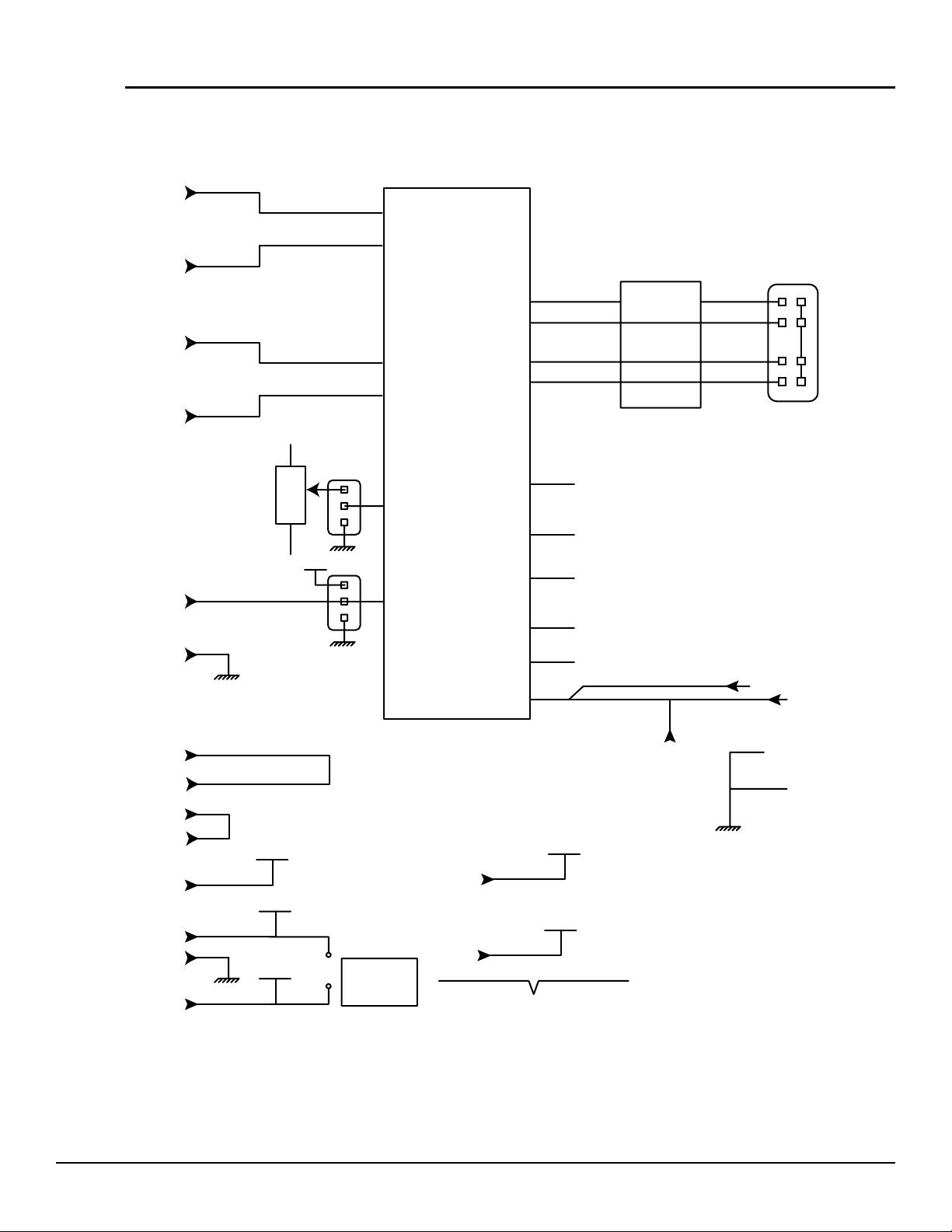
e2v TSEV8308500 User manual

TSEV8308500 Evaluation Board
..............................................................................................
User Guide


TSEV8308500 Evaluation Board User Guide -i
0968D–BDC–01/09
e2v semiconductors SAS 2009
Table of Contents
Section 1
Overview............................................................................................... 1-1
1.1 Description ................................................................................................1-1
1.3 Board Mechanical Characteristics ............................................................1-3
1.4 Analog Input, Clock Input and De-embedding Fixture Accesses..............1-4
1.5 Digital Outputs Accesses ..........................................................................1-4
1.6 Power Supplies and Ground Accesses.....................................................1-4
1.7 ADC Functions Settings Accesses ...........................................................1-4
Section 2
Layout Information ................................................................................ 2-1
2.1 Board ........................................................................................................2-1
2.2 AC Inputs/Digital Outputs..........................................................................2-1
2.3 DC Functions Settings ..............................................................................2-1
2.4 Power Supplies .........................................................................................2-2
2.5 Board Implementation...............................................................................2-2
Section 3
Operating Procedures and
Characteristics ...................................................................................... 3-1
3.1 Introduction ...............................................................................................3-1
3.2 Operating Procedure.................................................................................3-1
3.3 Electrical Characteristics...........................................................................3-2
Section 4
Application Information ......................................................................... 4-1
4.1 Introduction ...............................................................................................4-1
4.2 Analog Inputs ............................................................................................4-1
4.3 Clock Inputs ..............................................................................................4-1
4.4 Setting the Digital Output Data Format .....................................................4-1
4.5 ADC Gain Adjust.......................................................................................4-2
4.6 SMA Connectors and Microstrip Lines De-embedding Fixture .................4-2
4.7 Temperature Monitoring and Data Ready Reset Function .......................4-3
4.8 Data Ready Output Signal Reset..............................................................4-4

-ii TSEV8308500 Evaluation Board User Guide
0968D–BDC–01/09
e2v semiconductors SAS 2009
4.9 Test Bench Description.............................................................................4-5
Section 5
Package Description............................................................................. 5-1
5.1 TS8308500GL Pinout ...............................................................................5-1
5.2 Thermal Characteristics ............................................................................5-3
Section 6
Schematics ........................................................................................... 6-1
6.1 TSEV8308500 Electrical Schematics .......................................................6-1
6.2 Evaluation Board Schematics ...................................................................6-4

TSEV8308500 Evaluation Board User Guide 1-1
0968D–BDC–01/09
e2v semiconductors SAS 2009
Section 1
Overview
1.1 Description The TSEV8308500 Evaluation Board (EB) is a prototype board which has been
designed in order to facilitate the evaluation and the characterization of the TS8308500
device up to its 1.3 GHz full analog power bandwidth at up to 500 Msps in the extended
temperature range.
The high speed sampling rate of the TS8308500 requires careful attention to circuit
design and layout to achieve optimal performance. This four metal layer board with
internal ground plane has the adequate functions in order to allow a quick and simple
evaluation of the TS8308500 ADC performances over the temperature range.
The TS8308500 Evaluation Board (EB) is very straightforward as it only implements the
TS8308500 ADC device, SMA connectors for input/output accesses and a 2.54 mm
pitch connector compatible with standard high frequency probes.
The board also implements a de-embedding fixture in order to facilitate the evaluation of
the high frequency insertion loss of the inputs microstrip lines, and a die junction tem-
perature measurement setting.
The board is constituted by a sandwich of two dielectric layers, featuring low insertion
loss and enhanced thermal characteristics for operation in the high frequency domain
and extended temperature range.
The board dimensions are 130 mm x 130 mm.
The board set comes fully assembled and tested, with the TS8308500 installed and
heatsink.

Overview
1-2 TSEV8308500 Evaluation Board User Guide
0968D–BDC–01/09
e2v semiconductors SAS 2009
1.2 TSEV8308500
Evaluation Board
Figure 1-1. TSEV8308500 Block Diagram
CLK
CLKB
Differential
Clock inputs
Z0 = 50
Z0 = 50
CLK
CLKB
TS8308500
VIN
VINB
Differential
Clock inputs
Z0 = 50
Z0 = 50
VIN
VINB
ADC Gain Adjust
GAIN/GND
VCC
GORB GORB
DR/DRB
D0/D0B
Z0 = 50
Z0 = 50
Z0 = 50
Z0 = 50
D7/D7B
OR/ORB
VCC VCC = +5V
GND
VPLUSD
GND = 0V
VPLUSD = 0V (ECL)
VPLUSD = 2.4V (LVDS)
AVEE
DVEE
DIOD/DRRB
VEEA = -5V
VEED = -5V
J - diode
V - diode
DRRB V-GND
V-GND
(Deembedding fixture)
CAL1
CAL2
CAL3
CAL4
L = 65 mm typ = LVIN/VINb
= LCLK/CLKb
L = 18 mm typ
+5V
VCC
-5V
VEET
-2V
VDD
-5V
VEEA
GND -5V
VEED
Short-circuit
possibility
here MC100EL 16 SUPPLIES

Overview
TSEV8308500 Evaluation Board User Guide 1-3
0968D–BDC–01/09
1.3 Board
Mechanical
Characteristics
The board layer’s number, thickness, and functions are given below, from top to bottom.
The TSEV8308500 is a seven-layer PCB constituted by four copper layers and three
dielectric layers.
The four metal layers correspond respectively from top to bottom to the AC and DC sig-
nals layer (layer 1), two ground layers (layers 3 and 5), and one supply layer (layer 7).
The upper inner ground plane (layer 3) constitutes the reference plane for the 50Ω
impedance signal traces. The lower inner ground plane (layer 5) is used for dielectric
substrate rigidity and is a replica of the upper ground plane.
The backside metal layer is dedicated to the power supplies planes, surrounded by a
ground plane.
The three dielectric layers are respectively (from top to bottom) constituted by a low
insertion loss dielectric layer (RO4003) (layer 2) and two parallel BT/Epoxy dielectric
layers (layers 4 and 6).
Considering the severe mechanical constraints due to the wide temperature range and
the high frequency domain in which the board is to operate, it is necessary to use a
sandwich of two different dielectric materials, with specific characteristics:
A low insertion loss RO4003 Hydrocarbon/wovenglass dielectric layer of 200 µm
thickness, chosen for its low loss (-0.318 dB/inch) and enhanced dielectric
consistency in the high frequency domain. The RO4003 dielectric layer is dedicated to
the routing of the 50Ωimpedance signal traces (the RO4003 typical dielectric
constant is 3.4 at 10 GHz). The RO4003 dielectric layer characteristics are very close
to PTFE in terms of insertion loss characteristics.
A BT/Epoxy dielectric layer of 2 mm total thickness which is sandwiched between the
upper ground plane and the back-side supply layer.
Table 1-1. Board Layers Thickness Profile
Layer Characteristics
Layer 1
Copper layer
Copper thickness = 35 µm
AC signals traces = 50Ωmicrostrip lines
DC signals traces (GORB, GAIN, DIODE)
Layer 2
RO4003 dielectric layer
(Hydrocarbon/Wovenglass)
Layer thickness = 200 µm
Dielectric constant = 3.4 at 10 GHz
-0.044 dB/inch insertion loss at 2.5 GHz
-0.318 dB/inch insertion loss at 18 GHz
Layer 3
Copper layer
Copper thickness = 35 µm
Upper ground plane = reference plane 50Ωmicrostrip return
Layer 4
BT/Epoxy dielectric layer
Layer thickness = 630 mm
Layer 5
Copper layer
Copper thickness = 35 µm
Lower ground plane (board mechanical rigidity)
Layer 6
BT/Epoxy dielectric layer
Layer thickness = 630 mm
Layer 7
Copper layer
Copper thickness = 35 µm
Power planes = VEEA, VEED, VEET
, VDD, VCC, VPLUSD ground plane

Overview
1-4 TSEV8308500 Evaluation Board User Guide
0968D–BDC–01/09
e2v semiconductors SAS 2009
The BT/Epoxy layer has been chosen because of its enhanced mechanical characteris-
tics for elevated temperature operation. The typical dielectric constant is 4.5 at 1 MHz.
More precisely, the BT/Epoxy dielectric layer offers enhanced characteristics compared
to FR4 Epoxy, namely:
Higher operating temperature value: 170°C (125°C for FR4).
Better with standing of thermal shocks (-65°C up to 170°C).
The total board thickness is 1.6 mm. The previously described mechanical and fre-
quency characteristics makes the board particularly suitable for the device evaluation
and characterization in the high frequency domain and in the military temperature range.
1.4 Analog Input,
Clock Input and
De-embedding
Fixture Accesses
The differential active inputs (Analog, Clock, De-embedding fixture) are provided by
SMA connectors.
Reference: VITELEC 142-0701-851.
1.5 Digital Outputs
Accesses
Access to the differential output data port is provided by a 2.54 mm pitch connector,
compatible with standard Digital Acquisition System. It enables access to the converter
output data, as well as proper 50Ωdifferential termination.
1.6 Power Supplies
and Ground
Accesses
The power supplies accesses are provided by five 4 mm section banana jacks respec-
tively for VEEA, VEED, VEET, VDD, VPLUSD and VCC.
The Ground accesses are provided by 4 mm and two 2 mm banana jacks.
1.7 ADC Functions
Settings
Accesses
For ADC functions settings accesses (GORB, Die junction temp., ADC gain adjust),
smaller 2 mm section banana jacks are provided.
A potentiometer is provided for ADC gain adjust.

TSEV8308500 Evaluation Board User Guide 2-1
0968D–BDC–01/09
e2v semiconductors SAS 2009
Section 2
Layout Information
2.1 Board The TS8308500 requires proper board layout for optimum full speed operation.
The following explains the board layout recommendations and demonstrates how the
Evaluation Board fulfills these implementation constraints.
A single low impedance ground plane is recommended, since it allows the user to lay
out signal traces and power planes without interrupting the ground plane.
Therefore a multi-layer board structure has been retained for the TSEV8308500.
Four copper metal layers are used, dedicated respectively (from top to bottom) to the
signal traces, ground planes and power supplies.
The input/output signal traces occupy the top metal layer.
The ground planes occupy the second and third copper metal layers.
The bottom metal layer is dedicated to the power supplies.
2.2 AC Inputs/Digital
Outputs
The board uses 50Ωimpedance microstrip lines for the differential analog inputs, clock
inputs, and differential digital outputs (including the Out of Range Bit and the data ready
output signal).
The input signals and clock signals must be routed on one layer only, without using any
through-hole vias. The line lengths are matched to within 2 mm. The analog and clock
input lines are properly reverse terminated by 50Ωsurface mount chip resistors placed
very close to the ADC device.
The digital output lines are 50Ωdifferentially terminated.
The output data traces lengths are matched to within 0.25 inch (6 mm) to minimize the
data output delay skew.
For the TSEV8308500 the propagation delay is approximately 6.1 ps/mm (155 ps/inch).
The RO4003 typical dielectric constant is 3.4 at 10 GHz.
For more informations about different output termination options, refer to the specifica-
tion application notes.
2.3 DC Functions
Settings
The DC signals traces are low impedance. They have been routed with 50Ωimpedance
near the device because of room restriction.

Layout Information
2-2 TSEV8308500 Evaluation Board User Guide
0968D–BDC–01/09
e2v semiconductors SAS 2009
2.4 Power Supplies The bottom metal layer 7 is dedicated to the power supply traces (VEEA, VEED, VEET, VCC,
VDD, VPLUSD).
The supply traces are approximately 6 mm wide in order to present low impedance, and
are surrounded by a ground plane connected to the two inner ground planes.
The Analog and Digital negative power supply traces are independent, but the possibil-
ity exists to short-circuit both supplies on the top metal layer.
No difference in ADC high speed performance is observed when connecting both nega-
tive supply planes together. Obviously one single negative supply plane could be used
for the circuit.
Each power supply incoming is bypassed by a 1 µF Tantalum capacitor in parallel with
1 nF chip capacitor.
Each power supply access is decoupled very close to the device by a 10 nF and 100 pF
surface mount chip capacitors in parallel.
Note: The decoupling capacitors are superposed. In this configuration, the 100 pF capacitors
must be mounted first.
2.5 Board
Implementation
Surface-mount resistors and chip capacitors allow the closest possible connections to
the device pins, for microstrip line back termination and bypassing.
Connecting the positive supply pads:
– The positive supply pads denoted VCC:
The corresponding VCC pad numbers are 19, 21, 23, 30, 39, 40.
Each VCC power supply pad is decoupled as closely to the device as possible
by a 10 nF and 100 pF chip capacitor.
The VCC supply pads are connected to the back side VCC plane of the CEB.
– The positive digital supply pads are denoted VPLUSD (0V or 2.4V).
The corresponding VPLUSD pad numbers are 1, 11.
Each VPLUSD power supply pad is decoupled very close to the device by a
10 nF and 100 pF chip capacitor.
The VPLUSD supply pads are connected to the back side VPLUSD plane of the
evaluation board.
Connecting the negative supply pads:
– The TS8308500 has separate analog and digital -5V supplies:
The negative analog supply pads are denoted VEE.
The VEE corresponding pad numbers are 22, 29, 31.
The negative digital supply pad is denoted DVEE.
The DVEE corresponding pad number is pad 6.
The DVEE supply pad is dedicated to the digital output buffers only.
Each VEE and DVEE power supply pad is decoupled as closely as possible
near the device by a 10 nF and 100 pF chip capacitor.
–TheV
EE and DVEE supply pads are respectively connected to the backside
layer 7 VEE and VEED supply planes.
Ground pads connections:
– The analog ground pads are denoted GND.
The corresponding GND pad numbers are 20, 26, 28, 33, 35, 37.

TSEV8308500 Evaluation Board User Guide 3-1
0968D–BDC–01/09
e2v semiconductors SAS 2009
Section 3
Operating Procedures and
Characteristics
3.1 Introduction This section describes a typical single-ended configuration for analog inputs and clock
inputs.
The single-ended configuration is preferable, as it corresponds to the most straightfor-
ward and quickest TSEV8308500 board setting for evaluating the TS8308500 at full
speed in the military temperature range.
The inverted analog input VINB and clock input CLKB common mode level is Ground
(on-board 50Ωterminated). In this configuration, no balun transformer is needed to con-
vert properly single-ended mixer output to balanced differential signals for the analog
inputs.
In the same way, no balun is necessary to feed the TS8308500 clock inputs with bal-
anced signals.
Connect directly the RF sources to the in-phase analog and clock inputs of the
converter.
However, dynamic performances can be somewhat improved by entering either analog
or clock inputs in differential mode.
3.2 Operating
Procedure
1. Connect the power supplies and Ground accesses
(VCC = +5V, GND = 0V, VPLUSD = 0V, VEAE = VEED = -5V) through the dedicated
banana jacks.
The -5V power supplies should be turned on first.
Note: one single -5V power supply can be used for supplying the digital VEED and
analog VEEA power planes.
2. The board is set by default for digital outputs in binary format.
3. Connect the CLK clock signal.
The inverted phase clock input CLKB may be left open (as on-board 50Ωtermi-
nated). Use a low phase noise RF source. The clock input level is typically
4 dBm and should not exceed +10 dBm into the 50Ωtermination resistor (maxi-
mum ratings for clock input power level is 15 dBm). Clock frequency can range
between 10 MHz and 700 MHz.

Operating Procedures and Characteristics
3-2 TSEV8308500 Evaluation Board User Guide
0968D–BDC–01/09
e2v semiconductors SAS 2009
4. Connect the analog signal VIN. The inverted phase clock input VINB may be left
open (as on-board 50Ωterminated). Use a low phase noise RF source. Full
Scale range is 0.5V peak to peak around 0V, (±250 mV), or -2 dBm into 50Ω.
Input frequency can range from DC up to 1.3 GHz. At 1.3 GHz (TBC), the ADC
attenuates by -3 dB the input signal. The board insertion loss (S21) will be fur-
nished in definitive document release.
5. Connect the high speed data acquisition system probes to the output connector.
The connector pitch (2.54 mm) is compatible with High Speed Digital Acquisition
System probes. The digital data are on-board differentially terminated. However,
the output data can be picked up either in single-ended or differentially mode.
6. Board functionality verification and proposed product evaluation procedure:
– A first test can be run at 500 Msps/250 MHz Nyquist: about 7.1 Effective Bits
(typ) should be obtained.
– At 500 Msps/20 MHz: about 7.2 Effective Bits (typ) should be obtained.
– At 500 Msps/500 MHz and -1 dB Full Scale analog input, 7.0 bits and -52 dBc
SFDR should be obtained.
7. The devices operate respectively from 10 Msps up to 500 Msps in binary output
format and 10 Msps up to 500 Msps in Gray output format. It is capable of sam-
pling analog input waveforms ranging from DC up to 1.3 GHz.
3.3 Electrical
Characteristics
Notes: 1. Absolute maximum ratings are limiting values (referenced to GND = 0V), to be applied individually, while other parameters
are within specified operating conditions. Long exposure to maximum rating may affect device reliability. The use of a ther-
mal heat sink is mandatory.
2. In case only one supply is used for supplying the -5V negative power planes, apply the VEED absolute maximum ratings.
Table 3-1. Absolute Maximum Ratings
Parameter Symbol Comments Value Unit
Positive supply voltage VCC GND to 6 V
Digital negative supply voltage DVEE(2) GND to -5.7 V
Digital positive supply voltage VPLUSD GND -0.3 to 2.8 V
Negative supply voltage VEE(2) GND to -6 V
Maximum difference between negative supply voltages DVEE to VEE 0.3 V
Analog input voltages VIN or VINB -1 to +1 V
Maximum difference between VIN and VINB VIN - VINB -2 to +2 V
Clock input voltage VCLK or VCLKB -3 to +1.5 V
Maximum difference between VCLK and VCLKB VCLK - VCLKB -2 to +2 V
Static input voltage VDGORB -0.3 to VCC +0.3 V
Digital input voltage VDDRRB VEE -0.3 to +0.9 V
Digital output voltage VOVPLUSD -3 to VPLUSD -0.5 V
Maximum junction temperature Tj+145 °C
Storage temperature Tstg -65 to +150 °C
Lead temperature (soldering 10s) Tleads +300 °C

Operating Procedures and Characteristics
TSEV8308500 Evaluation Board User Guide 3-3
0968D–BDC–01/09
3.4 Operating
Characteristics
The power supplies denoted VCC, VEEA, VEED and VPLUSD are dedicated for the
TS8308500 ADC.
The power supplies denoted VEET, VDD are dedicated to the optional MC100EL16 asyn-
chronous differential receivers.
Table 3-2. Electrical Operating Characteristics
Parameter Symbol
Value
UnitMin Typ Max
Positive supply voltage
(dedicated to TS8308500 ADC only)
VCC 4.75 5 5.25 V
VPLUSD
LVDS: 1.4
ECL: 0
LVDS: 2.4 LVDS: 2.6
V
V
VEEA -5.25-5-4.75V
VEED -5.25-5-4.75V
Positive supply current
(dedicated to TS8308500 ADC only)
ICC – 400 425 mA
IPLUSD – 120 130 mA
IEEA – 170 185 mA
IEED – 140 160 mA
Positive supply voltage not used by default – If installed
(dedicated to MC100EL16 differential Receivers)
VEET -5.25-5-4.75V
VDD -2.15 -2 -185 V
Positive supply current not used by default – If installed
(dedicated to MC100EL16 differential Receivers)
IEET – 150 – mA
IDD – 390 – mA
Nominal power dissipation (without receivers) PD – 3.8 3.9
(Tj = 125°C)
W
Analog input impedance ZIN –50–Ω
Full Power Analog Input Bandwidth (-3 dB) – 1.3 1.3 – GHz
Analog Input Voltage range (differential mode) VIN -125 – 125 V
Clock input impedance – – 50 – Ω
Clock inputs voltage compatibility (Single-ended or
differential) (See Application Notes)
– ECL levels or 4 dBm (typ.) into 50Ω–
Clock input power level into 50Ωtermination resistor – -2 4 10 dBm

Operating Procedures and Characteristics
3-4 TSEV8308500 Evaluation Board User Guide
0968D–BDC–01/09
e2v semiconductors SAS 2009

TSEV8308500 Evaluation Board User Guide 4-1
0968D–BDC–01/09
e2v semiconductors SAS 2009
Section 4
Application Information
4.1 Introduction For this section, refer also to the product Specification application notes (TS8308500
Datasheet). More particularly, refer to sections related to single-ended and differential
input configurations.
4.2 Analog Inputs The analog inputs can be entered in differential or single-ended mode without any high
speed performance degradation.
The board digitizes single-ended signals by choosing either input and leaving the other
input open, as the latter is on-board 50Ωterminated. The nominal In-phase inputs are
VIN (See Section 3.2).
4.3 Clock Inputs The clock inputs can be entered in differential or single-ended mode without any high
speed performance degradation. Moreover, the clock input common mode may be 0V,
or -1.3V if ECL input format is used for the clock inputs.
As for the analog input, either clock input can be chosen, leaving the other input open,
as both clock inputs are on-board 50Ωterminated. The nominal in-phase clock input is
CLK (See Section 3).
4.4 Setting the
Digital Output
Data Format
For this section, refer to the Evaluation Board Electrical schematic and to the compo-
nents placement document (respectively Figure 6-1 and Figure 6-7).
Refer also to the TS8308500 specification pages about digital output coding.
The TS8308500 delivers data in natural binary code or in Gray code. If the “GORB”
input is left floating or tied to VCC the data format selected will be natural binary, if this
input is tied to ground the data will follow Gray code.
Use the jumper denoted ST2 for selecting the output data port format:
If ST2 is left floating or tied to VCC, the data output format is true Binary,
If ST2 is tied to GND, the data outputs are in Gray format.

Application Information
4-2 TSEV8308500 Evaluation Board User Guide
0968D–BDC–01/09
e2v semiconductors SAS 2009
The VPLUSD positive supply voltage allows the adjustment of the output common mode
level from -1.2V (VPLUSD = 0V for ECL output compatibility) to +1.2V (VPLUSD = 2.4V for
LVDS output compatibility).
Each output voltage varies between -1.02V and -1.35V (respectively +1.38V and
+1.05V), leading to ±0.33V = 660 mV in differential, around -1.8V (respectively +1.21V)
common mode for VPLUSD = 0V (respectively 2.4V).
4.5 ADC Gain Adjust The ADC gain is adjustable by the means of the pin (60) (pad input impedance is 1 MΩ
in parallel with 2 pF). A jumper denoted ST1 has been foreseen in order to have access
to the ADC gain adjust pin.
The P1 potentiometer is dedicated for adjusting the ADC gain from approximately 0.85
up to 1.15.
The gain adjust transfer function is given below.
Figure 4-1. ADC Gain Adjust
4.6 SMA Connectors
and Microstrip
Lines De-
embedding
Fixture
Attenuation in microstrip lines can be found by taking the difference in the log magni-
tudes of the S21 scattering parameters measured on two different lengths of
meandering transmission lines.
Such a difference measurement also removes common losses such as those due to
transitions and connectors.
The scattering parameter S21 corresponds to the amount of power transmitted through
a two-port network.
The characteristic impedance of the microstrip meander lines must be close to 50Ωto
minimize impedance mismatch with the 50Ωnetwork analyzer test ports.
Impedance mismatch will cause ripple in the S21 parameter as a function of both the
degree of mismatch and the length of the line.
0.80
0.85
0.90
0.95
1.00
1.05
1.10
1.15
1.20
-600 -400 -200 0 200 400 600
Vgain (command voltage) (mV)
ADC Gain

Application Information
TSEV8308500 Evaluation Board User Guide 4-3
0968D–BDC–01/09
4.7 Temperature
Monitoring and
Data Ready
Reset Function
One single pad is used for both DRRB input command and die junction monitoring. The
pad denomination is DRRB/DIOD. Temperature monitoring and Data Ready control by
DRRB is not possible simultaneously.
4.7.1 Die Junction
Temperature
Measurement Setup
For operation in the extended temperature range, forced convection is required, to
maintain the device junction temperature below the specified maximum value
(Tj max = 125°C).
A die junction temperature measurement setting has been included on the board, for
junction temperature monitoring.
Four 2 mm section banana jacks (J9, J10, J11, J12) are provided to force current and
measure the VBE voltage across the dedicated transistor connected between pads 32
and 33.
The measurement method consists of forcing a 3 mA current flowing into a diode
mounted transistor, connected between pad 32 and pad 33 (pad 32 is the emitter and
pad 33 is the shorted base-collector).
CAUTION:
Respect the current source polarity. In any case, make sure the maximum voltage com-
pliance of the current source is limited to maximum 1V or use the resistor mounted in
serial with the current source to avoid damage occurring to the transistor device. This
may occur for instance if current source is reverse connected.
The measurement setup is described in Figure 4-2. The diode VBE forward voltage ver-
sus junction temperature (in steady state conditions) is given in Figure 4-3.
Figure 4-2. TS8308500 Die Junction Temperature Measurement Setup
∅ 2 mm banana connectors
32
33
J12
J11
J10
J9
Pads
I-DIODE
I-GND
V-DIODE
V-GND
NP1032C2

Application Information
4-4 TSEV8308500 Evaluation Board User Guide
0968D–BDC–01/09
e2v semiconductors SAS 2009
Figure 4-3. Transistor VBE Forward Voltage Versus Junction Temperature (I = 3 mA)
4.8 Data Ready
Output Signal
Reset
A subvis connector is provided for DRRB command.
The Data ready signal is reset on falling edge of DRRB input command, on ECL logical
low level (-1.8V). DRRB may also be tied to VEE = -5V for Data Ready output signal
master Reset. As long DRRB as remains at logical low level, (or tied to VEE = -5V), the
Data Ready output remains at logical zero and is independent of the external free run-
ning encoding clock.
The Data ready output signal (DR, DRB) is reset to logical zero after TRDR = 720 ps
typical.
TRDR is measured between the -1.3V point of the falling edge of DRRB input command
and the zero crossing point of the differential Data Ready output signal (DR, DRB).
The Data ready Reset command may be a pulse of 1 ns minimum time width.
The Data ready output signal restarts on DRRB command rising edge, ECL logical high
levels (-0.8V).
DRRB may also be grounded, or is allowed to float, for normal free running Data ready
output signal.
600
640
680
720
760
800
840
880
920
960
1000
-80 -60 -40 -20 0 20 40 60 80 100 120 140
VBE (mV)
Junction temperature (°C)

Application Information
TSEV8308500 Evaluation Board User Guide 4-5
0968D–BDC–01/09
4.9 Test Bench
Description
Figure 4-4. Differential Analog and Clock Inputs Configuration
Figure 4-5. Single-ended Analog and Clock Input Configuration
Signal Generator
Signal Generator
-121 dBc/Hz at 1 Hz
offset from fc
0 −180°
Hybrid
0 −180°
Hybrid
BPF
Data Acquisition
System
TS8308500
ADC
-117 dBc/Hz at 20 Hz
offset from fc
PC
GPIB
CLKB CLK
DR
8 Data
Tunable delay line
-8 dBm
VINB
VIN
-8 dBm
Synchro 10 MHz
BPF
Data Acquisition
System
TS8308500
ADC
PC
GPIB
(50Ω) CLKB CLK (4 dBm)
DR
8 Data
Tunable delay line
VINB
(50Ω)
VIN
-2 dBm
Synchro 10 MHz
Signal Generator
Signal Generator

Application Information
4-6 TSEV8308500 Evaluation Board User Guide
0968D–BDC–01/09
e2v semiconductors SAS 2009
Table of contents
Other e2v Motherboard manuals
Popular Motherboard manuals by other brands

Microchip Technology
Microchip Technology EVB-LAN9252-HBI+ user guide

Gigabyte
Gigabyte GA-X99-SLI user manual

Qiyangtech
Qiyangtech QY-9263S Hardware manual

Asus
Asus TUF GAMING B650-PLUS quick start guide

Analog Devices
Analog Devices ADSP-21160 EZ-KIT Lite System manual

Asus
Asus N3050T R2.0 quick start guide