EV8AQ160-DK
2 BDC- 1-Sep-10
e2v semiconductors SAS 2010
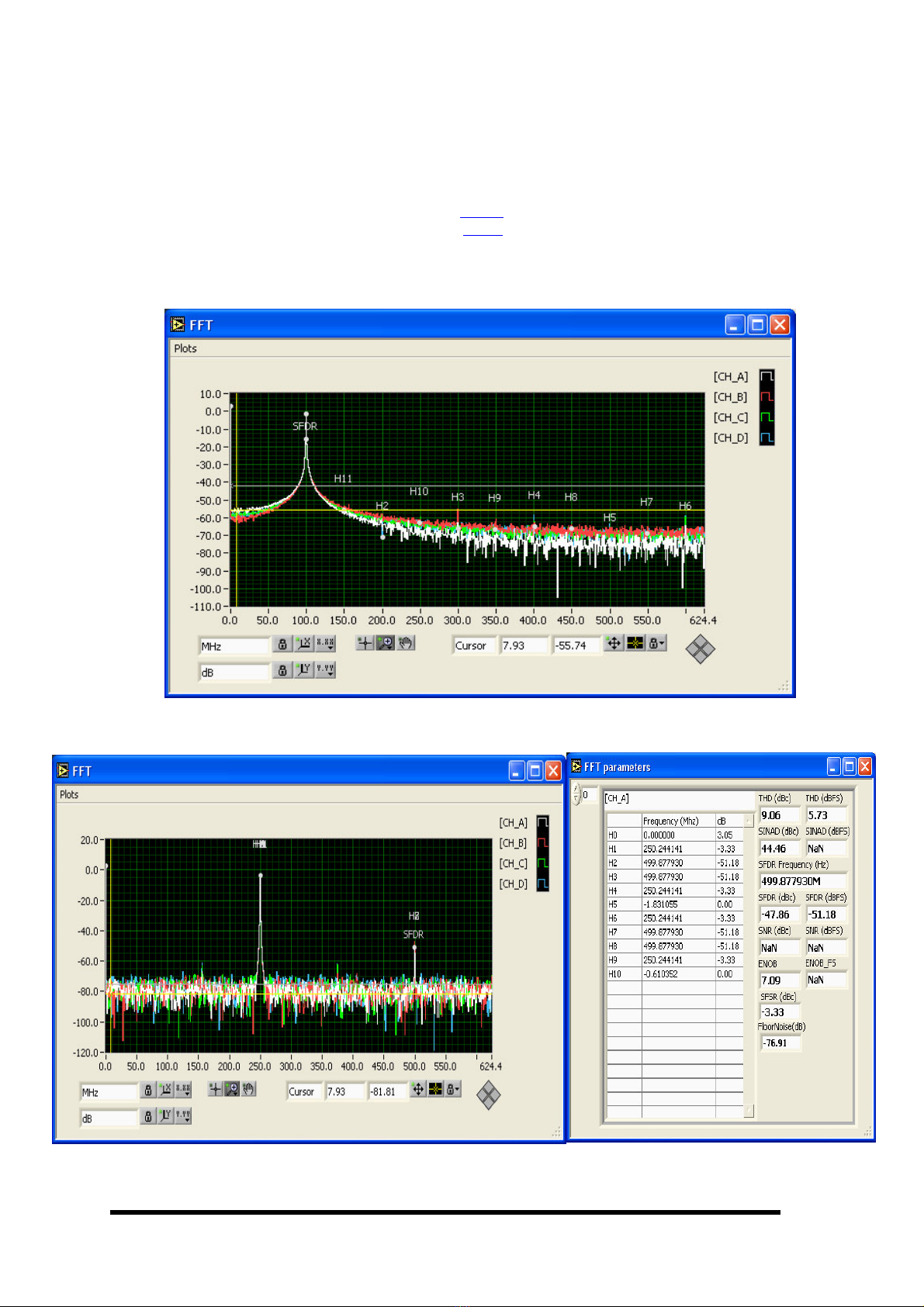
1 General overview
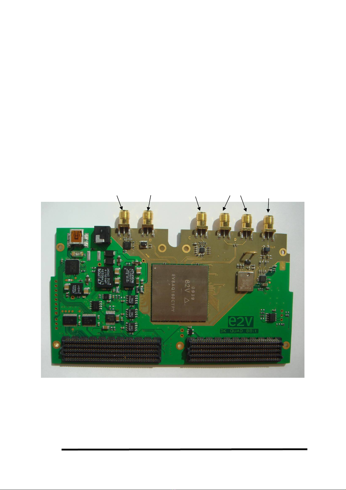
The QUAD 8bit Demo Kit enables the easy evaluation of the characteristics and performance of ADC
QUAD 8bit EV8AQ160. The Demo kit is plug_and_play and needs little external equipment.
The Demo kit is delivered with software which allows acquisition of data using the FPGA.
The QUAD 8bit Demo Kit is compatible with VITA57 FMC (FPGA Mezzanine Card) standard.
For more information please see the VITA site web.
http://www.vita.com/fmc.html
The Demo kit QUAD 8bit is 100% compatible with XILINX VIRTEX 6 evaluation kit ML605
This board is designed for use as a reference design.
All front end devices are fitted including: DC-DC regulator, ADC driver, clock generator….
Please see chap Main Functions
The FPGA VHDL data acquisition code for the ML605 board is supplied.
Please see chap FPGA CODE
1.1. Disclaimer
The information in this document is provided in connection with E2V products.
No license, express or implied, by estoppel or otherwise, to any intellectual property right is granted by
this document or in connection with the sale of E2V products.
EXCEPT AS SET FORTH IN E2V’S TERMS AND CONDITIONS OF SALE LOCATED ON E2V’S
WEB SITE, E2V ASSUMES NO LIABILITY WHATSOEVER AND DISCLAIMS ANY EXPRESS,
IMPLIED OR STATUTORY WARRANTY RELATING TO ITS PRODUCTS INCLUDING, BUT NOT
LIMITED TO, THE IMPLIED WARRANTY OF MERCHANTABILITY, FITNESS FOR A PARTICULAR
PURPOSE, OR NON-INFRINGEMENT. IN NO EVENT SHALL E2V BE LIABLE FOR ANY DIRECT,
INDIRECT, CONSEQUENTIAL, PUNITIVE, SPECIAL OR INCIDENTAL DAMAGES (INCLUDING,
WITHOUT LIMITATION, DAMAGES FOR LOSS OF PROFITS, BUSINESS INTERRUPTION, OR
LOSS OF INFORMATION) ARISING OUT OF THE USE OR INABILITY TO USE THIS DOCUMENT,
EVEN IF E2V HAS BEEN ADVISED OF THE POSSIBILITY OF SUCH DAMAGES.
E2V makes no representations or warranties with respect to the accuracy or completeness of the
contents of this document and reserves the right to make changes to specifications and product
descriptions at any time without notice. E2V does not make any commitment to update the
information.
This kit must be regarded as a tool, not a finished product. It allows you to evaluate the performance of
the e2v component, design prototypes and debug software. It CANNOT be resold as a finished
product that must be compliant with local relevant regulations.
Its function is as a development system, demonstrating the performance of e2v semiconductors
components and not as a final product available on general release.
Since this Development Kit is intended to be used on an industrial workbench and modified by the
user to build his prototypes, NO WARRANTY OF ANY KIND can apply.
NO LIABILITY will be accepted by e2v, whatsoever may arise as a result of the use of these boards.