Hardware Description
2-4 TSEV81102G0FS Evaluation Board User Guide
0974C–BDC–02/09
e2v semiconductors SAS 2009
2.2 Board Structure
2.2.1 Thickness Profile of
Board Layers
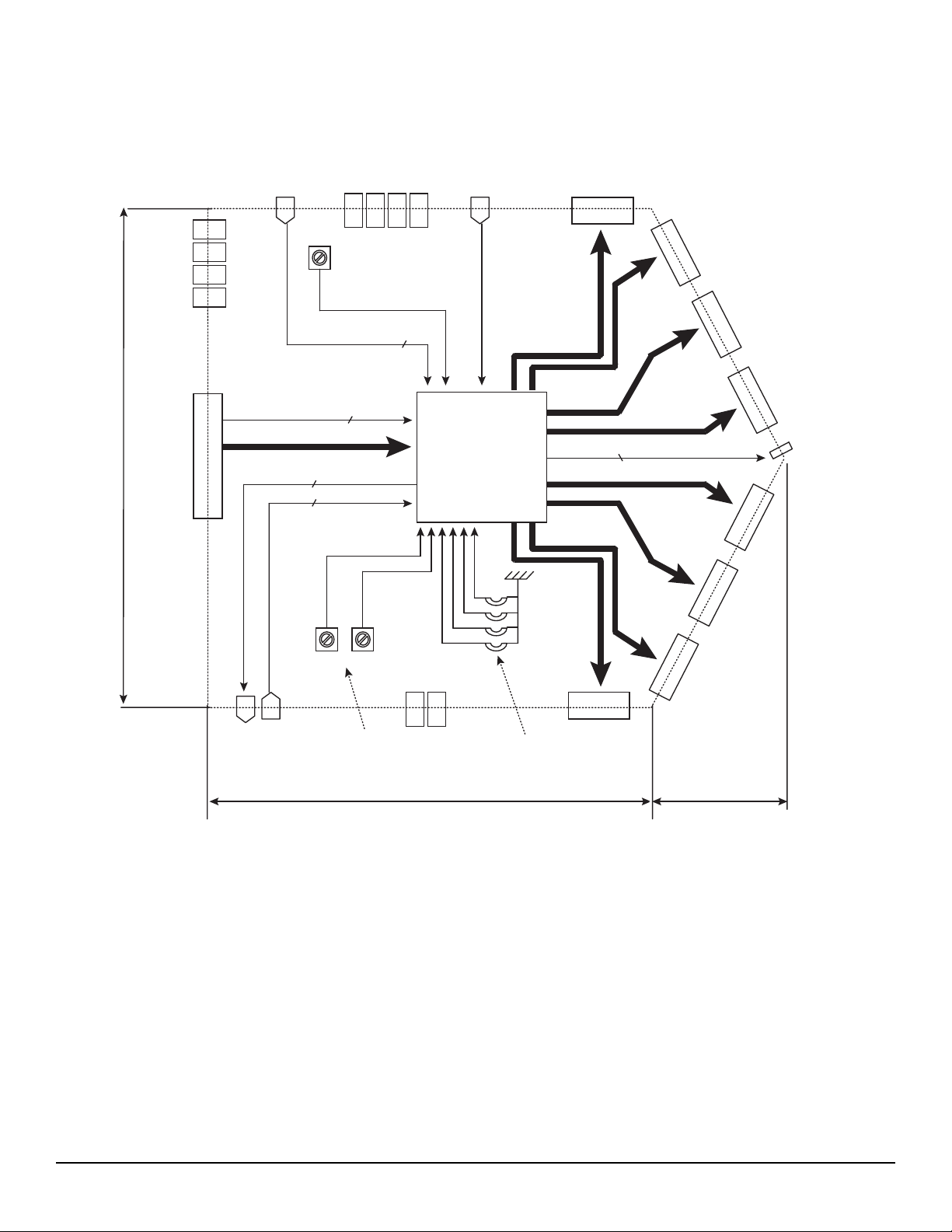
The TSEV81102G0 is a seven-layered PCB constituted of four copper layers and three
dielectric layers.
The board is 1.6 mm thick. The number of layers, thickness and function of each layer,
starting with the top layer, are given in Table 2-1.
2.2.2 Metal Layers The four metal layers respectively correspond to:
The signals’ layer (layer 1)
The two reference layers (layers 3 and 7)
The supply layer (layer 5)
The upper and lower reference planes (layers 3 and 7) are partitioned into GND (the ref-
erence for the input signals) and VPLUSD (the reference for the digital output signals), in
the same way as the DMUX package.
The fifth layer is dedicated to power supplies and to ground.
2.2.3 Dielectric Layers The three dielectric layers are respectively composed of a low insertion loss dielectric
(RO4003) layer (layer 2) and BT/epoxy dielectric layers (layers 4 and 6).
Considering the severe mechanical constraints of the wide temperature range and the
high frequency domain in which the board is meant to operate, two different dielectric
materials are used:
The first is a low insertion loss RO4003 hydrocarbon/wovenglass dielectric (–0.044
dB/inch loss at 2.5 GHz), which has an enhanced dielectric consistency in the high
frequency domain, and is dedicated to the routing of 50Ωand 60Ωtraces. The
RO4003 dielectric constant is typically 3.4 at 10 GHz.
Table 2-1. Board Layer Thickness Profiles
Layer Characteristic
Layer 1
Copper layer
Copper thickness = 35 µm
Input signals: 50Ωmicrostrip lines
Output data signals: 60Ωmicrostrip lines, 50Ωterminated
Layer 2
RO4003 dielectric layer
(Hydrocarbon/wovenglass)
Layer thickness = 200 µm
Dielectric constant = 3.4 at 10 GHz
–0.044 dB/inch loss at 2.5 GHz
–0.018 dB/inch loss at 18 GHz
Layer 3
Copper layer
Copper thickness = 35 µm
Upper reference plane divided into two parts: GND and VPLUSD
Layer 4
BT/epoxy dielectric layer Layer thickness = 0.4 mm
Layer 5
Copper layer
Copper thickness = 35 µm
Power plane: VEE, VCC, VTT
, GND
Layer 6
BT/epoxy dielectric layer Layer thickness = 860 µm
Layer 7
Copper layer
Copper thickness = 35 µm
Lower reference plane