ECS L7VTA3 User manual

L7VTA3 V3.1a
i
Preface
Copyright
This publication, including all photographs, illustrations and software, is protected un-
der international copyright laws, with all rights reserved. Neither this manual, nor any
of the material contained herein, may be reproduced without writtenconsent ofthe au-
thor.
Version 3.1a
Disclaimer
The information in this document is subject to change without notice. The manufac-
turer makes no representations or warranties with respect to the contents hereof and
specifically disclaim any implied warranties of merchantability or fitness for any
particular purpose. The manufacturer reserves the right to revise this publication and
to make changes from time to time in the content hereof without obligation of the
manufacturer to notify any person of such revision or changes.
Trademark Recognition
Microsoft, MS-DOS and Windows are registered trademarks of Microsoft Corp.
MMX, Pentium, Pentium-II, Pentium-III, Celeron are registered trademarks of Intel
Corporation.
Other product names used in this manual are the properties of their respective owners
and are acknowledged.
Federal Communications Commission (FCC)
This equipment has been tested and found to comply with the limits for a Class B digi-
tal device, pursuant to Part 15 of the FCC Rules. These limitsare designed to provide
reasonable protection against harmful interference in a residential installation. This
equipment generates, uses, and can radiate radio frequency energy and, if not in-
stalled and used in accordance with the instructions, may cause harmful interference
to radio communications. However, there is no guarantee that interference will not oc-
cur in a particular installation. If this equipment does cause harmful interference to
radio or television reception, which can be determined by turning the equipment off
and on, the user is encouraged to try to correct the interference by one or more of the
following measures:
−Reorient or relocate the receiving antenna.
−Increase the separation between the equipment and the receiver.
−Connect the equipment onto an outlet on a circuit different from that to which
the receiver is connected.
−Consult the dealer or an experienced radio/TV technician for help.
Shielded interconnect cables and a shielded AC power cable must be employed with
this equipment to ensure compliance with the pertinent RF emission limits governing
this device. Changes or modifications not expressly approved by the system's manu-
facturer could void the user's authority to operate the equipment.

L7VTA3 V3.1a
ii
Declaration of Conformity
This device complies with part 15 of the FCC rules. Operation is subject to the follow-
ing conditions:
−This device may not cause harmful interference, and
−This device must accept any interference received, including interference
that may cause undesired operation.
Canadian Department of Communications
This class B digital apparatus meets all requirements of the Canadian Interference-
causing Equipment Regulations.
Cet appareil numérique de la classe B respecte toutes les exigences du Réglement
sur le matériel brouilieur du Canada.
About the Manual
The manual consists of the following:
Chapter 1
Introducing the Mainboard Describes features of the mainboard,
and provides a shipping checklist.
Go to ⇒page 1
Chapter 2
Installing the Mainboard Describes installation of mainboard
components.
Go to ⇒page 7
Chapter 3
Using BIOS Provides information on using the BIOS
Setup Utility.
Go to ⇒page 28
Chapter 4
Using the Mainboard Software Describes the mainboard software.
Go to ⇒page 53

L7VTA3 V3.1a
iii
T
TA
AB
BL
LE
E
O
OF
F
C
CO
ON
NT
TE
EN
NT
TS
S
Preface i
Features and Packing List Translations 錯誤! 尚未定義書籤。
CHAPTER 1 1
Introducing the Mainboard 1
Introduction............................................................................................................1
Checklist.................................................................................................................1
Standard Items ...................................................................................................1
Features..................................................................................................................2
Choosing a Computer Case................................................................................4
Mainboard Components.......................................................................................5
CHAPTER 2 7
Installing the Mainboard 7
Safety Precautions................................................................................................7
Quick Guide...........................................................................................................7
Installing the Mainboard in a Case.....................................................................8
Checking Jumper Settings...................................................................................8
Setting Jumpers .................................................................................................8
Checking Jumper Settings.................................................................................9
Jumper Settings.................................................................................................9
Connecting Case Components.........................................................................10
The Panel Connectors......................................................................................12
Installing Hardware.............................................................................................13
Installing the Processor...................................................................................13
InstallingMemoryModules............................................................................16
Installing a Hard Disk Drive/CD-ROM ..........................................................17
Installing a Floppy Diskette Drive ..................................................................19
InstallingAdd-on Cards..................................................................................19
Connecting Optional Devices..........................................................................21
ConnectingI/ODevices.....................................................................................26
External Connector Color Coding...................................................................27
CHAPTER 3 28
Using BIOS 28
About the Setup Utility........................................................................................28
The Standard Configuration............................................................................28
Entering the Setup Utility................................................................................29
Updating the BIOS..........................................................................................29
Using BIOS..........................................................................................................30
Standard CMOS Features................................................................................31
Advanced BIOS Setup Option........................................................................33

L7VTA3 V3.1a
iv
Advanced Chipset Features Option.................................................................35
IntegratedPeripherals Option..........................................................................39
Power Management Setup Option...................................................................44
PNP/PCI Configuration Option.......................................................................48
PC Health Status Option..................................................................................49
Frequency/Voltage Control..............................................................................50
LoadFail-Safe Defaults Option......................................................................51
Load Optimized Defaults Option....................................................................51
Set Password Option.......................................................................................51
Save & Exit Setup Option...............................................................................52
Exit Without Saving........................................................................................52
CHAPTER 4 53
Using the Mainboard Software 53
About the Software CD-ROM............................................................................53
Auto-installing under Windows 98....................................................................53
Running Setup.................................................................................................54
Manual Installation..............................................................................................56
Utility Software Reference.................................................................................56
Award Flash Memory Utility...........................................................................56
PC-CILLIN......................................................................................................56
MediaRing Talk – Telephony Software...........................................................57
Super Voice –Fax/Modem Software...............................................................57
WinFlash Utility..............................................................................................57
CD Ghost.........................................................................................................57
Recovery Genius.............................................................................................57
Language Genius.............................................................................................57
PageABC.........................................................................................................57

1
C
Ch
ha
ap
pt
te
er
r
1
1
Introducing the Mainboard
I
In
nt
tr
ro
od
du
uc
ct
ti
io
on
n
Congratulations on purchasing the K7VTA3 mainboard. The K7VTA3 main-
board is an ATX mainboard that uses a 4-layer printed circuit board and
measures 305 mm x 244 mm. The mainboard features a Socket 462 that
accommodates AMD Athlon processors supporting frontside bus (FSB)
speeds up to 133 MHz.
The K7VTA3 incorporates the VIA KT333 (VT8367) Northbridge and VT8233A
(or VT8233) Southbridge chipsets which combine support for the new high-
bandwidth Double Data Rate (DDR) 333 SDRAM, and the AC 97 audio codec.
Note: SDRAM provides 800 MBps or 1 GBps data transfer depending on
whether the bus is 100 MHz or 133 MHz. Double Data Rate SDRAM
(DDR SDRAM) doubles the rate to 2.1 GBps or 2.7 GBps by transferring
data on both the rising and falling edges of the clock. DDR SDRAM uses
additional power and ground lines and requires 184-pinDIMMmodules
rather than the 168-pin DIMMs used by SDRAM.
C
Ch
he
ec
ck
kl
li
is
st
t
Compare the mainboard’s package contents with the following checklists:
Standard Items
•One mainboard
•One diskette drive ribbon cable and bracket
•One IDE drive ribbon cable and bracket
•One auto-install software support CD
•This user’s manual

L7VTA3 V3.1a
2
F
Fe
ea
at
tu
ur
re
es
s
Processor The mainboard uses an AMD 462-pin Socket A that has the
following features:
•Supports 100/133 MHz frontside bus (FSB)
•Accommodates AMD Athlon XP/Athlon/Duron processors
Chipset The VIA KT333 (VT8367) Northbridge and VT8233A
Southbridge chipsets are based on an innovative and scale-
able architecture with proven reliability and performance. A few
of the chipset’s advanced features are:
•An advanced V-Link memory controller architecture that
provides the bandwidth and performance necessary for
even the most demanding Internet and 3D graphics
•A low 2.5-volt DDR333 SDRAM power consumption
which makes it an excellent solution for notebooks and
desktops with a small footprint
•Support for a 4xAGP interfaceproviding vivid 3D graphics
and video performance
•An ATA 133 interface on the chipset, which helps boost
system performance by providing a high-speed connec-
tion to ATA 133 Hard Disk Drives, delivering maximum
sustained data transfer rates of 133 MB/sec
Additional key features include support for four USB ports, an
AC 97 link for audio and modem, hardware monitoring, and
ACPI/OnNow power management.
Note: This mainboard incorporates either VT8233A or
VT8233 Southbridge chipset.
Memory The mainboard accommodates DDR200/266/333 or
PC1600/PC2100/PC2700 DDR SDRAM (Double Data Rate
Synchronous DRAM) up to 3 GB using three 2.5V unbuffered
DIMM modules.
VGA The K7VTA3 includes a 4xAGP slot that provides four times
the bandwidth of the original AGP specification. AGP technol-
ogy provides a direct connection between the graphics sub-
system and the processor so that the graphics do not have to
compete for processor time with other devices on the PCI bus.
AC 97 Audio
Codec The AC 97 Audio codec is compliant with the AC 97 2.2 speci-
fication, and supports 18-bit ADC (Analog Digital Converter)
and DAC (Digital Analog Converter) resolution as well as 18-bit
stereo full-duplex codec with independent and variable sam-
pling rates. Further features include support for four analog
line-level stereo inputs.
USB USB 1.1
The VT8233A Southbridge chipset features the USB 1.1 speci-
fication which can support for four USB ports. While, VT8233
Southbridge chipset can support for six USB ports.
However, if the mainboard comes with VIA VT6202, then the
mainboard supports the USB 2.0 specification.
USB 2.0 (optional)
The VIA VT6202 PCI USB 2.0 Controller is compliant with
Universal Serial Bus Specification Revision 2.0.
L7VTA3 V3.1a
3
Universal Serial Bus Specification Revision 2.0.
The USB 2.0 supports data transfer rates up to 480Mb/sec for
high-speed devices and specifies a microframe that will be
1/8th of a 1msec frame. This allows the USB 2.0 devices to
have small buffers even at high data rates.
The USB 1.1 connectors and other full speed cables can sup-
port the higher speed of USB 2.0 without any changes.
The chipset has the following advanced USB features:
•Compliant with Enhanced Host Controller Interface
(EHCI) Specification Revision 0.95 and Universal Host
Controller Interface (UHCI) Specification Revision 1.1
•PCI multi-function device consists of two UHCI Host Control-
lers for full/low-speed signaling and one EHCI Host
•Controller core for high-speed signaling
•Supports PCI-Bus Power Management Interface Specifi-
cation release 1.1
•Legacy support for all downstream facing ports
Promise 20265
(optional) •Supports Ultra ATA100 drives and backward compatible
with Ultra ATA66/33 & EIDE drives (identical drives rec-
ommended)
•Supports IDE RAID 1 (mirroring) or 0 (striping)
•Supports UDMA 5/4/3/2/1/0, DMA 2/1/0, PIO 4/3/2/1/0
modes
•Two independent IDE channels support up to four
UDMA/100/66/33 or EIDE drives
Onboard LAN
(optional) The Realtek RTL8100B LAN chip is incorporated in the chipset
providing the mainboard with integrated Ethernet PCI LAN
capabilities.
Expansion
Options The mainboard comes with the following expansion options:
•Five 32-bit PCI slots
•An 4xAGP slot
•A Communications Network Riser (CNR) slot
•Two IDE connectors which support four IDE channels and
a floppy disk drive interface
•IDE RAID 1, 0 supported by Promise PDC20265R con-
troller (optional)
The mainboard supports Ultra DMA bus mastering with trans-
fer rates of 33/66/100/133 MB/sec.
Note: If the mainboard incorporates the VT8233A
Southbridge chipset, the Ultra DMA bus master-
ing can support up to 133 MB/sec transfer rate.
For VT8233 Southbridge chipset, the transfer rate
can support up to 100MB/sec only.
Integrated I/O The mainboard has a full set of I/O ports and connectors:
•Two PS/2 ports for mouse and keyboard
•Two serial ports
•One parallel port
•One MIDI/game port
•Two USB ports
•Audio jacks for microphone, line-in and line-out
L7VTA3 V3.1a
4
BIOS
Firmware This mainboard uses Award BIOS that enables users to con-
figure many system features including the following:
•Power management
•Wake-up alarms
•CPU parameters
•CPU and memory timing
The firmware can alsobe used to set parameters for different
processor clock speeds.
C
Ch
ho
oo
os
si
in
ng
g
a
a
C
Co
om
mp
pu
ut
te
er
r
C
Ca
as
se
e
There are many types of computer cases on the market. The mainboard com-
plies with the specifications for the ATX system case. Some features on the
mainboard are implemented by cabling connectors on the mainboard to indi-
cators and switches on the system case. Ensure that your case supports all
the features required. The mainboard can support one or two floppy diskette
drives and four enhanced IDE drives. Ensure that your case has sufficient
power and space for all the drives that you intend to install.
Most cases have a choice of I/O templates in the rear panel. Make sure that
the I/O template in the case matches the I/O ports installed on the rear edge
of the mainboard.
This mainboard has an ATX form factor of305 mm x 244mm. Choose a case
that accommodates this form factor.

L7VTA3 V3.1a
5
M
Ma
ai
in
nb
bo
oa
ar
rd
d
C
Co
om
mp
po
on
ne
en
nt
ts
s

L7VTA3 V3.1a
6
Table of Mainboard Components
Label Component
AGP1 Accelerated Graphics Port
ATX1 Power connector
AUDIO1 Front-oriented microphone/line-out port header
BAT1 Three volt realtime clock battery
CASFAN1 Auxiliary case cooling fan
CDIN1 Primary CD-in connector
CDIN2 Secondary CD-in connector
CNR1 Communications Networking Riser slot
CPUFAN1 Cooling fan for CPU
DIM1 ~ DIM3 Three 184-pin DIMM sockets
FDD1 Floppy disk drive connector
IDE 1 Primary IDE channel
IDE 2 Secondary IDE channel
IDE 3 Third IDE channel for ATA 66
IDE 4 Fourth IDE channel for ATA 66
J1 Case open alarm header
JP1 Clear CMOS jumper
JP3 BIOS protection jumper
JP4 CPU frequency selection jumper
LAUDIO1* Front-oriented microphone/line-out port header
LED11Memory module LED
LPANEL1* Connector for case front panel switches and LED indicators
LSIR1* Serial infrared cable header 2
LSJ1* Single-color LED header
LUSB1 Front panel USB headers
PANEL1 Connector for case front panel switches and LED indicators
PCI1 ~ PCI5 Five 32-bit add-in card slots
RAIDLED1 IDE3/IDE4 array controller active LED
SIR1 Serial infrared cable header
SJ1 Single-color LED header
SOCKET 462 Socket A for AMD Athlon processor
SPEAKER1 Speaker connecter
USB2 Front panel USB headers
WOL1 Wake On LAN wakeup connector
WOM1 Wake On Modem wakeup connector
*Reserved for OEM customers only.
This concludes Chapter 1. Chapter 2 explains how to install the mainboard.
1The red indicator LED1 turns on if your system is still powered, at which time
memory modules cannot be installed or uninstalled.

L7VTA3 V3.1a
7
C
Ch
ha
ap
pt
te
er
r
2
2
Installing the Mainboard
S
Sa
af
fe
et
ty
y
P
Pr
re
ec
ca
au
ut
ti
io
on
ns
s
Follow these safety precautions when installing the mainboard:
•Wear a grounding strap attached to a grounded device to avoid
damage from static electricity.
•Discharge static electricity by touching the metal case of a safely
grounded object before working on the mainboard.
•Leave components in the static-proof bags they came in.
•Hold all circuit boards by the edges. Do not bend circuit boards.
Q
Qu
ui
ic
ck
k
G
Gu
ui
id
de
e
This Quick Guide suggests the steps you can take to assemble your system
with the mainboards.
The following table provides a reference for installing specific components:
Locating Mainboard Components Go to page 5
Installing the Mainboard in a Case Go to page 8
Setting Jumpers Go to page 8
Installing Case Components Go to page 10
Installing the CPU Go to page 13
Installing Memory Go to page 16
Installing an HDD and CD-ROM Drive Go to page 17
Installing an FDD Go to page 19
Installing Add-on Cards Go to page 19
Connecting Options Go to page 21
Connecting Peripheral (I/O) Devices Go to page 26
L7VTA3 V3.1a
8
I
In
ns
st
ta
al
ll
li
in
ng
g
t
th
he
e
M
Ma
ai
in
nb
bo
oa
ar
rd
d
i
in
n
a
a
C
Ca
as
se
e
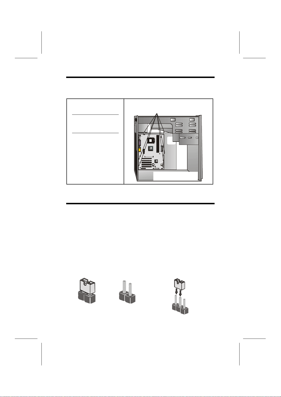
Refer to the following illustration and instructions for installing the mainboard
in a case:
This illustration shows an ex-
ample of a mainboard being
installed in a tower-type case:
Note: Do not overtighten
the screws as this
can stress the main-
board.
Most system cases have
mounting brackets installed in
the case, which correspond to
the holes in the mainboard.
Place the mainboard over the
mounting brackets and secure
the mainboard onto the mount-
ing brackets with screws.
2. Secure the mainboard with
screwswhereappropriate.
1. Place the mainboard
over the mounting brackets.
Ensure that your case has an I/O template that supports the I/O ports and
expansion slots on your mainboard.
C
Ch
he
ec
ck
ki
in
ng
g
J
Ju
um
mp
pe
er
r
S
Se
et
tt
ti
in
ng
gs
s
This section explains how to set jumpers for correct configuration of the main-
board.
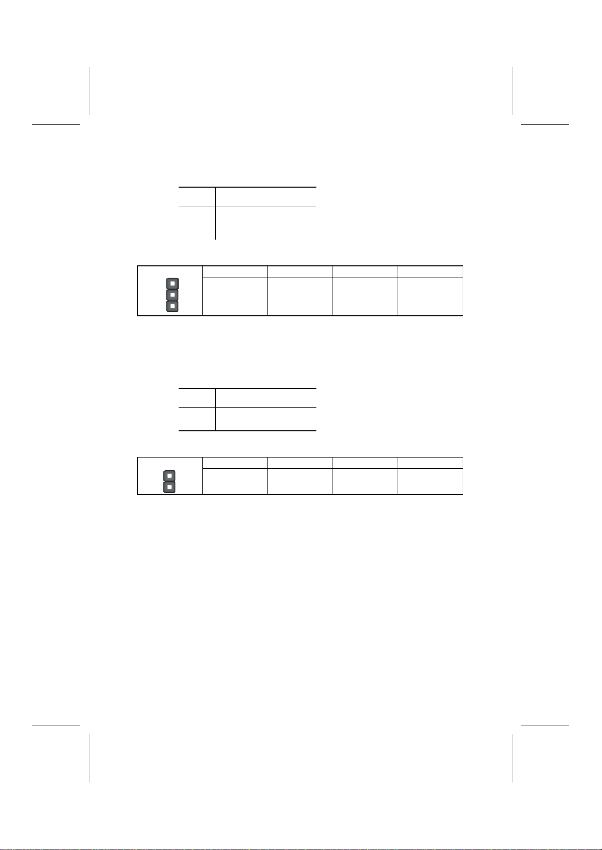
Setting Jumpers
Use the mainboard jumpers to set system configuration options. Jumpers with
more than one pin are numbered. When setting the jumpers, ensure that the
jumper caps are placed on the correct pins.
The illustrations below show a 2-pin jumper.
When the jumper cap is placed on both pins,
the jumper is SHORT. If you remove the
jumper cap, or place the jumper cap on just
one pin, the jumper is OPEN.
This illustration shows a 3-pin
jumper. Pins 1 and 2 are SHORT.
Short Open 123
L7VTA3 V3.1a
9
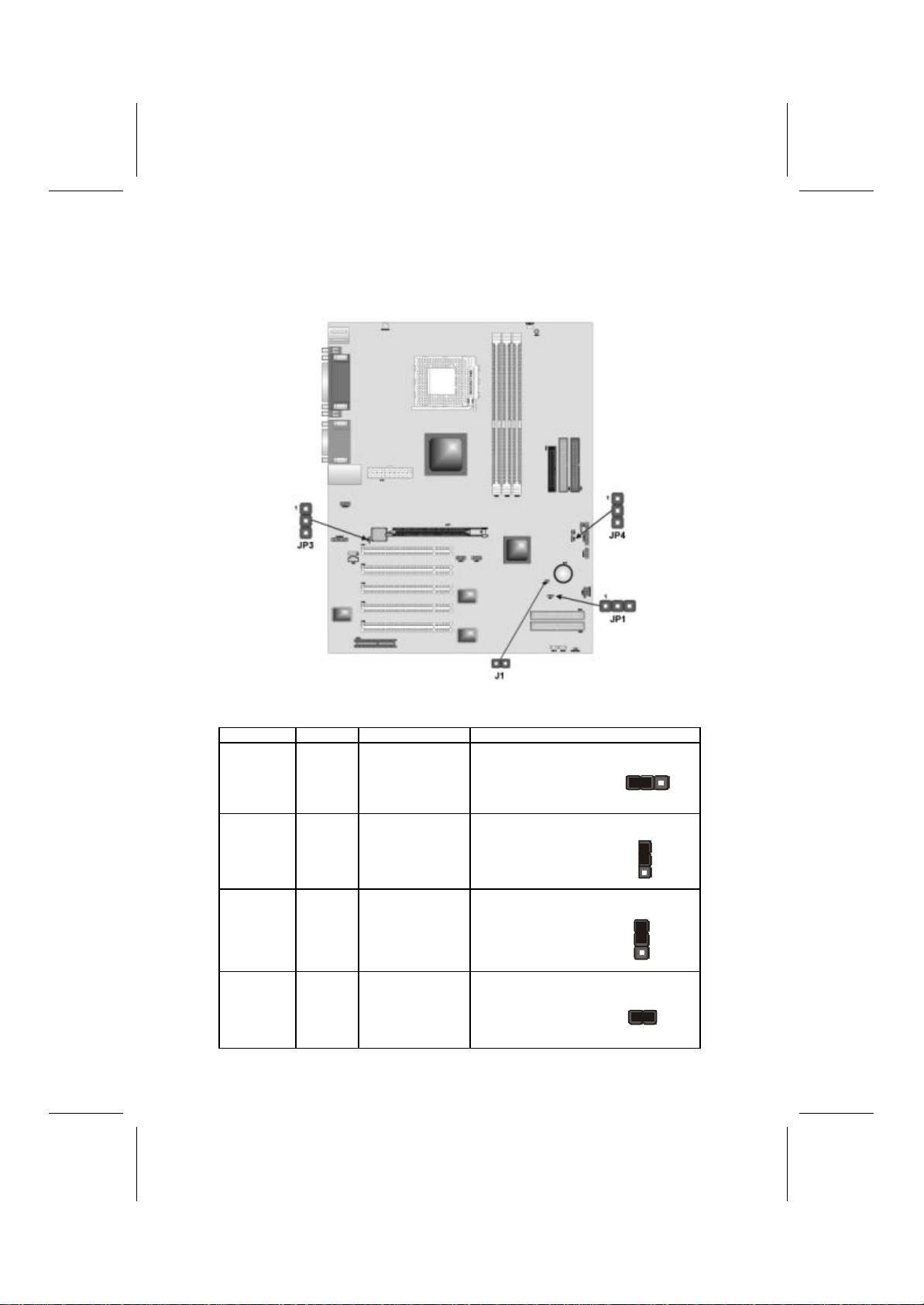
Checking Jumper Settings
The following illustration showsthe location of the mainboard jumpers. Pin 1 is
labeled.
Jumper Settings
Jumper Type Description Setting (default)
JP1 3-pin Clear CMOS 1-2: Normal
2-3: Clear
JP1
1
JP3 3-pin BIOS Protect 1-2: Disable
2-3: Enable
JP3
1
JP4 3-pin CPU frequency
select 1-2: 100 MHz
2-3: 133 MHz
JP4
1
J1 2-pin Chassis detect Short 1-2: Case
Open
Open 1-2: Case
Close
J1

L7VTA3 V3.1a
10
JP1 –Enables you to clear the BIOS. Follow these instructions:
2. Turn the system off.
3. Short pins 2 and 3 on jumper 1.
4. Return the jumper to the normal setting.
5. Turn the system on. The BIOS is returned to the default settings.
JP3 –Enables you to prevent the BIOS from being updated (flashed). Set the
jumper to disabled if you are going to update your BIOS. After updating the
BIOS, return it to the default setting (enabled). For instructions on updating
the BIOS refer to Chapter 3.
JP4 –Use this jumper to select the CPU frequency.
J1 –This connector allows the user to detect unauthorized intrusion to the
case. It will alert the user with a warning message when the case is turned on.
C
Co
on
nn
ne
ec
ct
ti
in
ng
g
C
Ca
as
se
e
C
Co
om
mp
po
on
ne
en
nt
ts
s
After you have installed the mainboard into a case, you can begin connecting
the mainboard components. Refer to the following:
1. Connect the case
power supply
connector to ATX1.
2. Connect the CPU
cooling fan cable to
CPUFAN1.
3. Connect the case
cooling fan connector
to CASFAN1.
4. Connect the case
speaker cable to
SPEAKER1.
5. Connect the case
LED cable to
SJ1/LSJ1 (OEM
customer only).
6. If your case has a
case open alarm
cable, connect it to
J1.
SPEAKER1: Speaker connector
Connect the internal speaker connector to this header.
Pin Signal Name
1
2
3
4
External speaker
NC
NC
VCC
L7VTA3 V3.1a
11
SJ1: Single color LED header
This header allows the user to install an LED indicator to indicate when the
computer is in Suspend to RAM (STR) mode or normal mode.
Pin Signal Name
1
2
3
SUSLED-G
SUSLED-G
5VSB
ACPI LED function:
S0 S1 S3 S4/S5
SJ1
1
Light Blinking Blinking Dark
LSJ1: Single color LED header
This header which is specially designed for OEM customers allows the user to
install a LED indicator to indicate when the computer is in Suspend to RAM
(STR) mode or normal mode.
Pin Signal Name
1
25 VSB
SUSLED-Y
ACPI LED function:
S0 S1 S3 S4/S5
LSJ1
Dark Dark Light Dark
L7VTA3 V3.1a
12
The Panel Connectors
The panel connector (PANEL1 and LPANEL1) provides a standard set of
switch and LED connectors commonly found on ATX or micro-ATX cases.
The LPANEL1 connector is designed specially for OEM customers, which
comply with the OEM specifications. Refer to the table below for information:
PANEL1
Device Pins
N/C 10
Empty 9
Power ON/OFF 6, 8
Reset Switch 5, 7
Green LED
Indicator 2, 4
HDD LED +1, -3
HDD LED
(Pins 1, 3)
2 1
Reset Switch
(Pins 5, 7)
Power Switch
(Pins 6, 8)
Green LED
(Pins 2, 4)
Empty
(Pin 10)
10 9
N/C
(Pin 9)
LPANEL1
Device Pins
Empty 13
Reset Switch +12, -14
Power Switch +9, -11
Speaker +4, -6, -8, 10
Power LED -3 (Y), -5 (G), +7
HDD LED +1, -2
HDD LED
(Pins +1, -2)
2 1
Reset Switch
(Pins +12, -14)
Speaker
(Pins +4, -6,
-8, 10)
Empty
(Pin 13)
14 13
Power Switch
(Pin +9,-11)
Power LED
(Pin -3, -5, +7)
Note:The plus sign (+) indicates a pin which must be connected to a positive
voltage.
L7VTA3 V3.1a
13
I
In
ns
st
ta
al
ll
li
in
ng
g
H
Ha
ar
rd
dw
wa
ar
re
e
Installing the Processor
Caution: When installing a CPU heatsink and cooling fan make sure that
you DO NOT scratch the mainboard or any of the surface-mount resistors
with the clip of the cooling fan. If the clip of the cooling fan scrapes
across the mainboard, you may cause serious damage to the mainboard
or its components.
On most mainboards, there are small surface-mount resistors near the
processor socket, which may be damaged if the cooling fan is carelessly
installed.
Avoid using cooling fans with sharp edges on the fan casing and the
clips. Also, install the cooling fan in a well-lit work area so that you can
clearly see the mainboard and processor socket.
Before installing the Processor
This mainboard automatically determines the CPU clock frequency and sys-
tem bus frequency for the processor. You may be able to change these
settings by making changes to jumpers on the mainboard, or changing the
settings in the system Setup Utility. We strongly recommend that you do not
overclock processors or other components to run faster than their rated speed.
Warning: Overclocking components can adversely affect the reliability of
the system and introduce errors into your system. Overclockingcanper-
manently damage the mainboard by generating excess heat in
components that are run beyond the rated limits.
This mainboard has a Socket 462 processor socket. When choosing a proc-
essor, consider the performance requirements of the system. Performance is
based on the processor design, the clock speed and system bus frequency of
the processor, and the quantity of internal cache memory and external cache
memory.
L7VTA3 V3.1a
14
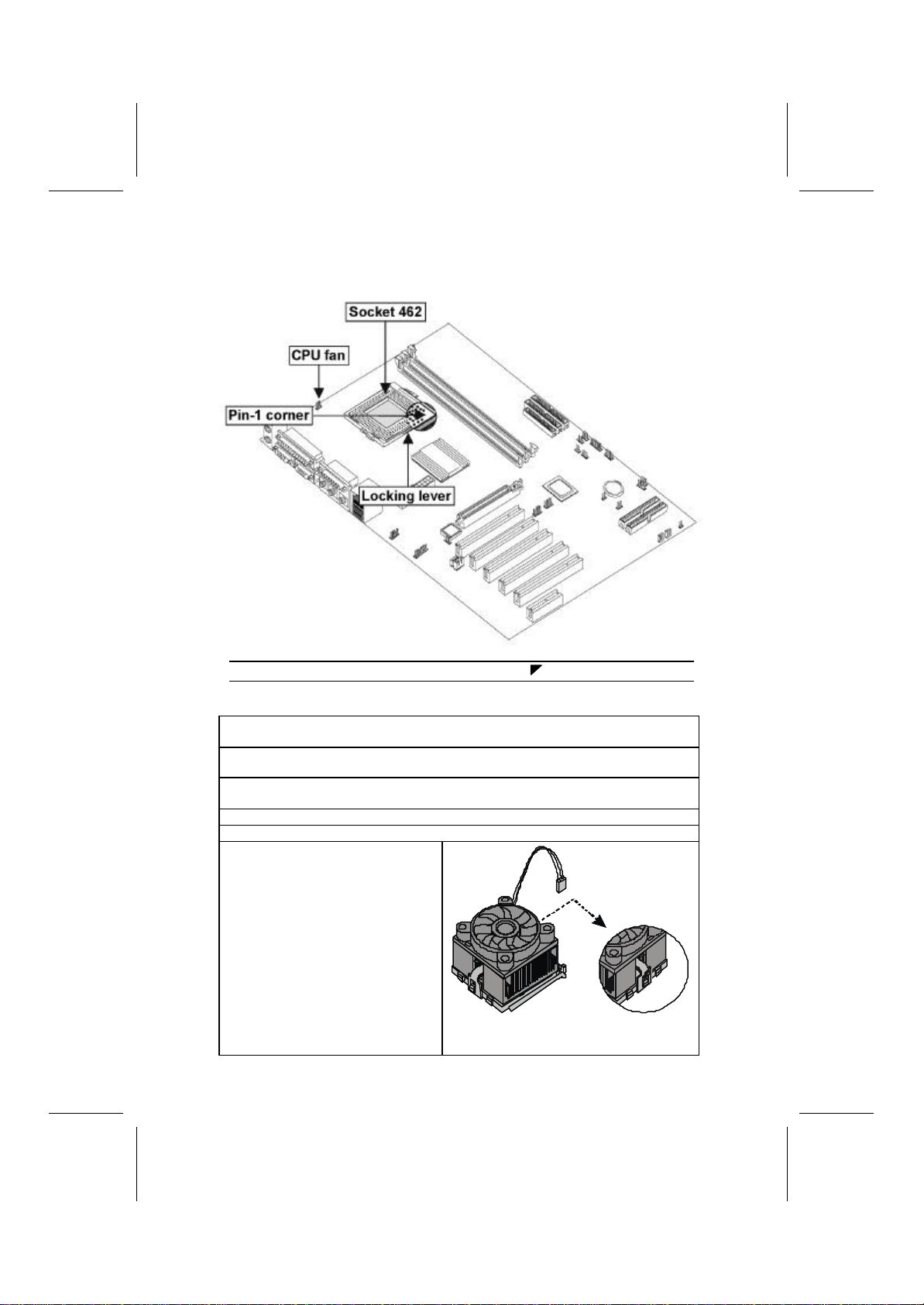
CPU Installation Procedure
The following illustration shows CPU installation components:
Note: The pin-1 corner is marked with an arrow
Follow these instructions to install the CPU:
1. Pull the CPU socket locking lever away from the socket to unhook it and raise
the locking lever to the upright position.
2. Identify the pin A-1 corner on the CPU socket and the pin A-1 corner on the
processor.
3. Swing the locking lever down and hook it under the latch on the edge of the
socket.
4. Apply thermal grease to the top of the CPU.
5. Lower the CPU cooling fan/heatsink assembly onto the CPU.
6. Secure the two retention clips
on either side of the
fan/heatsink unit onto the socket
base.
Fan/heatsink unit
secured to socket

L7VTA3 V3.1a
15
7. Connect the CPU Cooling Fan
power cable connector to the
CPUFAN connector.
Notes:
1. CPU fan and heatsink installation procedures may vary with the type of
CPUfan/heatsink supplied. The form and size of fan/heatsink may also vary.
2. After you have assembled the system, you must set the correct clock speed
and frontside bus (FSB) speed. Check the jumper section and refer toChap-
ter 3 “Frequency Voltage Control” for more information.
L7VTA3 V3.1a
16
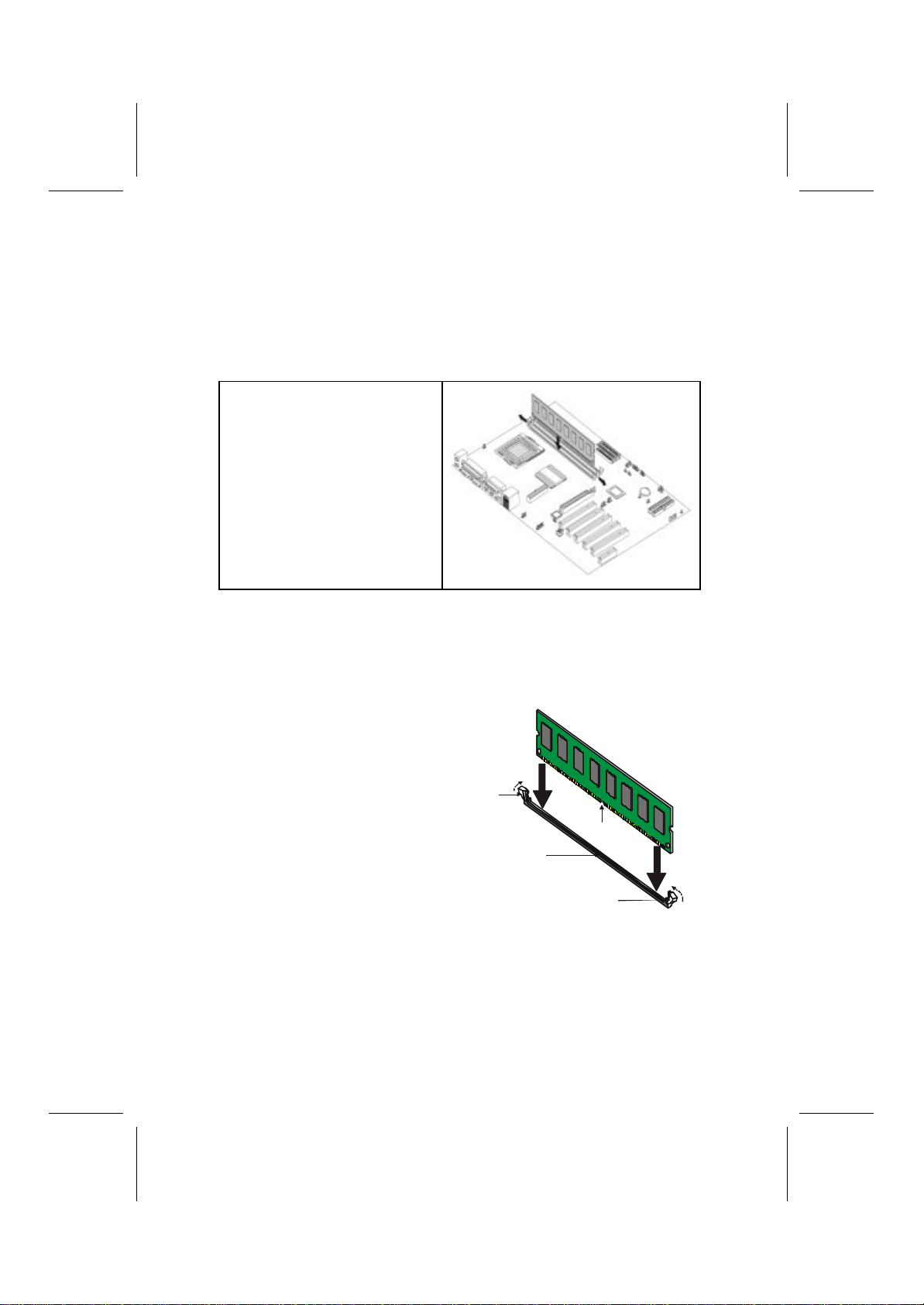
Installing Memory Modules
This mainboard accommodates 184-pin 2.5V unbuffered Double Data Rate
(DDR) SDRAM memory modules. The memory chips must be standard or
registered SDRAM (Synchronous Dynamic Random Access Memory). The
memory bus runs at 100/133/166 MHz.
Installation Procedure
The mainboard accommodates three
memory modules. You must install at
least one module in any of the three
slots. Each module can be installed
with 32 MB to 512 MB of memory;
total memory capacity is 1.5 GB.
Refer to the following to install the memory modules.
1. Push the latches on each side of the DIMM slot down.
2. Align the memory module with the slot. The DIMM slots are keyed with
notches and the DIMMs are keyedwith cutouts so that they can only be
installed correctly.
3. Check that the cutouts on the
DIMM module edge connector
match the notches in the
DIMM slot:
4. Install the DIMM module into
the slot and press it firmly
down until it seats correctly.
The slot latches are levered
upwards and latch on to the
edges of the DIMM.
5. Install any remaining DIMM
modules.
Cutout
Notch
Latch
Latch
Table of contents
Other ECS Motherboard manuals


 manual")


