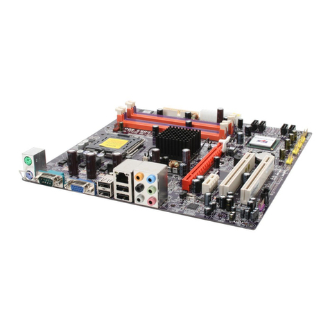
ECS P5HX-A User manual

P5HX-A
User’s Manual 3-1
1 Introduction
Mainboard Description
Processor Expansion Slots
Chipset PS/2 Mouse & Keyboard Set
System BIOS Serial / Parallel Ports
L2 On-board Cache PCI IDE Connectors
L2 Cache Module FDD Connector
SIMM System Memory
Socket Power Supply Connectors

P5HX-A
User’s Manual 3-2
P5HX-A is a new generation ATX form factor Pentium PCI mainboard using Intel
430HX PCIset (TXC, PIIX 3) and SMC 37C669 I/O Chip. It delivers great
performance with industry standard EDO memory and PB SRAM cache with
concurrent PCI 2.1, APM, Plug & Play, PCI Bus Master IDE, and parity /
ECC……etc. P5HX-A is designed to run rich business applications.
1. Processor:
Intel Pentium75/90/100/120/133/150/166/200 MHz
Intel Pentium with MMX technology (P55C)
Cyrix 6x86 P120+/P133+/P150+/P166+
Cyrix 6x86 L
2. Chipset:
Intel 430HX 82439HX (TXC) / 82371AB (PIIX3)
SMC 37C669 (SUPER I/O)
3. System BIOS:
Award BIOS
4. L2 On-board Cache:
Provide Pipleined Burst SRAM 256/512 KB
On-board cache 256KB / 512KB
5. L2 Cache Module :
An optional ECS M161”or later version of upgrade cache module can be
inserted to expand the cache memory size to 256KB or 512KB.
An OASt 2.0”or later cache module can also be used to upgrade the cache
memory size.
6. SIMM System Memory Socket:
Support 72-pin SIMMs of 4MB, 8MB, 16MB ,32MB or 64MB to form a
memory size between 8MB to 256MB
7. Expansion Slot:
4 ISA Bus Slots.
4 PCI Bus Slots. (One ISA-PCI Shared Slot)
8. PS/2 Mouse & Keyboard Set:
Provide Connectors for PS/2 Keyboards & PS/2 Mouse.
9. Serial / Parallel Port:
Provide two serial port connectors and one parallel port connector.
10. PCI IDE Connector:
2 Enhanced PCI IDE up to 4 IDE Device Connectors.
11. FDD Connector:
Provide an on-board FDD Connector which supports
360KB/720KB/1.2MB/1.44MB/2.88MB type drives.
12. Power Supply Connectors:

P5HX-A
User’s Manual 3-3
Provide the connectors for standard PC power supply or ATX power supply.

P5HX-A
User’s Manual 3-4
Features
qCPU:
•One Socket 7 supports Pentium 75/90/100/120/133/150/166/200 MHz
CPU and Intel Pentium OverDrive CPUs.
•Manufacture optional 2nd Regulator to support Intel Pentium with MMX
technology.(P55C)
•Support Cyrix P120+/P133+/P150+/P166+ CPU.
•Support Cyrix 6x86 L.
qBIOS:
•Support Award BIOS with flash ROM.
ÄPNP specification V1.0a
ÄAPM specification V1.2
ÄDMI specification
ÄBoot from CD-ROM
qCache:
•Support the CPU internal first level (L1) cache and external
secondary level (L2) cache.
>16KB Level 1 Cache: (Pentium)
ÄData Cache: support 8KB Write-Through and Write-Back policy.
ÄCode Cache: support 8KB Write-Through policy.
>256KB /512KB (optional) Pipelined Burst SRAM On
Board.
>160-pin Cache Module Socket for Level 2:
ÄSupport COASt 2.0 or later Pipelined Burst for 256KB or 512KB.
ÄAn optional ECS “CM161 “or later version of upgrade cache
module can be inserted to expand the cache memory size to
256KB or 512KB.
qMemory:
•Support 4 pieces of 72-pin SIMM sockets with memory size from 8MB to
256MB.

P5HX-A
User’s Manual 3-5
•Support EDO/ Fast Page Mode DRAM.
•Support parity check or ECC function with parity SIMMs.
qSlots:
•Four 16-bit ISA slots with 100% ISA compatible function.
•Four 32-bit PCI slots support PCI Bus master.
ÄPCI specification version 2.1.
ÄCPU to PCI memory write posting with 4 word deep buffers.
ÄConverts Back-to-Back sequential CPU to PCI memory writes to PCI
Burst writes.
qFDD:
•Two floppy support 360KB, 720KB, 1.2MB, 1.44MB, 2.88MB, and 3
Mode floppy drives.
qRTC:
•Use Dallas 12B887 compatible RTC module (Internal 128 byte of CMOS
RAM).
qIDE:
•Build-in Intel 430HX PCIset chip 32-bit PCI IDE interface with 2 IDE
channels.
•Support PIO mode 4 or DMA mode 2 with transfer rate up to 22MB/sec.
qPower Management:
Use ATX power supply to support software power down function which is
following APM V1.2.Memory Configurations
This chapter contains the detailed memory configuration: System Memory and
Cache Memory.

P5HX-A
User’s Manual 3-6
The diagram above displays the location of SIMM Sockets, Pipelined Burst SRAM
and L2 Cache module on P5HX-A motherboard.
Cache Memory
System Memory

P5HX-A
User’s Manual 3-7
System Memory
The following table lists a number of possible DRAM combinations.
Bank 0 Bank 1 Total
SIMM1 SIMM2 SIMM3 SIMM4 Memory Size
4MB 4MB ----- ----- 8MB
8MB 8MB ----- ----- 16MB
16MB 16MB ----- ----- 32MB
32MB 32MB ----- ----- 64MB
64MB 64MB ----- ----- 128MB
4MB 4MB 4MB 4MB 16MB
4MB 4MB 8MB 8MB 24MB
4MB 4MB 16MB 16MB 40MB
4MB 4MB 32MB 32MB 72MB
4MB 4MB 64MB 64MB 136MB
8MB 8MB 8MB 8MB 32MB
8MB 8MB 16MB 16MB 48MB
8MB 8MB 32MB 32MB 80MB
8MB 8MB 64MB
P
64MB
P
144MB
Continued.....
SIMM:
P5HX-A provides tremendous flexibility DRAM configurations.
It accepts a maximum of 256MB memory size. The on-board
DRAM is installed with SIMM (Single-In-line-Memory Module).
There are two memory banks which support the
4M/8M/16M/32M/64M type, single and/or double-density
modules. The DRAM type of SIMM1 /SIMM2 is independent of
SIMM3/SIMM4.
The type of SIMM1 and SIMM2 must be same if they
exist at the same time.

P5HX-A
User’s Manual 3-8
Bank 0 Bank 1 Total
SIMM1 SIMM2 SIMM3 SIMM4 Memory Size
16MB 16MB 16MB 16MB 64MB
16MB 16MB 32MB 32MB 96MB
16MB 16MB 64MB
P
64MB
P
160MB
32MB 32MB 32MB 32MB 128MB
32MB 32MB 64MB
P
64MB
P
192MB
64MB
P
64MB
P
64MB
P
64MB
P
256MB
Table 1 -1. System Memory Configurations
P
: means the memory size is not available for testing now.
Cache Memory Subsystem
Level 1 Cache
16 KB Level 1 Cache that builds in Pentium CPU includes Data Cache and Code
Cache.
•1. Data Cache: supports 8KB Write-Through and Write-Back policy.
•2. Code Cache: supports 8KB Write-Through policy.
Level 2 Cache
L2 Cache On-board Cache Module Total Memory Size
0 KB 256KB 256KB
0 KB 512KB 512KB
256KB 256KB 512KB
512KB 0KB 512KB
1. If there is an n-board 256KB L2 Cache”in the motherboard, users may
either upgrade to 512KB by inserting an ECS M161”or COASt (2.0 or
later) upgrade cache module of 256KB.
2. If there is not any n-board 256KB L2 Cache”in the motherboard, users
may either upgrade to 256KB or 512KB by inserting an ECS M161”or
COASt (2.0 or later) upgrade cache module of 256KB or 512KB.

P5HX-A
User’s Manual 3-9
2 Jumpers and Connectors
Setting the Jumpers
Set bus frequency and CPU frequency
Core CPU
Freq. (MHz) Host
Clock (MHz) JP9 Clock
Multiplier JP7
P
JP8
75 50 short 1-2, 3-4 1.5 short 1-2 short 1-2
90 60 short 3-4 1.5 short 1-2 short 1-2
100 66 short 1-2 1.5 short 1-2 short 1-2
110 55 open 2short 1-2 short 2-3
120 60 short 3-4 2short 1-2 short 2-3
133 66 short 1-2 2short 1-2 short 2-3
150 60 short 3-4 2.5 short 2-3 short 2-3
166 66 short 1-2 2.5 short 2-3 short 2-3
200 66 short 1-2 3short 2-3 short 1-2
Table 2 -1. Host Clock, CPU type and Speed Settings
P: Cyrix 6x86 CPU does not have multiplier 1.5 and 2.5 . Leave JP7 open for
Cyrix 6x86 CPU.
Cyrix 6x86 CPU and AMD K5 CPU use P-rating as the CPU frequency.
Refer the following table to get the CPU core frequency. For AMD K5 CPU,
check your CPU vendor for detailed information.
Cyrix 6x86 Core CPU Frequency (MHz)
P120+ 100
P133+ 110
P150+ 120
P166+ 133
Set CPU Voltage Type
Single JP2, JP3 CPU Voltage JP1

P5HX-A
User’s Manual 3-10
Voltage CPU JP4, JP5
short 1-2
short 1-2
3.3V (STD)
(default) short 1-2
short 1-2
short 1-2 3.52V (VRE) short 3-4
Dual
Voltage CPU
JP2, JP3
JP4, JP5 CPU I/O
Voltage JP1 CPU core
Voltage JP17
P
(Split Power
Plane CPU) short 2-3
short 2-3 3.3V (STD) short 1-2 2.5V short 1-2
short 2-3
short 2-3 2.7V short 3-4
2.8V short 5-6
2.9V short 7-8
3.52V (VRE) short 3-4 2.5V short 1-2
2.7V short 3-4
2.8V short 5-6
2.9V short 7-8
Table 2 -2CPU Voltage Settings
P: If you have split power plane CPU ( There are different Voltage between
CPU Core and I/O ), Please check CPU vendor or us in order to decide
core voltage value of JP17.
Check your processor documentation for correct voltage setting to avoid
the damage of CPU.
Single Voltage CPU : Intel Pentium and OverDrive series, Cyrix 6x86,
AMD K5.
Dual Voltage CPU: Intel Pentium with MMX technology (P55C),
Cyrix 6x86 L, M2 dual voltage, AMD K5 dual voltage CPU.
Set Cache Memory Size
256KB
(256KB Cache Module only) JP15 open
256KB
(On-board 32Kx32 Burst SRAM only) JP15 short
512KB
(512KB Cache Module only) JP15 open

P5HX-A
User’s Manual 3-11
512KB
(on-board 256KB 32Kx32 Burst SRAM
and 256KB Cache Module)
JP15 short
512KB
(on-board 512KB 64Kx32 Burst SRAM
only)
JP15 open
Table 2 -3Cache Memory Size Settings
Set CMOS RAM Clear Switch
BIOS Setting values and password are stored in CMOS RAM. To clear CMOS
Data, please open your computer chassis; short JP11; power on your system
carefully ; power off your system ; close your computer chassis; and then CMOS
data will be cleared.
Normal (default) JP11 short 2-3
CMOS Data Clear JP11 short 1-2
Table 2 -4. CMOS RAM Clear Settings
Set Password Check Switch
Enabled or disable BIOS password check.
Password Password Check Disabled JP18 short 1-2
Check Switch Password Check Enabled JP18 short 2-3
Table 2 -5. Password Check Settings

P5HX-A
User’s Manual 3-12
Green Function
CPU Cooling Fan Control
P5HX-A provides the ability to turn the CPU cooling fan off while the system is in
low-power suspend mode. Please connect the CPU cooling fan to J18 and enable
PU Fan Power Green”function in BIOS ower Management Setup “in
order to make it work.
Green Function Indicator
Connect the LED to J8. The LED blinking indicates the system in low-power
suspend mode.
1 2
J8
+
-
Graphic Descriptions of Jumper Settings
means Pin 1 & 2 are set as
“s
hort”
means this jumper is set as
“o
pen”
1
1

P5HX-A
User’s Manual 3-13
CPU Type (The jumpers block for most used CPU)
1. Intel Pentium 75MHz CPU
(50MHz Host Clock) installed
on board
2. Intel Pentium 90MHz CPU
(60MHz Host Clock) installed
on board
3. Intel Pentium 100MHz CPU
(66MHz Host Clock) installed
on board
4. Intel Pentium 120MHz CPU
(60MHz Host Clock) installed
on board

P5HX-A
User’s Manual 3-14
5. Intel Pentium 133MHz CPU
(66MHz Host Clock) installed
on board
6. Intel Pentium 150MHz CPU
(60MHz Host Clock) installed
on board
7. Intel Pentium 166MHz CPU
(66MHz Host Clock) installed
on board
8. Intel Pentium 200MHz CPU
(66MHz Host Clock) installed
on board
9. Intel P55C 166MHz CPU
(66MHz Host Clock) installed
on board

P5HX-A
User’s Manual 3-15
10. Intel P55C 200MHz CPU
(66MHz Host Clock) installed
on board
11. Cyrix 6X86 100MHz CPU
(50MHz Host Clock) installed
on board
12. Cyrix 6X86 110MHz CPU
(55MHz Host Clock) installed
on board
13. Cyrix 6X86 120MHz CPU
(60MHz Host Clock) installed
on board

P5HX-A
User’s Manual 3-16
14. Cyrix 6X86 133MHz CPU
(66MHz Host Clock) installed
on board
CPU Voltage Selection

P5HX-A
User’s Manual 1-17

P5HX-A
User’s Manual 1-18
Connectors
The following table lists the connectors located on the P5HX-A. They can be used
to connect with some peripheral devices to enhance the operating performance of
the system. Please refer to the mainboard layout figure on the next page for their
positions.
Connector Function
J1 PS/2 Keyboard Connector
J3 PS/2 Mouse Connector
J4 COM1 Port
J5 COM2 Port
J6 Parallel Port
J8 Green Function Indicator
J9 FDD Connector
J10 Primary IDE Connector
J11 Secondary IDE Connector
J12
J13 HDD LED
J16 Cache Module
J17 USB 1/2 Header (Optional)
Pin 1, 6 : VCC Pin 2 , 7 : DATA - Pin 3 , 8 : DATA +
Pin 4 , 5, 9 , 10 : GND
1
2
3
4
5
6
7
8
9
10
Continued.....

P5HX-A
User’s Manual 1-19
Connector Function
J18 CPU Fan Power
+12V
1 23
GND
J19 Fast IR Header (Optional)
1
2
34 567
IRRX GND IRR3 GND
GND VCC VCC
J20 IR Header (Intel)
1
2
34 5
VCC IRRX IRTX
NC GND
J21 ATX Power ON/OFF Switch
PS1 AT Power Supply Connector
PS2 ATX Power Supply Connector
Table 2 -6. Connectors

P5HX-A
User’s Manual 1-20
Board Layout
Figure 2 -1. P5HX-A Mainboard Layout
Table of contents
Other ECS Motherboard manuals
Popular Motherboard manuals by other brands
Intel
Intel DG31PR - Desktop Board Classic Series... Specification update
ASROCK
ASROCK 970 Pro2 Quick installation guide
Freescale Semiconductor
Freescale Semiconductor KIT22XS4200EKEVB manual
Asus
Asus M2R-FVM owner's manual
Nuvoton
Nuvoton NuMicro NuTiny-SDK-NUC505 user manual

JETWAY
JETWAY 830CN user manual

American Megatrends
American Megatrends MegaRUM user guide
IEI Technology
IEI Technology IMBA-X9654 Quick installation guide
VIA Technologies
VIA Technologies EPIA-P900 user manual
GIGA-BYTE TECHNOLOGY
GIGA-BYTE TECHNOLOGY MDH11BM user manual
Biostar
Biostar TA890FXE - BIOS manual
ASROCK
ASROCK P4I945GC - V1.0 user manual
