EG&G ORTEC 260 User manual
too
MIDLAND
ROAD.
OAK
RIDGE
TENNESSEE,
37830
AREA
CODE
(615)
483-8451
TWX
810-572-1078
INSTRUCTION
MANUAL
260
TIME
PICKOFF
UNIT
AN
COMPANY
INSTRUCTION
MANUAL
260
TIME
PICKOFF
UNIT
S^al
No.
Purchaser
Date
Issued
ORTEC
INCORPORATED
P.
0.
BOX
0
OAK
RIDGE,
TENNESSEE
37830
Telephone
(615)
483-8451
TWX
810-572-1078
@
ORTEC
Incorporated
1966
Printed
In
U«S«Aa
TABLE
OF
CONTENTS
Page
WARRANTY
PHOTOGRAPH
1.
DESCRIPTION
1-1
2.
SPECIFICATIONS
2-1
3.
INSTALLATION
INSTRUCTIONS
3-1
4.
OPERATING
INSTRUCTIONS
4-1
4.1
Initial
Checkout
and
Familiarization
4-
1
4.2
Application
Notes
4-
1
5.
CIRCUIT
DESCRIPTION
5-1
6.
MAINTENANCE
INSTRUCTIONS
6-1
6.1
Testing
Performance
6-
1
6.2
Calibration
Adjustments
6-
1
6.3
Suggestions
for
Troubleshooting
6-
1
SCHEMATIC
ORTEC
260
Time
Pickoff
260-Sl

LIST
OF
FIGURES
AND
ILLUSTRATIONS
Page
Figure
2-1.
Plof
of
ORTEC
260
Threshold
SensiH
vify
vs
Det-ector
Capacity
2-2
Figure
2-2.
Typical
Block
Diagram
for
Timing
With
Semiconductor
Detectors
2-3
Figure
4-1.
Pileup
Reduction
With
260
and
404
4
-2
Figure
4-2.
A
Method
of
Pulse
Shape
Discrimination
4-3
Figure
4-3.
Charged-Porticle
Identification
by
Time-of-Flight
4-4
Figure
4-4.
Beam
Pulse
Time
Pickoff
System
(T
=
O)
for
Pulsed
Accelerators
4-5

A
NEW
STANDARD
TWO-YEAR
WARRANTY
FOR
ORTEC
ELECTRONIC
INSTRUMENTS
ORTEC
warrants
its
nuclear
instrument
products
to
be
free
from
defects
in
workmanship
and
materials,
other
than
vacuum
tubes
and
semiconductors,
for
a
period
of
twenty-four
months
from
date
of
shipment,
provided
that
the
equipment
has
been
used
in
a
proper
manner
and
not
subjected
to
abuse.
Repairs
or
replacement,
at
ORTEC
option,
will
be
made
without
charge
at
the
ORTEC
factory.
Shipping
expense
will
be
to
the
account
of
the
customer
except
in
cases
of
defects
discovered
upon
initial
operation.
Warranties
of
vacuum
tubes
and
semiconductors,
as
made
by
their
manufacturers,
will
be
extended
to
our
customers
only
to
the
extent
of
the
manufacturers'
liability
to
ORTEC.
Specially
selected
vacuum
tubes
or
semiconductors
cannot
be
warranted.
ORTEC
reserves
the
right
to
modify
the
design
of
its
products
without
incurring
responsibility
for
modification
of
previously
manufactured
units.
Since
installation
conditions
are
beyond
our
control,
ORTEC
does
not
assume
any
risks
or
liabilities
associated
with
methods
of
installation
other
than
specified
in
the
instructions,
or
installation
results.
QUALITY
CONTROL
Before
being
approved
for
shipment,
each
ORTEC
instrument
must
pass
a
stringent
set
of
quality
control
tests
designed
to
expose
any
flaws
in
materials
or
workmanship.
Permanent
records
of
these
tests
are
maintained
for
use
in
warranty
repair
and
as
a
source
of
statistical
information
for
design
improvements.
REPAIR
SERVICE
ORTEC
instruments
not
in
warranty
may
be
returned
to
the
factory
for
repairs
or
checkout
at
modest
expense
to
the
customer.
Standard
procedure
requires
that
returned
instruments
pass
the
same
quality
control
tests
as
those
used
for
new
production
instruments.
Please
contact
the
factory
for
instructions
before
shipping
equipment.
DAMAGE
IN
TRANSIT
Shipments
should
be
examined
immediately
upon
receipt
for
evidence
of
external
or
concealed
damage.
The
carrier
making
delivery
should
be
notified
immediately
of
any
such
damage,
since
the
carrier
is
normally
liable
for
damage
in
shipment.
Packing
materials,
waybills,
and
other
such
documentation
should
be
preserved
in
order
to
establish
claims.
After
such
notification
to
the
carrier,
please
notify
ORTEC
of
the
circumstances
so
that
we
may
assist
in
damage
claims
and
in
providing
replacement
equipment
if
necessary.
'I
'
4".'
TIME
PICKOFF
UNIT
[--
>
I—DETfcCTOR
PRbAMP
MODEL
260
I
I
I
II
I

1
-1
}
INSTRUCTION
MANUAL
ORTEC
260
TIME
PICKOFF
UNIT
1.
DESCRIPTION
The
ORTEC
260
Time
Pickoff
Unit-
is
designed
to
obtain
a
timing
signal
directly
from
a
semiconductor
detector
without
significantly
altering
the
energy
resolution
qualities
of
the
detector-linear-amplifier
system.
It
consists
of
a
pulse
transformer,
a
wide-band
transistor
amplifier,
a
tunnel
diode
discriminator,
and
a
line
driver
buffer.
The
unit
is
connected
in
series
between
a
detector
and
a
charge-sensitive
preamplifier;
i.e.,
the
pulse
current
from
the
detector
flows
through
the
primary
of
the
pulse
transformer
en
route
to
the
preamplifier.
The
260
derives
its
power
and
discriminator
control
bias
from
a
remote
location
via
a
shielded
multiconductor
cable.
The
necessary
power
and
control
bias
are
provided
by
a
403A
Time
Pickoff
Control
.
All
signal
input
and
output
connections
are
of
a
BNC
type.
The
260
may
be
used
in
conjunction
with
photomultipliers
to
obtain
timing
signals
frpm
either
the
anode
or
dynode
simply
by
reversing
the
order
of
connections
to
the
transformer
primary.
This
unit
provides
the
necessary
functions
of
amplification
and
low
amplitude
triggering
required
for
signal
leading
edge
time
measurements
with
low
gain
(10-stage)
photomultipliers.
(Refer
to
section
4.2(2).)
The
260
may
also
be
used
in
conjunction
with
electrostatic-inductive
pickup
to
derive
a
timing
pulse
corresponding
to
T
=
0
for
pulsed
accelerators.
(Refer
to
section
4.2
(4).)
The
physical
dimensions
of
the
unit
are
6
x
4
x
1.7
(4.45
x
10.2
x
15.30cm).
I
(
*

2
-
1
I
2.
SPECIFICATIONS
2.1
Input
Polarily-
2.2
Input
Signal
Amplitude-
2.3
Sensitivity
2.4
Time
Pickoff
Effect
on
Energy
Resolution
■Either
positive
or
negative
by
reversing
the
order
of
connections
to
the
input
transformer
primary.
Connect
negative
input
to
BNC
(CN-1)
labeled
DET.,
and
posi
tive
input
to
BNC
(CN-2)
labeled
PREAMP.
-Dependent
on
input
impedance
of
ORTEC
260
amplifier,
which
may
be
changed
by
simple
plug-in
of
a
resistor.
Signal
input
to
the
amplifier
should
not
exceed
2V|
i.e.,
I2
Rj
^2V,
1^
=
1
.5
I2;
therefore,
I]
(max)
^.5/Rj.
I]
and
I2
refer
to
the
primary
and
secondary
pulse
transformer
currents.
-See
figure
1.
-Refer
to
table
1.
2.5
Energy
Variation
Effect
on
Time
Resolution
2.6
Threshold
Range-
2.7
Output
2.8
Power
Requirements-
2.9
Signal
Connections
2.10
Transformer
Insulation—
-Refer
to
table
2.
-s
15.1
-Negative
500
mV
(voltage
drive,
Zq~5
ohms),
Tj.
^
1.2
nsec.
Pulse
width
~10
nsec
(variable)
-+
12V
at
40
mA
or
-
12V
at
40
mA,
plus
discriminator
bios
current.
All
power
is
provided
by
a
Time
Pickoff
Control
Unit
(ORTEC
403A)
via
a
multiconductor
shielded
cable.
-BNC
type
-1
kV
Table
1.
Time
Pickoff
Effect
on
Energy
Resolution
(RC
Mode)
(Typical
Measurement)
Detector
Pulser
Width
Pulser
Width
Capacity
Without
Time
Pickoff
With
Time
Pickoff
(pF)
(keV)
(keV)
0
5.9
7.3
20
6.05
7.8
50
7.35
8.9
100
8.85
11.0
200
12.1
14.7
Note:
The
detector
capacity
indicated
is
in
addition
to
approximately
25
pF
cable
capacity.

2-2
I
Table
2.
Signal
Energy
Effect
on
Pickoff
Output
Time
(Typical
Measurement)
Signal
Amplitude
Time
Shift
Jitter
(FWHM)
(MeV,
Si
Detector)
(nsec)
(psec)
0.25
(Threshold)
0
150
0.5
1.2
86
1.25
1.9
73
2.5
2.5
68
5.0
2.7
62
Note:
The
pulse
generator
used
is
a
mercury-switch,
delay-line
type
(T^
<0.3
nsec).
600
LU
-J
3
O-
s
CM
U
UJ
H-
o
>
<D
>-
o
CSC
LU
z
LU
Q
_J
o
X
OO
LU
CC
X
400
200
c
)
.
ORTEC
*0017
0
100
200
500
SIMULATED
DETECTOR
CAPACITY
Figure
2-1
Plot
of
ORTEC
260
Threshold
Sensitivity
vs
Detector
Capacity

2-3
2-0=
son
I
1
CHARGE
TERMINATOR
CHARGE-SENSITIVE
PREAMPLIFIER
LINEAR
AMPLIFIER
DETECTOR
I
ANALYZER,
ETC,
PARTICLE
BEAM
PREAMP
DET.
POWER
a
CONTROL
BIAS
ORTEC
200172
OUTPUT
>—a
PRECISION
PULSE
GEN
FA^OUJ_^F^^R
7
outputs}
INPUT
A
403A
TIMING
SIGNALS
Figure
2-2
Typical
Block
Diagram
for
Timing
Wifh
Semiconductor
Detectors

3
-
1
3.
INSTALLATION
INSTRUCTIONS
3.1
CAUTION:
Before
applying
a
pulser
or
connecHng
to
a
photomultiplier,
refer
to
section
2.2.
3.2
Connect
the
260
between
the
detector
and
charge-sensitive
preamplifier
input
as
indicated
by
the
arrows
at
the
two
input
BNC
connectors.
The
inputs
are
indicated
for
electron
signal
collection.
(See
block
diagram,
figure
2.)
3.3
Connect
a
precision
pulse
generator
via
a
charge
terminator
in
parallel
with
the
de
tector
as
shown
in
the
block
diagram
(figure
2).
3.4
Connect
the
power
coble
between
260
and
403A
Time
Pickoff
Control
Unit.
3.5
Connect
50-ohm
coaxial
cable
from
260
output
to
input
of
fanout
buffer
of
Time
Pickoff
Control,
to
scope
input,
or
to
other
time
monitoring
point.
The
coaxial
cable
should
be
terminated
at
the
receiving
end.
3.6
Control
of
the
260
Time
Pickoff
is
now
handled
completely
by
the
403A
Time
Pickoff
Control
Unit.
3.7
Set
the
Control
Unit
discriminator
level
(R9)
at
1000.
3.8
Turn
on
Control
Unit
power.
3.9
The
discriminator
level
may
now
be
adjusted
to
the
energy
level
desired.
The
dis
criminator
should
trigger
on
amplifier
noise
when
the
level
is
set
very
near
zero.

4-
1
4.
OPERATING
INSTRUCTIONS
4.1
Initial
Checkout
and
Familiarization
(1)
Connect
the
unit
as
described
in
the
installation
instructions
(section
3).
(The
detector
need
not
be
connected
for
checkout.)
In
some
applications,
it
may
be
desirable
to
replace
the
charge-sensitive
preamplifier
by
a
fixed-capacity,
delay-line
terminating
impedance,
or
short-circuit
terminator.
Use
a
pulser
such
as
the
ORTEC
204
or
419
Precision
Pulse
Generator
or
any
mercury
switch
delay-
line
pulser
with
a
rise
time
of
less
than
2
nanoseconds.
If
a
delay-line
pulser
is
used,
set
the
pulse
width
to
2-10
nanoseconds,
and
use
a
terminating
impedance
in
place
of
the
charge-sensitive
preamplifier.
(2)
Adjust
the
pulser
amplitude
to
the
equivalent
of
~10
mV
into
100
ohms
before
connecting
to
the
260.
(Refer
to
section
2.2.)
(3)
Connect
pulser,
turn
on
power
to
Time
Pickoff
Control,
and
adjust
the
discriminator
level
to
obtain
an
output
pulse.
If
a
precision
pulse
generator
is
used,
it
may
be
calibrated
in
energy
and
then
the
pulser
becomes
an
energy
reference
to
both
the
energy
analysis
system
and
the
discriminator
of
the
260.
4.2
Application
Notes
Refer
to
the
next
four
pages
for
four
different
applications
using
this
equipment.

4-2
APPLICATION
NOTES
(1)
Inspecfion
and
Pileup
Reduction
Figure
3
is
a
block
diogrom
of
the
experimental
setup
for
removing
from
a
spectrum
those
pulses
which
have
the
wrong
amplitude
because
of
multiple
pulses
arriving
in
a
detector
within
a
period
of
time
corresponding
to
the
linear
amplifier
resolving
time.
This
is
especial
ly
important
when
pulse
height
analysis
is
performed
on
a
complicated
spectrum
containing
many
pulse
amplitudes
and
widely
varying
relative
rates.
Inspection
by
this
method
reduces
the
relative
pileup
time
from
3.3
microseconds
for
a
double-del
ay-line
clipped
amplifier
with
1-microsecond
clipping
lines
to
approximately
250
nanoseconds.
This
is
a
reduction
factor
of
approximately
12
in
the
number
of
counts
in
any
random
sum
or
difference
peak.
DETECTOR
I'
-OAOltr
CHARGE
SENSITIVE
LINEAR
PREAMP
427
LINEAR
DELAY
INPUT
MULTICHANNEL
ANALYZER
POWER
4
CONTROL
BIAS
Zo=
I
403A
50
ohm
-Lfl
)
i—jFAN
OUT
BUFFER
FAST
AMP
260
TIME
PICKOFF
INSPECT
^NGLES
J
TIMING
CIRCUIT
(TPHC,
COINC.,
ETC.)
SINGLES
SCALER
LINEAR
SIGNAl
LINEAR
(DELAYED)
TIME
PICKOFF
OUTPUT
INHWIT
PULSE
UNEAR
SIGNAl
LINEAR
(OaAYED)
TIME
PICKOFF
OUTPUT
INHIBIT
PULSE
r/
1
i/
(-
\\
V
•
-x
1
1..
..J
1
Figure
4-1
Pileup
Reduction
With
260
and
404A
4-3
APPLICATION
NOTES
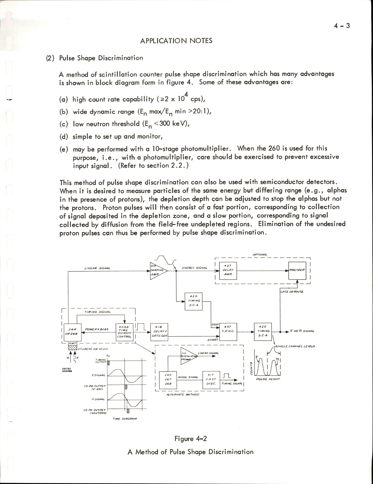
(2)
Pulse
Shape
Discrimination
A
method
of
scintillation
counter
pulse
shape
discrimination
which
has
many
advantages
is
shown
in
block
diagram
form
in
figure
4.
Some
of
these
advantages
are:
4
(a)
high
count
rate
capability
(s2
x
10
cps),
(b)
wide
dynamic
range
ma^v^E^
min
>20:1),
(c)
low
neutron
threshold
(E^^
<300
keV),
(d)
simple
to
set
up
and
monitor,
(e)
may
be
performed
with
a
10-stage
photomultiplier.
When
the
260
is
used
for
this
purpose,
i.e.,
with
a
photomultiplier,
care
should
be
exercised
to
prevent
excessive
input
signal.
(Refer
to
section
2.2.)
This
method
of
pulse
shape
discrimination
can
also
be
used
with
semiconductor
detectors.
When
it
is
desired
to
measure
particles
of
the
same
energy
but
differing
range
(e.g.,
alphas
in
the
presence
of
protons),
the
depletion
depth
can
be
adjusted
to
stop
the
alphas
but
not
the
protons.
Proton
pulses
will
then
consist
of
a
fast
portion,
corresponding
to
collection
of
signal
deposited
in
the
depletion
zone,
and
a
slow
portion,
corresponding
to
signal
collected
by
diffusion
from
the
field-free
undepleted
regions.
Elimination
of
the
undesired
proton
pulses
can
thus
be
performed
by
pulse
shape
discrimination.
£N£l9Cf
SIGNAL
LIN£AR
SIGNAL
VIAPIN
AMP.
AMP.
4
20
TIMING
S.C.A
TIMING
SIGNAL
4
OS
A
TIME
P/CKOPr
CONTROL
26-4
OP
see
POWER*
eiAS
DELAY
4
PM.T.
ST/lBENE
op
NC-^/S
XlHTIUMi
TS/GNAL
ANODC
SIGNAL
PA
ST
DISC.
TIMING
SIGNAL
CO
PO
OUTPUT
(r-
PAY)
ALTERNATE
METNOO
T>
SIGNAL
GATE
OP
ROUTE
4S7
4Z0
T.RH.C.
3.C.A.
OP
"71
SIGNAL
711
PULSE
NEIGNT
CO
PO
OUTPUT
(NCUTPON)
TIME
DIAGRAM
Figure
4-2
A
Method
of
Pulse
Shape
Discrimination
4-
4
APPLICATION
NOTES
(3)
Charged-Particle
Identification
by
Time-of-Flight
The
advent
of
the
260
opens
up
a
new
realm
of
exploration
in
charged-particle
spectroscopy
by
allowing
simultaneous
high-resolution
energy
analysis
and
sub-
nanosecond
time
resolution
measurements
of
charged
particles,
A
block
diagram
of
electronics
needed
to
perform
such
measurements
with
a
pulsed
accelerator
is
shown
in
figure
5.
MODEL
622
PULSED
CHARGE
DETECTOR
ADC
2
ADC
I
50A
260
260
Zo
'
SO
A
Ho
=
50
A
STOP
START
Ho
•
50
A
DELAY
Ho
•
50
A
425
TIME
TO
HEIGHT
CONVERTER
MULTIPARAMETEF
ANALYZER
403A
403A
Figure
4-3
Charged-Particle
Identification
by
Time-of-Flight
4-5
APPLICATION
NOTES
(4)
Beam
Pulse
Time
Pickoff
for
Pulsed
Accelerators
There
are
many
applications
where
timing
experiments
are
performed
with
high-energy
particles.
It
is
sometimes
difficult
to
obtain
a
timing
signal,
indicating
the
time
the
beam
burst
strikes
the
target
(T
=
O),
of
sufficient
accuracy,
and
independent
of
machine
parameters.
A
method
for
obtaining
a
T
=
O
pulse
which
meets
the
criteria
for
accuracy
and
stability,
and
is
also
simple
to
install,
is
shown
in
the
block
diagram
in
figure
6.
The
beam
pulse
pickup
is
an
electrostatic-inductive
pickup
which
is
installed
in
the
beam
tube.
(Further
information
will
be
supplied
upon
request.)
For
this
application,
an
estimate
of
the
required
minimum
beam
pulse
peak
current
(Ip)
may
be
based
upon
V(min),
the
maximum
sensitivity
of
the
260,
which
is
approximately
200pV
into
50
ohms.
Assuming
that
the
pickup
capacitance
(Cp)
is
~5
pF,
we
require,
for
the
minimum
beam
charge
to
provide
the
driving
signal,
Q
(min)
=
C
V
(min)
=
I
A
t
P
P
=
(5
X
10"^^
F)
(2
X
10""^
V)
=
1
X
10"^^
coul.
For
a
pulse
width
of
5
nsec,
this
gives:
I
=Q(raln)
=
2x10"^
A.
p
Z1—
PULSED
BEAM
BEAM
PULSE
PICKUP
SIGNAL
G=)
Zo=
son
A
TARGET
POWER
&
CONTROL
TIMING
SIGNALS
Figure
4-4
Beam
Pulse
Time
Pickoff
System
(T
=
O)
for
Pulsed
Accelerators
5-
1
5.
CIRCUIT
DESCRIPTION
The
circuit
consists
of
a
current
transformer,
two
amplifier
stages,
a
remotely
controlled
tunnel
diode
discriminator,
and
an
emitter
follower
for
a
line
driver
and
buffer.
The
current
pulse
from
a
detector
flows
through
the
transformer
primary,
induces
in
the
sec
ondary
a
corresponding
secondary
current
and
therefore
a
voltage
across
Rj.
Rj
may
take
on
any
value
from
zero
impedance
to
open
circuit,
where
the
input
impedance
will
be
determined
total
ly
by
the
input
impedance
of
Q1
.
Since
Q1
senses
the
voltage
generated
across
the
input
impedance,
the
sensitivity
will
vary
directly
with
Rj.
As
mentioned
at
other
places
in
the
manual,
plug-in
jacks
are
provided
so
that
Ry
may
be
changed.
The
amplifier
must
have
a
negative
input
voltage
at
the
base
of
Ql,
but
since
the
trans
former
primary
has
both
ends
available,
a
signal
of
either
polarity
may
be
processed
by
interchanging
the
role
of
CN-1
and
CN-2.
(Refer
to
section
2.1.)
The
amplifier
consists
of
two
identical
stages,
each
consisting
of
a
fed-back
cascode
driven
by
an
emitter
follower.^
The
first
stage
is
composed
of
Ql,
Q2,
and
Q3,
where
the
degenera
tive
feedback
is
obtained
by
the
10-ohm
emitter
resistor,
R5.
The
bypassing
capacitor,
C4,
serves
to
increase
the
high-frequency
response
without
affecting
the
midfrequency
gain.
The
output
of
the
second
amplifier
stage,
consisting
of
Q5
and
Q6,
feeds
the
tunnel
diode
discriminator,
Dl.
The
bias
current
for
D1
is
derived
from
a
Time
Pickoff
Control
Unit.
The
discriminator
output
pulse
width
may
be
changed,
as
desired,
by
changing
L3,
since
the
pulse
width
is
determined
by
the
L/R
time
constant
composed
of
L3
and
R15.
Plug-in
jacks
are
provided
for
easy
interchange.
Increase
L3
to
obtain
a
wider
pulse.
Q7
is
an
emitter
follower
used
to
drive
the
coaxial
line
and
to
prevent
any
delay-line
reflections
from
retriggering
the
discriminator.
'
C.
W.
Williams
and
J.
H.
Neiler,
IRE
Trans.
Nucl.
Sci.
NS-9
(1962)
p.
1.
6
-
1
6.
MAINTENANCE
INSTRUCTIONS
6.1
Testing
Performance
Many
methods
of
testing
the
unit
may
be
used
for
convenience,
although
only
one
method
will
be
described
here.
The
steps
are
given
for
clarity.
(1)
Connect
the
260
to
the
Time
PIckoff
Control
Unit
as
described
In
sections
3.4
and
3.7.
(2)
Use
a
50-ohm
mercury
switch
delay-line
pulse
generator,
with
the
pulse
width
set
In
the
range
of
2-10
nanoseconds.
Trigger
an
oscilloscope
externally
from
the
pulse
generator
trigger
output.
Attenuate
the
pulser
output
signal
to
obtain
a
negative
5
mV
signal
when
Rj
s
IK
ohms.
(3)
Terminate
CN-2
In
50
ohms.
(4)
Connect
the
pulser
signal
to
CN-1.
(5)
Connect
the
260
output
signal
to
the
Input
of
the
oscilloscope
(terminate
delay
line).
(6)
Turn
on
the
Time
PIckoff
Control
Unit;
there
should
be
an
output
from
the
260
at
this
time.
(7)
Adjust
the
pulser
ourput
to
obtain
an
Input
signal
of
0.3
mV;
the
260
discriminator
should
trigger
on
this
signal
at
a
discriminator
level
setting
above
noise.
(8)
Increase
the
signal
Input
as
desired;
the
threshold
should
cover
a
range
of
15:1
In
signal
amplitude.
6.2
Calibration
Adjustments
The
only
Internal
adjustments
are
Interchange
of
Rj
to
vary
Input
Impedance,
and
Interchange
of
L3
to
vary
output
pulse
width.
6.3
Suggestions
for
Troubleshooting
If
no
output
pulse
Is
obtained,
check
the
cable
connections
between
the
Time
PIckoff
Control
Unit
and
the
Time
PIckoff.
Adjust
the
discriminator
level
control
to
near
zero
and
check
for
output
pulses.
(Discriminator
should
free-run.)
If
the
discriminator
free-
runs,
check
the
Input
connections
for
contact
and
polarity.
If
the
trouble
Is
still
not
located,
perform
a
voltage
check
and
compare
the
results
with
the
values
listed
In
table
3.
Transistor
failures
may
not
be
detected
In
a
voltage
check;
therefore,
transistors
Q1
through
Q6
should
be
tested
separately.
If
the
discriminator
falls
to
free-run,
the
trouble
must
be
discriminator
associated,
so
check
the
voltages
and
compare
them
with
those
In
table
3.
If
the
trouble
Is
still
not
located,
check
the
tunnel
diode,
D1.

6-2
E
-
Emitter
Table
3.
Typical
Voltage
Tests
B
=
Base
ORTEC
260
C
=
Collector
Location
Check
Point
Average
Voltages
P-3
Pin
E
+
11
.9
P-3
Pin
B
-
11.9
B-
bus
-
11.6
B
+
bus
+
11
.5
Q1
E
-
0.7
Q4
E
-
0.88
Q3
B
+
4.7
Q6
B
+
4.9
Q2
E
-
1
.5
Q5
E
-
1.6
Q3
C
+
8.7
Q6
C
+
8.6
Q7
C
-
10.6
Q7
E
+
0.6
Note:
All
voltages
are
read
from
chassis
ground
with
vtvm.
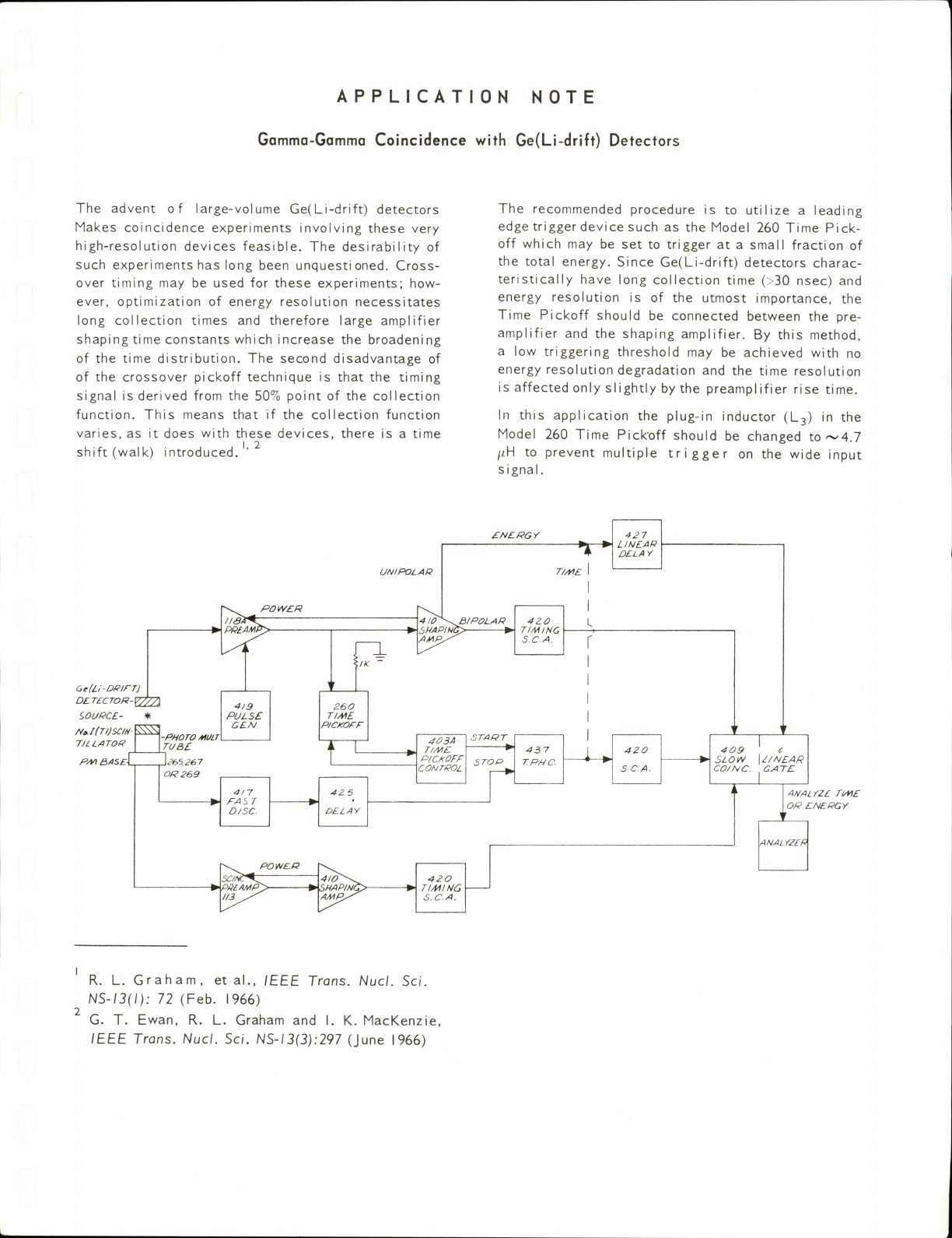
APPLICATION
NOTE
Gamma-Gamma
Coincidence
with
Ge(Li-drift)
Detectors
The
advent
of
large-volume
Ge(Li-drift)
detectors
Makes
coincidence
experiments
involving
these
very
high-resolution
devices
feasible.
The
desirabi
l
ity
of
such
experiments
has
long
been
unquestioned.
Cross
over
timing
may
be
used
for
these
experiments;
how
ever,
optimization
of
energy
resolution
necessitates
long
col
lection
times
and
therefore
large
ampl
ifier
shaping
time
constants
which
increase
the
broadening
of
the
time
distribution.
The
second
disadvantage
of
of
the
crossover
pickoff
technique
is
that
the
timing
signal
is
derived
from
the
50%
point
of
the
col
lection
function.
This
means
that
if
the
collection
function
varies,
as
it
does
with
these
devices,
there
is
a
time
shift
(walk)
introduced.
''^
The
recommended
procedure
is
to
uti
l
ize
a
leading
edge
trigger
device
such
as
the
Model
260
Time
Pick-
off
which
may
be
set
to
trigger
at
a
smal
l
fraction
of
the
total
energy.
Since
Ge(Li-drift)
detectors
charac
teristical
ly
have
long
col
lection
time
(>30
nsec)
and
energy
resolution
is
of
the
utmost
importance,
the
Time
Pickoff
should
be
connected
between
the
pre
ampl
ifier
and
the
shaping
ampl
ifier.
By
this
method,
a
low
triggering
threshold
may
be
achieved
with
no
energy
resolution
degradation
and
the
time
resolution
is
affected
only
slightly
by
the
preampl
ifier
rise
time.
In
this
appl
ication
the
plug-in
inductor
(L3)
in
the
Model
260
Time
Pick'off
should
be
changed
to~4.7
fxH
to
prevent
multiple
trigger
on
the
wide
input
signal.
Ge(Li'DPirT)
DLTCCTOR-YZm
SOURCE-
*
N».l(TI)SaN'^^
rULATOR
P/A
QASE^,
POWER
/IS>
PREAM/
r^r
—
-PHOTO
MULT
TUBE
~\
Ee5.2e7
ENERGY
rZ/HE
427
LINEAR
DELAY
A
POLAR
SHAPihiG:?——►
APR,
420
TIMING
S.CA.
4/9
260
Pulse
T/ME
GEN
P/CKOFF
4/7
PAST
O/SC.
42
6
RELAY
403A
T/ME
P/CNOFF
CONTROL
STOP
437
T.PPC.
4ZO
SC.A.
409
,
^
SLOW
\Z/NEAR
CO/NC.
GATE
r]
A
PfiEAMP
POWER
410
SHAPIM
AMP.
420
TIMING
S.C.A.
NALYZE
T/ME
OR
ENERGY
R.
L.
Graham,
et
al.,
IEEE
Trans.
Nucl.
Sci.
NS-I3(I):
12
(Feb.
1966)
G.
T.
Ewan,
R.
L.
Graham
and
i.
K.
MacKenzie,
IEEE
Trans.
Nucl.
Sci.
NS-I3(3):297
(June
1966)
Table of contents
Other EG&G Measuring Instrument manuals


Popular Measuring Instrument manuals by other brands

Hayward
Hayward TLC SERIES Programming and users manual

MOBILE-ALERTS
MOBILE-ALERTS pro Series quick reference

Bushnell
Bushnell Yardage Pro 20-0750 user guide

JUMO
JUMO flowTRANS MAG S01 operating manual

Symmetricom
Symmetricom TimeAnalyzer 7500 user guide

Kamstrup
Kamstrup MULTICAL 402 Installation and user guide


