EG&G ORTEC 442 Service manual

ORTEC
442
LINEAR
GATE
AND
STRETCHER
REV
442-17
June
28,
1977
On
schematic
442-0101-SI,
change
the
type
designation
of
diode
D7
from
1N3467
to
HPA
1003.
Model
442
Linear
Gate
and
Stretcher
Operating
and
Service
Manual
This
manual
applies
to
instruments
marked
"Rev
16"
on
rear
panel
Printed
in
U.S.A.
2783
(N152QP)
02C
1276

STANDARD
WARRANTY
FOR
ORTEC
INSTRUMENTS
ORTEC
warrants
that
the
items
will
be
delivered
free
from
defects
in
material
or
workmanship.
ORTEC
makes
no
other
warranties,
express
or
implied,
and
specifically
NO
WARRANTY
OF
MERCHANTABILITY
OR
FITNESS
FOR
A
PARTICULAR
PURPOSE.
ORTEC's
exclusive
liability
is
limited
to
repairing
or
replacing
at
ORTEC's
option,
items
found
by
ORTEC
to
be
defective
in
workmanship
or
materials
within
one
year
from
the
date
of
delivery.
ORTEC's
liability
on
any
claim
of
any
kind,
including
negligence,
loss
or
damages
arising
out
of,
connected
with,
or
from
the
performance
or
breach
thereof,
or
from
the
manufacture,
sale,
delivery,
resale,
repair,
or
use
of
any
item
or
services
covered
by
this
agreement
or
purchase
order,
shall
in
no
case
exceed
the
price
allocable
to
the
item
or
service
furnished
or
any
part
thereof
that
gives
rise
to
the
claim.
In
the
event
ORTEC
fails
to
manufacture
or
deliver
items
called
for
in
this
agreement
or
purchase
order,
ORTEC's
exclusive
liability
and
buyer's
exclusive
remedy
shall
be
release
of
the
buyer
from
the
obligation
to
pay
the
purchase
price.
In
no
event
shal
l
ORTEC
be
liable
for
special
or
consequential
damages.
QUALITY
CONTROL
Before
being
approved
for
shipment,
each
ORTEC
instrument
must
pass
a
stringent
set
of
quality
control
tests
designed
to
expose
any
flaws
in
materials
or
workmanship.
Permanent
records
of
these
tests
are
maintained
for
use
in
warranty
repair
and
as
a
source
of
statistical
information
for
design
improvements.
REPAIR
SERVICE
If
it
becomes
necessary
to
return
this
instrument
for
repair,
it
is
essential
that
Customer
Services
be
contacted
in
advance
of
its
return
so
that
a
Return
Authorization
Number
can
be
assigned
to
the
unit.
Also,
ORTEC
must
be
informed,
either
in
writing
or
by
telephone
[(615)
482-4411],
of
the
nature
of
the
fault
of
the
instrument
being
returned
and
of
the
model,
serial,
and
revision
("Rev"
on
rear
panel)
numbers.
Failure
to
do
so
may
cause
unnecessary
delays
in
getting
the
unit
repaired.
The
ORTEC
standard
procedure
requires
that
instruments
returned
for
repair
pass
the
same
quality
control
tests
that
are
used
for
new-production
instruments.
Instruments
that
are
returned
should
be
packed
so
that
they
will
withstand
normal
transit
handling
and
must
be
shipped
PREPAID
via
Air
Parcel
Post
or
United
Parcel
Service
to
the
nearest
ORTEC
repair
center.
The
address
label
and
the
package
should
include
the
Return
Authorization
Number
assigned.
Instruments
being
returned
that
are
damaged
in
transit
due
to
inadequate
packing
will
be
repaired
at
the
sender's
expense,
and
it
will
be
the
sender's
responsibility
to
make
claim
with
the
shipper.
Instruments
not
in
warranty
will
be
repaired
at
the
standard
charge
unless
they
have
been
grossly
misused
or
mishandled,
in
which
case
the
user
will
be
notified
prior
to
the
repair
being
done.
A
quotation
will
be
sent
with
the
notification.
DAMAGE
IN
TRANSIT
Shipments
should
be
examined
immediately
upon
receipt
for
evidence
of
external
or
concealed
damage.
The
carrier
making
delivery
should
be
notified
immediately
of
any
such
damage,
since
the
carrier
is
normally
liable
for
damage
in
shipment.
Packing
materials,
waybills,
and
other
such
documentation
should
be
preserved
in
order
to
establish
claims.
After
such
notification
to
the
carrier,
please
notify
ORTEC
of
the
circumstances
so
that
assistance
can
be
provided
in
making
damage
claims
and
in
providing
reolacement
equipment
if
necessary.

Ill
CONTENTS
Page
WARRANTY
ii
PHOTOGRAPHS
iv
1.
DESCRIPTION
1
2.
SPECIFICATIONS
1
3.
INSTALLATION
2
3.1.
Connection
to
Power
3.2.
Linear
Input
Connection
3.3.
Linear
Output
Connections
3.4.
Gate
Input
3.5.
Connection
for
Busy
Output
2
3
3
3
3
4.
OPERATION
4.1.
Selection
of
Input
Circuit
4.2.
Discriminator
Level
Adjustment
4.3.
Output
Delay
Adjustment
4.4.
Output
Width
Adjustment
4.5.
Output
DC
Adjustment
4.6.
Gated
Operation
4.7.
Overall
Logic
4
4
4
4
4
4
4
5.
CIRCUIT
DESCRIPTION
5
5.1.
DC
Restorer
5.2.
Buffer
Amplifier
5.3.
Input
Gate
5.4.
Busy
Output
5.5.
Discriminator
5
6
6
6
7
5.6.
Stretch
Amplifier
5.7.
Output
Pulse
Delay
Control
5.8.
Output
Pulse
Width
Control
5.9.
Output
Gate
5.10.
Output
Driver
Amplifier
6.
MAINTENANCE
6.1.
Testing
Performance
of
Pulse
Stretcher
6.2.
Calibration
Procedures
6.3.
Suggestions
for
Troubleshooting
6.4.
Tabulated
Test
Point
Voltages
on
Etched
Board
8
9
9
SCHEMATIC
442-0101-S1
ILLUSTRATIONS
Fig.
5.1.
Block
Diagram
of
Model
442
Linear
Gate
and
Stretcher
Fig.
5.2.
Typical
Timing
Diagram
of
442
in
Normal
Condition
Fig.
5.3.
Typical
Timing
Diagram
of
Model
442
Showing
Effect
of
Eliminating
Pulse
Pileup
5
6
6

LINEAR.
GATE
STRETCHER
COUPLE.
'
LEVEL
M
OUTPUT
—r
LY
.
WIDTH
,
m
SEI?.
ii
93
0
y
OUTPUT
BUr,Y
OUTPUT
COINC.
I
ANTI
COINC

ORTEC
442
LINEAR
GATE
AND
STRETCHER
1.
DESCRIPTION
The
ORTEC
442
Linear
Gate
and
Stretcher
is
designed
to
increase
the
duration
of
short
input
pulses
by
stretching
their
peak
ampl
itudes
for
a
required
minimum
pulse
width.
This
effectively
reduces
the
bandwidth
requirements
of
analog-to-digital
converters
in
multichannel
pulse
height
analyzers
and
improves
the
resulting
l
inearity.
The
linear
gate
included
in
the
442
permits
selective
control
of
the
acceptance
of
input
pulses,
and
is
also
used
to
prevent
positive-on-positive
pulse
pileup.
The
442
accepts
l
inear
signals,
during
its
permissive
gating
periods,
from
any
l
inear
source
and
reshapes
the
input
signal
as
required
to
provide
a
suitable
waveform
into
a
circuit
that
measures
the
peak
amplitude.
Any
reshaping
of
the
input
pulse
must
retain
the
l
inear
parameter
of
the
input
signal,
which
is
its
relative
peak
ampl
itude.
The
pulse
width
of
the
input
is
unimportant
except
from
the
practical
viewpoint
of
having
the
peak
amplitude
exist
long
enough
to
permit
accurate
response
and
measurement.
The
input
gate
can
be
controlled
from
an
external
source,
and
operated
in
either
a
coincidence
or
an
anticoincidence
mode.
The
Gate
Period
generator
wi
l l
be
triggered
on
the
leading
edge
of
a
gate
input
pulse
and
continue
for
the
effective
period
set
by
the
front
panel
adjustment.
The
Gate
Period
must
overlap
the
linear
input
pulse
peak
for
coinci
dence
mode
operation
or
must
overlap
the
discriminator
response
for
anticoincidence
mode,
A
l
inear
input
pulse
must
exceed
the
adjusted
discriminator
level
to
initiate
a
response
in
the
442.
When
the
discrimina
tor
fires,
it
initiates
the
stretch
action
unless
the
gate
control
is
in
the
external
coincidence
mode
and
a
gate
pulse
IS
not
present.
The
input
gate
remains
open
only
until
the
peak
of
the
l
inear
pulse
has
been
detected,
and
then
is
again closed
to
prevent
pileup.
An
output
pulse
wi
ll
be
generated
if
a
peak
is
detected,
and
wil
l
occur
at
an
adjusted
delay
following
the
input
peak
for
an
adjusted
width.
Both
the
delay
and
width
adjustments
are
front
panel
controls
on
the
442.
The
input
gate
cannot
be
opened
again
until
the
output
pulse
has
been
completed
and
the
l
inear
input
pulse
has
permitted
the
discriminator
to
reset.
This
internal
logic
prevents
pulse
pi
leup
and
false
ampl
itude
outputs
for
the
system.
Short-duration
linear
pulses
are
associated
normally
with
biased
ampl
ifiers.
The
442
can
be
used
in
this,
or
any
other,
system
to
assure
an
adequate
duration
of
the
peak
amplitude
where
a
pulse
width
might
be
too
short
or
where
the
width
variations
would
otherwise
produce
a
nonlinear
response
or
measurement.
It
may
be
used
at
any
point
in
the
l
inear
system
after
a
basic
linear
ampl
ifier,
and
its
gating
function
permits
logical
placement
directly
after
the
linear
amplifier.
For
best
system
performance
tne
442
should
precede
the
biased
amplifier.
2.
SPECIFICATIONS
PERFORMANCE
LINEAR
INPUT
AMPLITUDE
+0
1
to
+10
V,
l
inear
range;
±12
V
maximum.
LINEAR
INPUT
RISE
TIME
100
nsec
to
10
/tisec.
LINEAR
OUTPUT
WIDTH
0.5
to
5/usec.
LINEAR
OUTPUT
DELAY
0.3
to
3
/ttsec
after
input
pulse
peak.
GAIN
Unity
(
nominal).
INTEGRAL
NONLINEARITY
<0.1%
for
pulse
rise
time
>100
nsec
and
pulse
width
>400
nsec.
TEMPERATURE
INSTABILITY
Gain
shift
<0.01%/°C,
0
to
50'C.
COUNTING
RATE
dc-couplea
throughout
when
DC
Couple
input
is
selected.
The
centroid
of
a
pulser
spectrum
at
85%
of
full
scale
wi
ll
shift
<0.1%
when
modulated
by
5
x
10"
counts/sec
of
random
signals
from
'^''Cs
source-detector
combination
\/vith
photopeak
at
70%
of
full
scale
(DC
Couple
mode
and
amplifier
shaping
time
T
=
1
/isec).
When
dc
restorer
modes
are
used,
count
rate
is
dependent
on
shaping
ampl
ifier
time
constants
and
pulse
undershoot.
CONTROLS
The
fol
lowing
controls
are
on
the
front
panel
:
DC
COUPLE
3-position
sl
ide
switch,
selects
input
circuit
desired:
BLR
High,
BLR
Low,
or
DC
Couple.
DISC
LEVEL
Screwdriver
potentiometer;
adjusts
sen
sitivity
level
for
input
discriminator;
range
+0.1
to
+1
V;

discriminator
remains
triggered
while
input
level
exceeds
adjusted
sensitivity.
OUTPUT
DELAY
Screwdriver
potentiometer:
adjusts
delay
period
from
input
pulse
peak
to
start
of
output
pulse;
range
0.3
to
3
fisec.
OUTPUT
WIDTH
Screwdriver
potentiometer,
adjusts
width
of
the
output
pulse;
range
0.5
to
5
iisec.
NORMAL/GATED
Sl
ide
switch
selects
exclusion
(Normal)
or
inclusion
(Gated)
of
external
gating
function.
GATE
PERIOD
Screwdriver
potentiometer,
adjusts
dura
tion
of
gating
control
from
leading
edge
of
Gate
Input
pulse;
range
0.5
to
5
^isec;
includes
test
point
for
monitor
ing
adjusted
gate
period.
OUTPUT
DC
ADJ
Screwdriver
potentiometer,
permits
adjustment
of
output
dc
level
between
±1.5
V.
The
fol
lowing
control
is
on
the
rear
panel
:
COINC/ANTICOINC
Sl
ide
switch
selects
effective
mode
for
Gate
Input
function.
INPUTS
LINEAR
INPUT
Type
BNC
connector,
front
panel.
Polarity
Positive
unipolar,
or
bipolar
with
positive
portion
leading.
Amplitude
-t-0.1
to
-HO
V;
±12
V
maximum.
Rise
Time
1
GO
nsec
to
10
jusec.
Impedance
~1000J2.
GATE
INPUT
Type
BNC
connector,
front
panel,
for
optiortal
external
control
for
switch-selectable
coincidence
or
anticoincidence
mode
triggering.
Standard
NIM
slow
logic
pulse,
triggers
selected
gate
function
at
+3
V
(100
nsec
minimum
width),
protected
to
±25
V.
OUTPUTS
OUTPUT
Front
panel
type
BNC
connector;
furnishes
linear
positive
output
pulses
through
Zq
<
1J2;
includes
test
point.
Polarity
Positive.
Amplitude
+0.1
to
+10
V,
equal
to
peak
of
the
accepted
linear
input
pulse.
Delay
Adjust
by
front
panel
control;
range
0.3
to
3
nsec
after
input
pulse
peak.
Rise
Time
300
nsec.
Width
Adjusted
by
front
panel
control;
range
0.5
to
5
/isec.
Impedance
<1
fZ
on
front
panel
.
Nonlinearity
<0.1%
with
pulse
amplitude
droop
<0.5
mV/
jjsec.
Baseline
Adjust
±1.5
V.
93J2
OUTPUT
Rear
panel
type
BNC
connector
furnishes
the
l
inear
positive
output
pulses
through
Zg
=
93T2.
BUSY
OUTPUT
Rear
panel
type
BNC
connector
furnishes
+5
V
nominal
through
Zg
<
lOJiZ
through
al
l
periods
when
input
pulses
cannot
be
accepted;
may
be
used
to
control
external
equipment
or
for
monitoring
internal
ly
created
dead
time.
Busy
+5
V
nominal
when
l
inear
pulse
cannot
be
accepted.
Not
Busy
0
V
nominal
when
l
inear
pulse
can
be
accepted.
ELECTRICAL
AND
MECHANICAL
POWER
REQUIREMENTS
+24
V,
69
mA;
+12
V,
75
mA;
-24
V,
76
mA;
-12
V,
14
mA.
WEIGHT
(Shipping)
4
lb
(1
.9
kg).
WEIGHT
(Net)
2
lb
(0.9
kg).
DIMENSIONS
NIM-standard
single-width
module
(1.35
by
8.714
in.)
per
TID-20893
(Rev.).
3.
INSTALLATION
The
442
contains
no
internal
power
supply
but
is
designed
for
instal
lation
in
a
standard
Bin
and
Power
Supply,
such
as
one
of
the
ORTEC
401/402
Series,
which
is
intended
for
rack
mounting.
Therefore
if
vacuum
tube
equipment
is
operated
in
the
same
rack,
there
must
be
adequate
cooling
air
circulating
to
prevent
any
localized
heating
of
the
442
transistorized
circuits.
The
temperature
of
equipment
mounted
in
racks
can
easily
exceed
the
recommended
maximum
unless
precautions
are
observed.
The
ORTEC
442
should
not
be
subjected
to
temperatures
in
excess
of
120°F(50°)
.
3.1.
CONNECTION
TO
POWER
Always
turn
off
power
for
the
Bin
and
Power
Supply
before
inserting
or
removing
any
modules.
The
ORTEC
400
Series
of
modular
instruments
are
designed
so
that
it
is
not
possible
to
overload
the
Power
Supply
with
a
ful
l
complement
of
modules
in
the
Bin.
Since,
however,
this
may
not
be
true
when
the
Bin
contains
modules
other
than
those
of
ORTEC
design,
check
the
Power
Supply
for
any
overload
conditions
by
testing
the
dc
power
levels
after
al
l
modules
are
inserted.

The
ORTEC
442
may
be
operated
outside
the
401/402
Bin
and
Power
Supply,
using
a
power
extension
cable.
Be
sure
that
the
cable
used
accounts
properly
for
the
grounding
circuits
recomrrtended
in
AEC
standards
of
TID-20893
(Rev.).
Both
clean
and
dirty
ground
connections
are
included
to
ensure
proper
reference
voltage
feedback
into
the
Power
Supply
and
must
be
preserved
by
the
remote
cable.
Be
careful
to
avoid
ground
loops
when
the
module
is
operated
outside
the
Bin.
3.2
LINEAR
INPUT
CONNECTION
Linear
input
pulses
can
be
furnished
from
any
ORTEC
linear
module
of
the
400
Series.
These
include
amplifiers,
delay
circuits,
biased
amplifiers,
gates,
and
other
pulse-
handling
equipment.
It
is
recommended
that
the
442
be
used
ahead
of
the
biased
amplifier
when
both
modules
are
used
in
a
system.
The
effective
input
range
will
be
from
the
adjusted
discriminator
level
(-tO.1
to
1
V)
up
through-i-lO
V.
When
the
linear
input
signals
are
furnished
through
a
cable
more
than
4
ft
long
(approximately),
the
input
should
be
terminated
with
the
characteristic
impedance
of
the
cable.
This
can
usually
be
avoided
by
the
use
of
shorter
cable
lengths.
3.3.
LINEAR
OUTPUT
CONNECTIONS
The
shaped
linear
output
pulses
can
be
furnished
into
any
other
ORTEC
Series
400
linear
module
or
directly
into
the
ADC
input
of
a
multichannel
analyzer.
It
is
important
to
preserve
the
pulse
shape
and
linear
ampl
itude
relationship
of
the
output,
as
it
appears
when
accepted
into
subsequent
instrument
modules.
Either
of
two
standard
output
imped
ances
may
be
selected
according
to
the
type
and
length
of
interconnecting
cable
and
the
input
impedance
of
the
instru
ment
to
which
it
is
connected.
The
output
is
available
through
a
front
panel
connector,
with
an
output
imped
ance
of
less
than
112,
or
through
a
rear
panel
connector,
with
Zo
=
9312.
For
most
appl
ications
the
112
front
panel
output
connector
can
be
used,
with
a
short
cable
length,
to
transfer
the
output
signal
into
the
(normally)
high
input
impedance
of
the
next
module.
When
the
output
signals
must
be
furnished
through
cable
lengths
greater
than
approximately
4
ft,
proper
resistive
termination
of
the
cable
is
required
in
order
to
preserve
the
linear
output
pulses
and
prevent
oscillations.
Either
of
two
convenient
methods
can
be
selected
for
the
442
outputs,
when
termination
is
required.
One
method
is
a
series
type
termination,
using
the
rear
panel
9312
Output
connector
and
an
appropriate
length
of
9312
coaxial
cable
to
transfer
the
signal
into
the
next
module
or
instrument.
The
input
impedance
of
the
next
equipment
wil
l
probably
be
of
the
order
of
100012
or
more.
The
total
amplitude
of
each
output
pulse
will
be
divided
between
the
9312
output
impedance
of
the
442
and
the
input
impedance
of
the
next
module;
so
a
high
input
impedance
is
desirable
when
this
series-termination
method
is
used.
An
alternate
method
depends
upon
shunt
termination
at
the
remote
end
of
the
cable.
For
this,
use
the
front
panel
112
Output
connector
and
whatever
type
of
coaxial
cable
is
desired.
Then
use
a
BNC
tee
at
the
input
to
the
next
module
to
accept
both
the
cable
and
a
BNC
Terminator,
selected
to
match
the
charac
teristic
impedance
of
the
cable
when
connected
in
parallel
with
the
instrument's
input
impedance.
For
convenience,
ORTEC
stocks
a
limited
quantity
of
BNC
tee
connectors,
and
both
50
and
10012
BNC
Terminators.
3.4.
GATE
INPUT
When
Gate
Input
signals
are
required,
they
will
be
furnished
through
the
BNC
connector
on
the
front
panel
of
the
442.
The
function
of
an
input
pulse
will
be
to
trigger
the
442
Linear
Input
gate
for
an
adjusted
Gate
Period.
The
function
must
be
selected
as
either
Coinc
or
Anticoinc
by
a
rear
panel
slide
switch.
Gate
Input
pulses
are
effective
when
they
rise
through
-)-3
V
for
a
period
of
at
least
100
nsec.
A
standard
NIM
Slow
Logic
positive
pulse
source
may
be
used.
The
Gate
Input
circuit
is
protected
to
±25
V;
so
a
wide
variety
of
alternate
sources
can
also
be
used
to
initiate
this
control.
When
operating
in
the
Coinc
mode,
the
Gate
Period
must
be
triggered
before
the
peak
of
the
linear
input
pulse
and
must
be
continued
until
after
the
peak.
When
operating
in
the
Anticoinc
mode,
the
Gate
Period
must
be
triggered
prior
to
a
discriminator
response
to
the
linear
input
and
must
be
continued
until
the
discriminator
has
been
reset.
No
Gate
Input
is
required
if
the
front
panel
Normal/Gated
switch
is
set
at
Normal.
Likewise,
if
the
front
panel
switch
is
set
at
Gated
and
the
rear
panel
mode
selector
is
set
at
Anticoinc,
a
Gate
Input
pulse
is
not
required
except
when
a
linear
input
signal
is
to
be
rejected.
Whan
these
switches
are
set
for
Gated
and
Coinc,
respectively,
a
linear
input
pulse
will
be
accepted
only
if
it
is
accompanied
by
a
time
coincident
Gate
Input
pulse.
3.5.
CONNECTION
FOR
BUSY
OUTPUT
The
duration
of
each
Busy
Output
signal
is
from
the
time
that
an
input
pulse
peak
is
detected
unti
l
the
resulting
output
pulse
has
been
furnished
and
the
input
discriminator
has
been
reset.
This
identifies
each
period
during
which
a
new
input
pulse
cannot
be
accepted
in
the
442.
This
output
can
be
integrated
externally
to
indicate
the
average
dead
time.

4.
OPERATION
4.1.
SELECTION
OF
INPUT
CIRCUIT
Any
of
three
oircuit
connections
can
be
selected
with
the
sl
ide
switch
at
the
top
of
the
front
panel
:
DC
Couple,
BLR
(Base
Line
Restorer)
Low,
or
BLR
High,
The
proper
selection
wi
l l
depend
on
the
type
of
output
circuit
In
the
module
from
which
the
l
inear
input
pulses
are
furnished
to
the
442
and
on
the
relative
counting
rate.
The
DC
Couple
switch
position
provides
an
optimum
signal
transfer
circuit
with
lOOOO
Input
impedance
If
the
pulses
are
furnished
from
an
ampl
ifier
with
a
dc-coupled
output
and
a
properly
adjusted
zero
basel
ine.
If
the
source
does
not
include
baseline
restoration,
use
a
capacitive
coupling
into
the
442
and
select
either
Low
or
High
BLR
In
the
442.
For
an
ac-coupled
signal
input,
select
one
of
the
dc-restorer
Input
circuits
In
the
442.
There
Is
no
precise
dividing
l
ine,
because
of
the
various
shaping
time
constants
which
may
be
affecting
the
pulse
shape
furnished
to
the
442.
For
1-^tsec
pulses
the
division
Is
approximately
15,000
counts/sec.
If
bipolar
pulses
are
applied
to
the
input
the
DC-Couple
or
BLR
Low
configurations
must
be
selected.
The
most
practical
method
of
selecting
between
High
and
Low
is
observation
of
the
Output,
using
the
circuit
that
provides
the
better
results.
4.2.
DISCRIMINATOR
LEVEL
ADJUSTMENT
The
Disc
Level
adjustment
is
for
the
purpose
of
preventing
response
to
all
noise
pulses.
Therefore,
it
should
be
adjusted
high
enough
in
its-i-O.I-to
TV
range
to
ensure
discrimination
against
the
maximum
noise
amplitude
that
may
exist
at
the
input
to
the
442
In
the
system.
Since
the
logic
in
the
442
prevents
response
to
a
new
input
pulse
unti
l
the
Disc
Level
has
been
reset
but
permits
acceptance
at
that
time
unless
an
output
pulse
has
not
been
completed,
too
high
a
setting
of
the
Disc
Level
can
permit
a
small
amount
of
pileup
to
occur
If
the
input
pulse
has
a
very
long
time
constant
decay.
Although
this
Interference
Is
possible.
It
Is
unl
ikely
In
most
applications.
Sti
l l
,
an
un
necessari
ly
high
adjustment
is
not
recommended.
4.3.
OUTPUT
DELAY
ADJUSTMENT
The
adjustment
of
the
Output
Delay
permits
a
control
for
normal
izing
timing
in
the
system
in
which
the
442
Is
Included.
The
delay
period
is
measured
from
the
time
that
the
internal
stretch
amplifier
senses
a
peak
ampl
itude
in
the
accepted
linear
input
pulse
and
is
adjustable
through
the
range
of
0.3
to
3
^tsec.
At
the
end
of
the
delay
period
the
output
gate
Is
opened
and
an
output
pulse
is
furnished
to
the
next
Instrument
In
the
system.
4.4.
OUTPUT
WIDTH
ADJUSTMENT
The
purpose
of
this
stretch
circuit
is
to
provide
an
output
pulse
with
a
fixed
and
known
width.
The
range
of
the
control
is
0.5
to
5
usec,
and
its
proper
setting
wil
l
be
determined
by
the
Input
requirements
of
subsequent
Instruments
In
the
system.
Each
output
pulse
wil
l
have
the
adjusted
width,
regardless
of
the
wldth(s)
of
l
inear
pulses
furnished
to
the
442
input.
4.5.
OUTPUT
DC
ADJUSTMENT
In
normal
usage
the
quiescent
level
for
the
output,
through
both
the
front
and
rear
panel
connectors,
should
be
at
ground
potential
.
Use
the
test
point
for
the
front
panel
Output,
and
adjust
the
screwdriver
control
as
necessary
to
set
the
level
at
ground
potential
when
there
are
no
output
signals.
When
the
DC
Input
is
used
on
some
analyzers
it
is
necessary
that
the
signal
source
have
a
quiescent
dc
level
other
than
zero;
when
the
442
is
used
In
such
applications
adjust
the
output
dc
level
as
required.
4.6.
GATED
OPERATION
No
Gate
Input
pulse
is
required
if
the
front
panel
slide
switch
is
set
at
Normal
.
Likewise,
if
the
slide
switch
Is
set
at
Gated
and
the
mode
selector
on
the
rear
panel
is
set
for
Antlcolnc,
linear
input
pulses
will
be
accepted
when
there
is
no
signal
through
the
Gate
Input
connector.
Whenever
a
signal
is
furnished
through
the
Gate
Input
with
gated
Antlcolnc
effective,
al
l l
inear
Input
signals
are
inhibited
throughout
the
Gate
Period.
To
be
effective,
the
Gate
Period
must
be
adjusted
to
overlap
the
period
of
dis
criminator
response
to
any
pulse
that
Is
to
be
Inhibited
by
the
Anticoinc
signal;
if
the
l
inear
input
triggers
the
discriminator
before
the
Gate
Input
or
if
the
Gate
Period
terminates
prior
to
discriminator
recovery,
there
wi
ll
be
an
output,
but
the
ampl
itude
wil
l
not
usual
ly
duplicate
a
peak
Input
ampl
itude.
When
the
442
is
set
for
gated
coincidence
operation,
a
l
inear
Input
signal
is
accepted
for
stretching
If
and
only
If
there
Is
a
time-coincident
Gate
Input.
The
Gate
Input
signal
must
occur
before
the
peak
amplitude
of
the
l
inear
input
pulse,
and
the
Gate
Period
must
be
long
enough
to
continue
the
control
beyond
the
internal
detection
of
the
peak
ampl
itude.
Refer
to
Section
6.2
for
l
inear
gate
pedestal
adjustment
procedures.
4.7.
OVERALL
LOGIC
When
an
Input
pulse
arrives
at
the
Linear
Input,
It
Is
appl
ied
directly
to
the
discriminator.
As
Its
ampl
itude
rises
through

the
discriminator
threshold,
the
discriminator
may
be
fired
or
it
may
sti
l l
be
set
because
of
not
having
recovered
from
a
previous
input
pulse.
The
linear
input
pulse
will
not
be
accepted
unless
the
discriminator
has
recovered
prior
to
the
new
pulse;
it
wi
ll
also
be
rejected
if
(1)
an
out
put
pulse
has
not
been
completed
for
a
previously
accepted
input;
(2)
the
operating
mode
is
gated
coinci
dence
and
no
Gate
Input
has
been
furnished;
or
(3)
the
operating
mode
is
gated
anticoincidence,
a
Gate
Input
signal
has
been
furnished,
and
the
Gate
Period
is
in
effect.
When
the
discriminator
recovers,
it
will
permit
the
input
to
be
gated
on
unless
(1)
the
output
pulse
has
not
been
completed
or
(2)
external
Gate
Input
logic
has
closed
the
l
inear
input
circuit.
When
the
output
pulse
has
been
completed,
the
l
inear
input
is
permissive
unless
(1)
the
discriminator
is
not
reset
or
(2)
external
Gate
Input
logic
has
closed
the
l
inear
input
circuit.
When
the
discriminator
is
triggered
prior
to
a
Coincidence
Gate
Input
but
the
l
inear
input
is
otherwise
permissive,
the
l
inear
input
signal
is
not
appl
ied
to
the
stretch
circuit
until
the
Gate
Input
signal
is
furnished.
Under
these
con
ditions,
the
l
inear
input
signal
is
applied
to
the
stretch
circuit
at
the
Gate
Input
time;
an
output
signal
will
result,
which
has
an
ampl
itude
equal
to
(1)
the
peak
input
ampl
itude
or
(2)
the
input
ampl
itude
at
the
end
of
the
adjusted
Gate
Period
(whichever
occurs
first).
Thus,
it
is
important
that
the
gate
be
triggered
during
the
rise
time
of
the
l
inear
input
pulse
and
that
it
remain
effective
until
after
the
peak
ampl
itude
has
been
sensed.
5.
CIRCUIT
DESCRIPTION
This
section
provides
a
brief
description
of
the
basic
functions
of
the
442
and
the
circuit
diagram.
Reference
is
frequently
made
to
Fig.
5.1
and
to
schematic
442-0101-SI
(at
the
back
of
the
manual).
5.1.
DC
RESTORER
The
input
section
of
the
442
is
a
dc
restorer
that
can
be
by-passed
by
selecting
DC-Couple
with
switch
SI.
If
dc
BIK
LOW
restoration
is
desired,
restoration
can
be
selected
for
either
a
low
or
high
count
rate
by
SI.
The
low
restoration
rate
is
approximately
5
mV//isec,
and
the
high
rate
is
approxi
mately
150
mV/^isec.
The
restoration
currents
for
the
low
and
high
modes
are
approximately
100
ijlA
and
3
mA
respectively.
The
restoration
rate
can
be
readi
ly
changed
by
changing
the
vaiue
of
C1.
The
restoration
circuit
is
composed
of
Q1,Q2,
Q58,
and
Q59.
OUTPUT
oil!
UIGH
STRETCH
AMP
RESTORER
COUPLE
ADJUST
BUFFER
ANTi-CQiNC
CONTROL
PULSE
DELAY
AOi.
PULSE
WIDTH
AOI.
LOGIC
.
R
94
Fig.
5.1.
Block
Diagram
of
Model
442
Linear
Gate
and
Stretcher.

5.2.
BUFFER
AMPLIFIER
The
restoration
circuit
is
followed
by
a
noninverting
buffer
ampl
ifier
(Q3-Q6)
with
a
gain
of
approximately
1.
T
h
e
g
a
i
n
of
this
stage
is
given
by
the
r
a
t
i
o
o
f
(RIO
+
R117)/R1Q.
The
442
is
dc-coupled
from
this
stage
to
the
output:
so
an
adjustment
is
provided
in
each
stage
to
adjust
its
dc
level
to
zero.
Potentiometer
R7
should
be
adjusted
so
that
the
output
dc
level
of
the
buffer
ampl
ifier
(TP1)
is
zero
volts.
The
buffer
amplifier
drives
the
input
gate
and
the
discriminator.
5.3.
INPUT
GATE
Transistor
Q7
is
a
shunt-type
Input
Gate.
When
the
front
panel
Mode
switch
is
set
at
Normal,
Q7
remains
off
until
the
peak
of
the
input
pulse
has
been
sensed;
at
the
peak
detection,
Q7
saturates
and
clamps
the
gate
of
Q8
to
ground.
No
further
input
conditions
wil
l
affect
the
input
circuit
until
the
Q7-Q8
condition
has
been
restored,
and
this
prevents
positive-on-positive
pulse
pileup.
The
Q7-Q8
condition
will
be
reset
only
after
the
input
signal
fal
ls
below
the
discriminator
level
and
the
442
Output
pulse
has
been
completed.
The
normal
timing
relations
in
the
442
are
shown
in
Fig.
5.2,
with
the
Busy
Output
time
extending
from
the
input
peak
to
the
decay
of
the
Linear
Output
pulse,
and
the
input
gate
is
automatically
inhibited
through
this
Busy
interval
.
Figure
5.3
shows
pileup
rejection
of
a
second
input
pulse
because
the
second
pulse
prevents
reset
of
the
discriminator
in
the
442
until
a
time
after
the
Linear
Output
has
been
completed,
and
the
Busy
interval
is
extended
until
the
discriminator
has
been
reset.
The
internal
gating
control
is
independent
of
the
coincidence
or
anticoincidence
logic
that
may
also
be
appl
ied
from
an
external
source.
Input
Linear
Pulse
Disc.
Output
Delay
Pulse
Width
Pulse
Input
Gate
|normj
Q7
Busy
Output
Stretch
Amp.
Output
442
Linear
Output
Fig.
5.2.
Typical
Timing
Diagram
of
442
in
Normal
Condition.
OiSG.
Lenil
Input
Linear
Pulses
Disc.
Out
Delay
Pulse
Width
Pulse
Input
Gate
|norm|
Q7
Busy
Output
Stretch
Amp.
Output
442
Linear
Output
Fig.
5.3.
Typical
Timing
Diagram
of
Model
442
Showing
Effect
of
Eliminating
Pulse
Pileup.
When
the
Normal/Gated
switch
is
in
the
Gated
position
and
the
Coinc-Anticoinc
switch
is
in
the
Coinc
position,
Q7
will
normal
ly
be
turned
on
and
saturated,
clamping
the
gate
of
Q8
to
ground.
In
order
to
open
the
gate
by
turning
off
Q7,
a
logic
pulse
must
be
appl
ied
to
the
Gate
Input
BNC.
This
pulse
is
reshaped
to
a
desired
Gate
Period
by
IC5,
Q56,
and
Q57
and
appl
ied
to
the
input
gate
drive
circuitry
(Q41-Q43)
to
open
the
gate
(Q7)
for
the
time
of
the
gate
period.
The
gate
period
must
overlap
the
peak
of
the
linear
pulse
in
order
for
the
442
to
function
properly.
If
the
Anticoinc
position
is
selected,
Q7
wi
l l
act
in
an
inverse
manner
to
its
operation
in
the
Coinc
mode;
Q7
will
normally
be
off
(gate
open)
except
during
the
gate
period,
at
which
time
it
will
be
saturated
(gate
closed).
In
order
for
the
442
to
operate
properly
in
the
Anticoinc
mode,
the
Gate
Period
pulse
must
totally
overlap
the
time
that
the
l
inear
input
is
above
the
discrimination
level
for
the
pulse
to
be
blocked.
The
range
of
the
Gate
Period
circuit
can
be
changed
by
changing
the
value
of
C45.
5.4.
BUSY
OUTPUT
The
Busy
Output
is
a
measure
of
the
internal
ly
created
dead
time
of
the
442.
This
signal
begins
at
the
peak
of
the
linear
pulse
and
ends
at
the
completion
of
the
442
output
pulse
if
the
input
is
below
the
discriminator
level
.
Refer
to
timing
diagrams
in
Figs.
5.2
and
5.3.

5.5.
DISCRIMINATOR
The
discriminator
permits
the
442
to
reject
all
input
pulses
that
fall
below
the
discriminator
level
selected,
i
.e.,
noise
pulses.
The
discriminator
level
can
be
varied
from
0.1
V
to
1
V
by
a
front
panel
potentiometer,
R75.
If
the
discrimina
tor
level
is
exceeded
by
an
input
pulse
and
the
proper
gating
pulses
are
appl
ied
when
operating
in
the
gated
mode,
a
signal
is
sent
to
the
stretch
ampl
ifier,
switching
the
current
in
Q23
and
Q24
and
causing
the
input
pulse
to
be
stretched.
5.6.
STRETCH
AMPLIFIER
The
stretch
amplifier
is
a
noninverting
amplifier
composed
of
transistors
Q8-Q25.
Q24
is
normal
ly
conducting,
causing
current
to
flow
in
D5
and
keeping
the
ampl
ifier
loop
closed.
When
the
input
pulse
exceeds
the
discriminator
level,
the
current
in
Q24
is
switched
to
Q23.
The
stretch
capacitor,
C17,
is
charged
through
D5
to
the
peak
voltage
of
the
input
pulse.
After
the
peak
voltage
occurs,
D5
is
back-biased
and
the
peak
voltage
is
stored
on
C17
until
Q24
is
switched
on
again
at
the
end
of
the
output
pulse.
A
high-input-impedance
noninverting
amplifier,
Q13-Q18,
acts
as
a
buffer
and
driver
for
the
voltage
on
capacitor
C17.
This
ampl
ifier
is
included
inside
the
stretch
amplifier
loop
to
provide
better
l
inearity
and
stability.
Q20-Q22
monitors
the
voltage
across
D5
and
produces
a
peak
detect
signal
when
D5
transitions
to
the
back-biased
condition.
The
peak
detect
pulse
is
routed
to
the
control
logic
to
initiate
the
delay
and
output
width
signals.
Potentiometer
R18
is
provided
to
adjust
the
voltage
at
TP2
to
zero
volts
when
the
input
voltage
to
Q8
is
zero.
5.7.
OUTPUT
PULSE
DELAY
CONTROL
The
delay
circuit
consists
of
Q48, Q49,
and
two
gates
in
ICS.
The
leading
edge
of
the
peak
detect
signal
initiates
the
delay
circuit,
causing
it
to
produce
a
pulse
of
width
determined
by
the
setting
of
R94.
The
width
of
the
delay
pulse
can
be
varied
from
300
nsec
to
3
fjsec
by
varying
the
setting
of
R94.
The
delay
range
can
be
increased
by
increasing
the
value
of
C32.
5.8.
OUTPUT
PULSE
WIDTH
CONTROL
The
delay
pulse
is
routed
to
the
output
pulse
width
control
circuit
(Q46,
Q47,
and
two
gates
in
IC4).
The
trailing
edge
of
the
delay
pulse
energizes
the
width
circuit,
which
produces
an
output
pulse
from
0.5-
to
5-fJsec
width,
depending
on
the
setting
of
R91.
The
pulse
width
can
be
increased
by
increasing
the
value
of
C30.
5.9.
OUTPUT
GATE
The
stretch
ampl
ifier
is
followed
by
an
output
gate
composed
of
two
shunt
elements
(Q26,
Q27)
and
their
drive
circuitry
(Q50-Q53).
Q26
and
Q27
are
normally
saturated,
shorting
the
gate
of
Q28
to
ground.
The
pulse
from
the
output
pulse
width
control
is
routed
to
the
base
of
Q50,
which
opens
the
output
gate
for
a
period
equal
to
the
width
pulse.
This
in
effect
strobes
the
stretched
pulse
for
a
time
equal
to
the
width
pulse.
5.10.
OUTPUT
DRIVER
AMPLIFIER
The
Output
Amplifier
is
a
high-input-impedance,
non-
inverting,
short-circuit-proof
ampl
ifier
(Q28-Q40,
Q61,
062)
with
positive
and
negative
output
currents
l
imited
by
039
and
Q40
respectively.
The
front
panel
output
has
an
impedance
of
less
than
and
the
impedance
of
the
rear
panel
output
is
approximately
9312.
Potentiometer
R52
permits
the
output
dc
level
to
be
adjusted
from
-1.5
V
to
-H.5
V.
6.
MAINTENANCE
6.1.
TESTING
PERFORMANCE
OF
PULSE
STRETCHER
The
fol
lowing
paragraphs
are
intended
as
an
aid
in
the
installation
and
checkout
of
the
442.
These
instructions
present
information
on
waveforms
at
test
points
and
output
connectors.
Test
Equipment
The
following,
or
equivalent,
test
equip
ment
is
needed.
Also,
refer
to
Fig.
5.1
and
to
schematic
442-0101-SI.
ORTEC
419
Pulse
Generator
Tektronix
Model
580
Series
Oscilloscope
lOOn
8NC
Terminators
Vacuum
Tube
Voltmeter
ORTEC
Pulse
Shaping
Amplifier
Preliminary
Procedures
Visual
ly
check
the
module
for
possible
damage
due
to
shipment
and
then
perform
the
following
steps:

1.
Connect
ac
power
to
Nuclear-standard
Bin
and
Power
Supply,
ORTEC
401/402.
2.
Plug
module
into
Bin
and
check
for
proper
mechanical
al
ignment.
3.
Switch
ac
power
on
and
check
the
dc
Power
Supply
voltages
at
the
test
points
on
the
401
Power
Supply
control
panel
.
Pulse
Stretcher
The
following
procedure
wi
l l
check
the
performance
of
the
Pulse
Stretcher:
1.
Feed
the
output
of
the
419
Pulse
Generator
into
the
input
of
the
Ampl
ifier.
2.
Set
the
Amplifier
controls
for
a
gain
of
approximately
200
with
equal
integration
and
differentiation
time
con
stants.
3.
Set
the
442
Input
switch
to
DC-Couple
and
the
Gate
switch
to
Normal.
4.
Adjust
the
419
Pulse
Generator
for
a
100-mV
pulse
from
the
unipolar
output
of
the
Amplifier.
5.
Feed
the
100-mV
unipolar
output
of
the
Amplifier
into
the
input
of
the
442.
Load
the
442
output
with
a
100f2
terminator.
13.
Increase
the
input
to
the
442
to
the
saturation
level
of
the
ampl
ifier,
approximately
12
V;
the
output
of
the
442
should
be
greater
than
10.5
V.
14.
Connect
the
amplifier
output
to
the
442
Gate
Input
and
monitor
the
Gate
Period
pulse
with
an
oscilloscope.
The
Gate
Period
should
be
adjustable
from
0.5
to
5
fjsec.
Pulse
Pile-Up
Test
A
dual
or
variable
high-frequency
pulser
is
needed
to
check
the
operation
of
the
442
pile-up
circuit.
1.
Connect
a
dual
or
variable
high-frequency
pulser
to
the
442
input.
2.
Monitor
the
442
input
and
output
simultaneously
with
an
oscil
loscope.
3.
Adjust
the
output
delay
and
width
controls
to
full
clockwise
position.
4.
Gradual
ly
decrease
the
time
interval
between
the
input
pulses.
5.
The
second
pulse
should
be
blocked
by
the
442
when
the
time
interval
between
the
peaks
of
two
consecutive
pulses
becomes
8-1
5
fjisec.
6.2.
CALIBRATION
PROCEDURES
6.
Adjust
the
discriminator
trim
potentiometer
on
the
front
panel
until
triggering
of
the
stretcher
circuit
just
occurs,
as
evidenced
by
an
output
pulse
from
the
442.
7.
Increase
the
input
signal
to
the
442
(by
adjusting
the
419
Pulse
Generator)
to
500
mV.
8.
The
output
of
the
442
should
have
a
peak
amplitude
of
500
±
25
mV
(see
"Linear
Gate
Pedestal
Adjustment"
procedure
in
Section
6.2
if
these
l
imits
are
exceeded);
the
top
of
the
pulse
should
exhibit
a
smooth
slope
of
less
than
0.5
mV//jsec.
9.
Increase
the
input
signal
to
the
442
to
10
V;
the
output
should
be
essential
ly
10
V.
10.
The
time
at
which
the
output
occurs
should
be
ad
justable
from
0.3
to
3
jjtsec
after
the
peak
of
the
input
pulse.
The
duration
of
the
top
of
the
waveform
should
be
adjustable
over
the
range
of
0.5
to
5
jusec.
11.
Select
the
Gated
position
on
the
front
panel
switch
and
the
Coinc
position
on
the
rear
panel
switch.
The
442
output
should
disappear.
12.
Select
the
Anticoinc
position
on
the
rear
panel
switch
and
the
442
output
should
reappear.
(A
more
complete
check
of
the
442
Gate
can
be
made
if
a
logic
pulse
in
time
coincidence
with
the
l
inear
input
pulse
is
avai
lable.)
Linear
Gate
Pedestal
Adjustment
The
input
and
output
gates
are
shunt-type
gates
which
clamp
the
signal
l
ine
to
ground.
If
the
signal
line
is
not
at
ground
potential
in
the
quiescent
condition,
then
a
pedestal
is
introduced
by
the
gating
action.
This
can
be
avoided
by
adjusting
the
output
of
the
Buffer
Ampl
ifier
(TP1)
to
zero
volts
and
then
adjusting
the
output
of
the
Stretch
Ampl
ifier
(TP2)
to
zero
volts.
Use
the
fol
lowing
procedure
when
making
this
adjustment:
1.
Set
the
input
gate
switch
to
Normal
.
2.
Set
the
Input
switch
to
the
mode
desired.
If
the
DC-
Couple
position
is
used,
ensure
that
the
dc
level
of
the
amplifier
driving
the
442
is
set
to
zero
volts.
3.
Monitor
TP1
with
a
digital
voltmeter
and
adjust
R7,
on
the
front
of
the
printed
circuit
board,
to
obtain
zero
volts
atTPI
.
4.
When
the
Input
switch
is
moved
to
either
of
the
other
two
positions,
the
voltage
at
TP1
should
remain
at
0
V
±
20
mV.
5.
Monitor
TP2
with
the
voltmeter
and
adjust
R1(
obtain
zero
volts
at
TP2.
to
The
442
is
now
adjusted
for
a
zero
pedestal
.
These
adjust
ments
must
be
made
regardless
of
whether
or
not
the
l
inear
gating
function
of
the
442
is
being
used.

CAUTION:
if
the
Input
switch
is
set
to
DC-Couple
and
the
output
dc
level
of
the
Amplifier
driving
the
442
is
not
set
at
zero
volts,
the
442
will
appear
to
have
a
pedestal
since
the
442
gate
circuit
wil
l
be
chopping
a
dc
voltage.
Discriminator
Adjustment
The
442
Disc
Level
should
be
set
wel
l
above
the
system
noise
because
each
pulse
that
exceeds
the
discriminator
level
wil
l
be
stretched,
whether
it
be
noise
or
a
legitimate
signal
.
If
the
Disc
Level
is
set
far
below
the
system's
noise,
the
442
pile-up
rejection
circuit
may
completely
block
the
input
and
prevent
any
outputs
from
occurring.
Normal
ly
a
discriminator
level
of
100
mV
Is
adequate.
A
precise
discriminator
setting
can
be
made
by
the
following
procedure:
1
.
Apply
a
0.5-jUsec
shaped
signal
to
the
442
input
with
amplitude
equal
to
the
desired
Disc
Level
setting.
2.
Monitor
the
442
input
and
output
signals
with
an
osci
lloscope.
3.
Adjust
tne
442
discriminator
control
(front
panel)
unti
l
the
number
of
output
pulses
is
approximately
equal
to
one-
half
the
number
of
input
pulses.
Tne
discriminator
is
now
properly
adjusted.
6.3.
SUGGESTIONS
FOR
TROUBLESHOOTING
In
situations
where
the
442
is
suspected
of
malfunction,
it
IS
essential
to
verify
such
malfunction
in
terms
of
simple
pulse
generator
impulses
at
the
input.
In
consideration
of
this,
the
442
must
be
disconnected
from
its
position
m
any
system
and
routine
diagnostic
analysis
be
perform.ed
with
a
test
pulse
generator
and
osci
lloscope.
It
is
imperative
that
testing
not
be
performed
with
a
source
and
detector
until
the
amplifier-pulse
stretcher
system
performs
satisfactorily
with
the
test
pulse
detector.
The
testing
instructions
in
Section
6.1
of
this
manual
and
the
circuit
descriptions
in
Section
5
should
provide
assistance
in
locating
the
region
of
trouble
and
repairing
the
malfunction.
The
two
side
plates
can
be
completely
removed
from
the
module
to
enable
oscil
loscope
and
voltmeter
ob
servations
with
a
minimal
chance
of
accidentally
short-
circuiting
portions
of
the
etched
board.
The
442
may
be
returned
to
ORTEC
for
repair
service
at
nominal
cost.
Our
standardized
procedure
requires
that
each
repaired
instrument
receive
the
same
extensive
qual
ity
control
tests
that
a
new
instrument
receives.
Contact
our
Customer
Service
Department,
(615)
482-4411
,
for
shipping
instructions
before
returning
the
instrument.
if
the
problem
involves
an
inabi
l
ity
to
get
an
output
pulse,
there
are
several
solutions:
1
.
If
Input
switch
IS
in
the
DC-Couple
position,
switch
to
Active.
If
output
appears,
a
dc
level
is
probably
being
appl
ied
to
the
442
input
and
locking
up
the
pulse
pi
le-up
circuit.
Adjust
the
output
dc
level
of
the
ampl
ifier
feeding
the
442
to
zero
volts.
2.
Adjust
the
Disc
Level
ful
ly
clockwise.
If
an
output
occurs,
the
discriminator
was
probably
set
below
the
system
noise
level
,
locking
up
the
pi
le-up
circuit.
3.
If
operating
in
the
Gated
mode,
switch
to
the
Normal
mode.
If
an
output
occurs,
the
gating
logic
is
probably
not
in
time
coincidence
with
the
linear
pulse.
6.4.
TABULATED
TEST
POINT
VOLTAGES
ON
ETCHED
BOARD
The
fol
lowing
voltages
are
intended
to
indicate
the
typical
dc
voltages
measured
on
the
etched
circuit
board.
In
some
cases
the
circuit
wi
l l
perform
satisfactori
ly
even
though,
due
to
component
variation,
there
may
be
some
voltages
that
measure
outside
the
given
limits.
Therefore
the
voltages
given
should
not
be
taken
as
absolute
values,
but
rather
are
intended
to
serve
as
an
aid
in
troubleshooting.
MOTE:
All
voltages
measured
with
no
input
and
input
terminated
in
lOOfi.
Input
switch
is
dc-coupled
and
al
l
potentiometers
are
ful
ly
clockwise.
Table
6.1.
Typical
dc
Voltages
Location
Voltage
Location
Voltage
GIB
-I-
11
,5
Q42C
-
11.9
QIC
-r
0,012
042
B
-1-
1
Q2B
-
11.5
0438
0.06
Q3B
0
0448
0.7
Q4B
0
0458
0.2
Q4C
■H
12.5
0468
-1-
0.4
Q6B
■F
0.6
0478
-I-
5.6
Q8G
0
048
E
0.78
Q8D
-K
18,9
0498
+
5.6
09
D
+
20.2
0508
0.15
one
■r
0.5
Q50C
-
9
0128
-
2.6
0518
-1-
1.1
Q12C
1
.6
051C
-
11
013D
-I-
17.6
Q52C
-
2.7
Q16E
18.2
Q53C
-I-
2.1
0178
-
2.3
0558
-1-
4
4
017C
■r
2.5
055
E
+
3,8
Q18E
0
0568
5.6
O20E
-
0.06
056C
-t-
1
021C
■r
22.1
0578
-r
0.4
022C
0
Q58C
-t
11
,2
0238
-
2.4
IC-1
Pin
2
0
0258
3.8
IC-1
Pin4
-
6
Q28G
0
IC-1
Pin
7
0
0280
+
15,6
IC-1
Pin
3
-r
10,7
0220
-r
16.8
IC-2
Pin
3
+
1
,3
030B
-
2.5
IC-2
Pin
8
-I-
0.05
Q30C
+
0.4
IC-2
Pin
9
-r
1
,3
Q32C
-
0.012
IC-2
Pin'13
■r
0
,1
039
B
■r
12.4
IC-5
Pin
8
0,1
0408
-
12.4
IC-3
Pin
8
0

BIN/MODULE
CONNECTOR
PIN
ASSIGNMENTS
FOR
AEC
STANDARD
NUCLEAR
INSTRUMENT
MODULES
PER
TID-20893
Pin
Function
Pin
Function
1
+3
volts
23
Reserved
2
—3
volts
24
Reserved
3
Spare
Bus
25
Reserved
4
Reserved
Bus
26
Spare
5
Coaxial
27
Spare
6
Coaxial
*28
+24
volts
7
Coaxial
*29
—24
volts
8
200
volts
dc
30
Spare
Bus
9
Spare
31
Spare
MO
+6
volts
32
Spare
Ml
—6
volts
*33
115
volts
ac
(Hot)
12
Reserved
Bus
*34
Power
Return
Ground
13
Spare
**35
Reset
(Sealer)
14
Spare
**36
Gate
15
Reserved
**37
Reset
(Auxiliary)
M6
+12
volts
>38
Coaxial
M7
—12
volts
39
Coaxial
18
Spare
Bus
40
Coaxial
19
Reserved
Bus
*41
115
volts
ac
(Neut.)
20
Spare
*42
High
Quality
Ground
21
Spare
G
Ground
Guide
Pin
22
Reserved
Pins
marked
(*)
are
installed
and
wired
in
ORTEC
401A
and
401
B
Modular
System
Bins.
Pins
marked
(*)
and
(**)
are
installed
and
wired
in
EG&G/ORTEC-HEP
M250/N
and
M350/N
NIMBINS.

-{S23-
-TggoT-
-fgwU—
-12772-
""■^ZZTt"
H2S1-
czn
-HMI-
-I-ego
I—
©
—I I—
-ms-
-iSz_>
-rg7gt»
-I
f?.i>0
h-
-\W7IPr-
-CES>
H
/ZI3Z.
I-
—I
g/O/t-
-tg/07l-
CcS)
CC<5n
-25^-
SZE)
(.
eg/
-L£ZIZ>
-
f
C<?-4
-
-ESj—
-I
-699
h
-(ZH>
-I
^ea?
I-
4-4-Z-OaOI

OZ!
IN
75**
3/>.#Toc
-4-<fS
7J
=
9
BOTTOr^
//fW
°C3
SV^/Cise^
®/t*5£
e/42
>
r—
—
BOTTOM
Vf£W
^43656
c
O^ITE
■^KKto
I-Z4A
«7/
^70
OUTPUT
(PP.)
P./IK
S3
C««)
aSLAY
Cpp>
€94
0££
/N7S4A
-24
A
S.06K</j5^
yZK
-i-
7VJ
*»/</
//
O/P
ICS
-c
A/OTeS'■
2/A/LESS
OrM£'eh//3S
S/=!£<L/^/££).
■e<=sysrc7-es
sp^
c^aoA-.
2
<e£s/sro^s
mpjsatS£7
*
/%
^yc
j.CPA4Cyra,es
/^/>es£c>
*/9S's
/^/c/9
4..c/>p-/9c/ro^s
o-iMf
/oo
^'.
.^.C/9P'Y4C/rY9-4'C^
/S
/-Ay/£/■
6.A/P>A/
T^AA^s/sre?^.s
Ayp's
<SS3/
7-PaJP
T/€P3YS/S7X3^S
/9/e£
/^AS
6S3*-
.
IC
^,
s,
6,
.^se
A-fC
7/7
A.
S.IC
3,
€
4
Pse
MC
7S4A.
/O.
0/0£9^S
Aes
/Ay4009
u.
'S.e^as.
Qi3<q./4,
ats
4^39
a^e
AfATCAeo
A'A/^S
^/77/I^gc
G^SArse
7?/AA/
4/>tA
ML^IO
/
YY/OTH
(pp.)
€9!
p"3
^
K/43
C
AAoaec.
^42
C-/A/£A/2
GATE-
6TBecrCA'£)Z.
g
f-if
EjIcole
D.COLC
JC6
442-O/OI-Sl
Table of contents
Other EG&G Measuring Instrument manuals
Popular Measuring Instrument manuals by other brands
Endress+Hauser
Endress+Hauser levelflex M FMP 40 manual

Speedwolf
Speedwolf PM630-A user manual
KROHNE
KROHNE OPTIWAVE 7300 C quick start
GeoMax
GeoMax ZIPP10 pro series quick guide
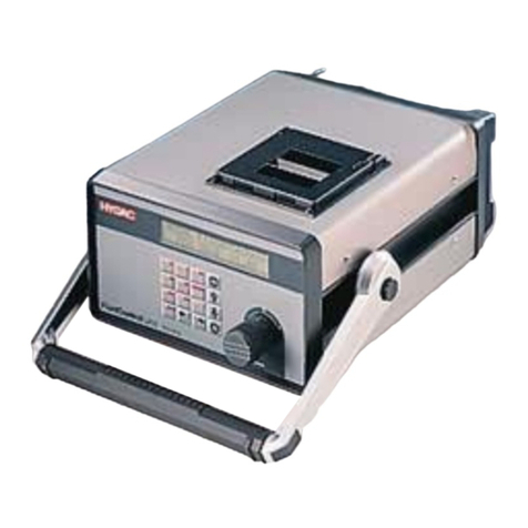
Hydac
Hydac FluidControl FCU 2000-1 Series Operating and maintenance instructions

Kanomax
Kanomax Anemomaster 6036 Operation manual
