EG&G ORTEC 553 Service manual
n
Model
553
Timing
Single-Channel
Analyzer
Operating
and
Service
Manual

Model
553
Tinning
Single-Channel
Analyzer
Operating
and
Service
Manual
This
manual
applies
to
instruments
marked
"Rev
18"
on
rear
panel
Printed
in
U.S.A.
ORTEC
Part
No.
733460
2661
0.2C
1087
standard
Warranty
for
EG&G
ORTEC
Nuclear
Electronic
Instruments
EG&G
ORTEC
warrants
that
the
items
will
be
delivered
free
from
defects
in
material
or
workmanship.
EG&G
ORTEC
makes
no
other
warranties,
express
or
implied,
and
specifically
NO
WARRANTY
OF
MERCHANTABILITY
OR
FITNESS
FOR
A
PARTICULAR
PURPOSE.
EG&G
ORTEC's
exclusive
liability
is
limited
to
repairing
or
replacing
at
EG&G
ORTEC's
option,
items
found
by
EG&G
ORTEC
to
be
defective
in
workmanship
or
materials
within
two
years
from
the
date
of
delivery.
EG&G
ORTEC's
liability
on
any
claim
of
any
kind,
including
negligence,
loss
or
damages
arising
out
of,
connected
with,
or
from
the
performance
or
breach
thereof,
or
from
the
manufacture,
sale,
delivery,
resale,
repair,
oruseof
any
item
or
services
covered
by
this
agree
ment
or
purchase
order,
shall
in
no
case
exceed
the
price
allocable
to
the
item
orservicefurnishedorany
part
thereof
that
gives
rise
to
the
claim.
In
the
event
EG&G
ORTEC
fails
to
manufacture
or
deliver
items
called
for
in
this
agreement
or
pur
chase
order,
EG&G
ORTEC's
exclusive
liability
and
buyer's
exclusive
remedy
shall
be
release
of
the
buyer
from
the
obliga
tion
to
pay
the
purchase
price.
In
no
event
shall
EG&G
ORTEC
be
liable
for
special
or
consequential
damages.
Quality
Control
Before
being
approved
for
shipment,
each
EG&G
ORTEO
nuclear
electronic
instrument
must
pass
a
stringent
set
of
quality
control
tests
designed
to
expose
any
flaws
in
materials
or
workmanship.
Permanent
records
of
these
tests
are
maintained
for
use
in
warrany
repair
and
as
a
source
of
statistical
information
for
design
improvements.
Repair
Service
If
it
becomes
necessary
to
return
this
instrument
for
repair,
it
is
essential
that
Customer
Services
be
contacted
in
advance
of
its
return
so
that
a
Return
Authorization
Number
can
be
assigned
to
the
unit.
Also,
EG&G
ORTEC
must
be
informed,
either
in
writing,
by
telephone
[(615)
482-4411
]
or
by
telex
(55-7450)
of
the
nature
of
the
fault
of
the
instrument
being
re
turned
and
of
the
model,
serial,
and
revision
("Rev"
on
rear
panel)
numbers.
Failure
to
do
so
may
cause
unnecessary
delays
in
getting
the
unit
repaired.
The
EG&G
ORTEC
standard
procedure
requires
that
instruments
returned
for
repair
pass
the
same
quality
control
tests
that
are
used
for
new-production
instruments.
Instruments
that
are
returned
should
be
packed
so
that
they
will
withstand
normal
transit
handling
and
must
be
shipped
PREPAID
via
Air
Parcel-
Post
or
United
Parcel
Service
to
the
nearest
EG&G
ORTEC
repair
center.
(In
the
case
where
the
instrument
did
not
function
upon
pur
chase,
EG&G
ORTEC
will
pay
shipment
costs
both
ways.)
The
address
label
and
the
package
should
include
the
Return
Authorization
Number
assigned.
Instruments
being
returned
that
are
damaged
in
transit
due
to
inadequate
packing
will
be
repaired
at
the
sender's
expense,
and
it
will
be
the
sender's
responsibility
to
make
claim
with
the
shipper.
Instruments
not
in
warranty
will
be
repaired
at
the
standard
charge
unless
they
have
been
grossly
misused
or
mishandled,
in
which
case
the
user
will
be
notified
prior
to
the
repair
being
done.
A
quotation
will
be
sent
with
the
notification.
Damage
in
Transit
Shipments
should
be
examined
immediately
upon
receipt
for
evidence
of
external
or
concealed
damage.
The
carrier
making
delivery
should
be
notified
immediately
of
any
such
damage,
since
the
carrier
is
normally
liable
for
damage
in
shipment.
Packing
materials,
waybills,
and
other
such
documentation
should
be
preserved
in
order
to
establish
claims.
After
such
notification
to
the
carrier,
please
notify
EG&G
ORTEC
of
the
circumstances
so
that
assistance
can
be
provided
in
making
damage
claims
and
in
providing
replacement
equipment
if
necessary.

CONTENTS
Page
WARRANTY
ii
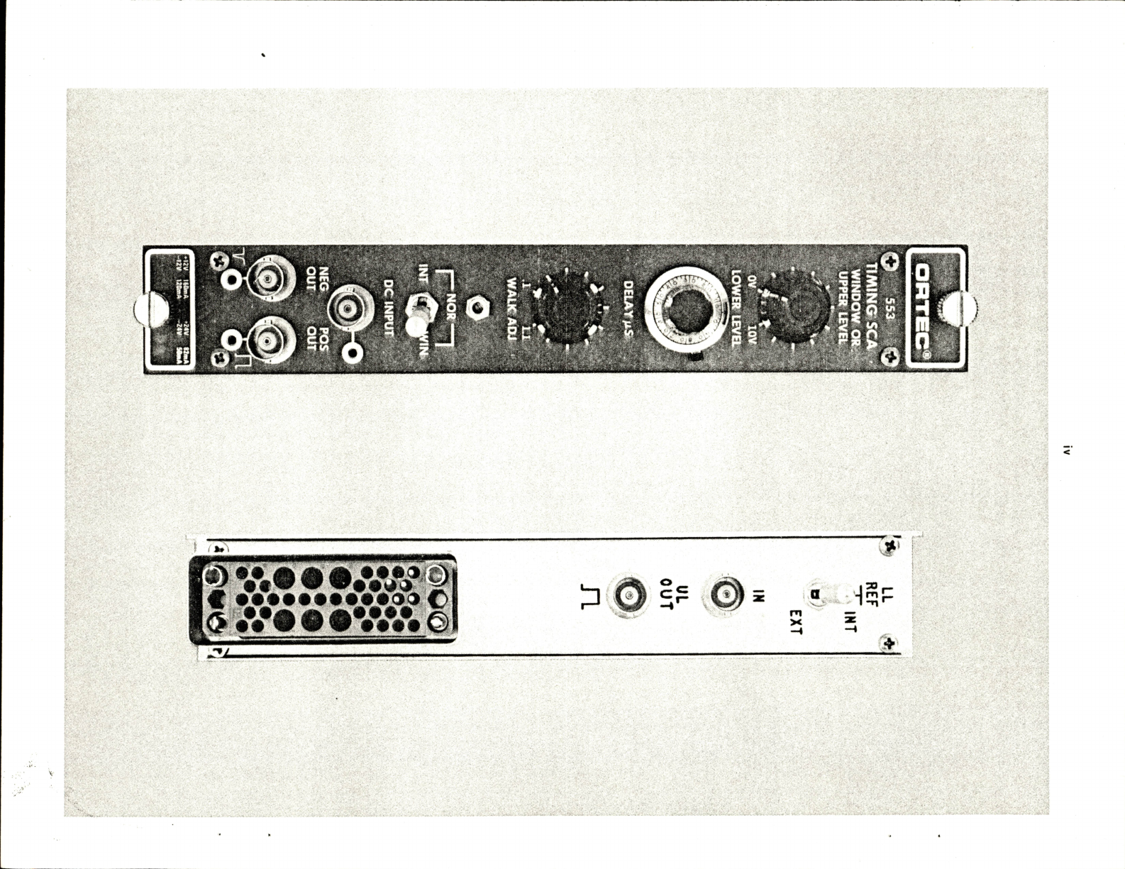
PHOTOGRAPHS
iv
1.
DESGRIPTiON
1
1.1.
Purpose
1
1.2.
Modes
of
Operation
1
1.3.
Output
Pulse
Timing
1
1.4.
Lower
Level
Reference
1
2.
SPECIFICATIONS
2
2.1.
Performance
2
2.2.
Controls
2
2.3.
Inputs
2
2.4.
Outputs
2
2.5.
Related
Equipment
2
2.6.
Electrical
and
Mecfianical
2
3.
INSTALLATION
3
3.1.
Connection
to
Power
3
3.2.
Connection
from
Linear
Amplifier
3
3.3.
Output
Connections
3
3.4.
Lower
Level
Reference
Input
3
4.
OPERATING
INSTRUCTIONS
4
5.
CIRCUIT
DESCRIPTION
5
5.1.
General
5
5.2.
Integrated
Circuits
5
5.3.
Lower
Level
Bias
5
5.4.
Upper
Level
Bias
6
5.5.
Input
Circuit
6
5.6.
Lower
Level
Discriminator
6
5.7.
Upper
Level
Discriminator
6
5.8.
Constant
Fraction
Circuit
6
5.9.
SCAGate
7
5.10.
Reset
Circuit
7
5.11.
Delay
Circuit
7
5.12.
DC
Power
7
6.
MAINTENANCE
AND
CALIBRATION
8
6.1.
General
8
6.2.
Calibration
8
6.3.
Factory
Repair
8
6.4.
Tabulated
Test
Point
Voltages
8
Block
Diagram
553-0101-B1
and
Schematic
553-0201-S1
ILLUSTRATIONS
Fig.
4.1.
Timing
Relationships
for
Input
and
Output
Pulses
4
Fig.
5.1.
Simplified
Block
Diagram
of
the
553
Timing
SCA
5
IV
's
-
n't-v
4.;
'
'«V
*
3
•
'
.v^'.
f'
'
'
,
}
'
'
■
>
'
^
„/
,
-••«'
fe
s-,'W
r
-,
.
f
^.
,
.
__
.
,
__
•«
^
'V-,
*
-
:
'-
»
%
y.>^-^.
.
;
..i
t
',f
^'.
^
,,
*
■'•*•
'
.
.
•*.
*.
.
, ,
"
,
,
,
;
.
,
'
.
■
'
,
.
..
,.
...1^
ISSsfU
.
-"-.1
iimm-mmy
LOWER-
LEVEL
DElAYjiS^V
,-—1,-
-
.1
'
Ll
WALK^AOL
.'.i^y,
^NOR—1^
INF
DC
INPUT
.
NEG
,.^
POS
OUT
^
sOUr
I
SSKSli^B&SE^
ilEB
LL
REF
INT
EXT
IN
UL
OUT
v4l'/
n
©g©
•52Sj
5''v*Si
wSMSyyyisy0Ws0SfiySiM&
:fcw,.
Ai

ORTEC
553
TIMING
SINGLE-CHANNEL
ANALYZER
1.
DESCRIPTION
1.1.
PURPOSE
The
ORTEC
553
Timing
Single-Channel
Analyzer
pro
vides
a
versatile
group
of
related
signal
derivation
func
tions.
It
can
be
used
as
either
a
single-channel
analyzer
or
as
an
Integral
discriminator.
The
principal
output,
furnished
as
both
a
NIM-standard
fast
negative
signal
and
a
NIM-standard
slow
positive
signal,
can
be
used
for
accurate
timing
information.
In
addition,
a
separate
NIM-
standard
slow
positive
output
is
furnished
separately
for
each
response
by
the
upper
level
discriminator
in
the
module.
The
output
signal
is
internally
generated
and
its
timing
relative
to
that
of
the
input
signal
is
derived
accurately,
using
a
time
recognition
technique
called
Constant-
Fraction
Discrimination.
This
technique
provides
unex
celled
timing
on
either
unipolar
or
bipolar
signals
which
displaces
<±3
ns
for
an
input
amplitude
variation
as
great
as
100:1.
This
eliminates
the
degradation
of
time
resolu
tion
for
varying
input
amplitudes
that
is
characteristic
of
leading-edge
time
recognition.
The
553
accepts
either
unipolar
or
bipolar
input
pulses
having
either
PC
or
delay-line
pulse-shaping
waveforms.
It
examines
the
amplitude
of
each
input
pulse
and
generates
appropriate
output
pulses
separately
for
SCA
and
ULD
responses.
The
SCA
output
is
delayed
from
the
time
of
recognition
(at
50%
of
full
amplitude
on
the
trailing
edge
of
the
input
positive
waveform).
The
delay
is
adjusted
on
the
front
panel
between
100
ns
and
1.1
ns
so
that
the
output
time
can
be
normalized
to
its
application.
The
instrument
is
designed
to
meet
the
recommended
interchangeability
standards
of
ERDA
Report
TID-20893
(Rev).
An
ORTEC
401/402
Series
Bin
and
Power
Supply
provides
all
the
necessary
power
through
the
rear
panel
power
connector.
All
signal
levels
and
impedances
are
compatible
with
other
ORTEC
NIM
modules.
1.2.
MODES
OF
OPERATION
The
553
has
a
front
panel
switch
that
selects
the
integral
mode
of
operation
or
either
of
two
types
of
differential
single-channel
analysis
modes.
For
Normal
operation,
each
of
the
discriminator
levels
is
adjusted
independ
ently
through
the
full
dynamic
range
of
0
to
10
V.
For
Window
operation,
the
range
of
the
lower
level
control
is
0
to
10
V
and
the
range
of
the
upper
level
(or
window)
control
is
the
adjusted
lower
level
plus
0
to
1
V.
Integral
Mode
Operation
In
the
integral
mode,
the
553
generates
an
output
through
both
the
Pos
Out
and
Neg
Out
connectors
on
the
front
panel
if
the
input
pulse
amplitude
exceeds
the
adjusted
lower
level
threshold;
the
range
is
0
to
10
V.
Normal
Mode
Operation
In
the
normal
mode,
the
553
generates
an
output
through
both
the
Pos
Out
and
Neg
Out
connectors
on
the
front
panel
if
the
input
pulse
amplitude
exceeds
the
adjusted
lower
level
but
does
not
exceed
the
adjusted
upper
level
threshold.
In
this
mode,
each
threshold
is
adjusted
independently
in
the
range
of
0
to
10
V,
and
the
upper
level
must
be
set
higher
than
the
lower
level
to
permit
the
SCA
outputs
to
be
generated.
Window
Mode
Operation
In
the
window
mode,
the
553
generates
an
output
through
both
the
Pos
Out
and
Neg
Out
connectors
on
the
front
panel
if
the
input
pulse
amplitude
exceeds
the
adjusted
lower
level
threshold,
but
by
an
amount
that
is
less
than
the
adjusted
window
width.
The
range
of
the
lower
level
control
is
0
to
10
V,
and
the
range
of
the
upper
level
control
is
0
to
1
V
above
the
lower
level.
This
mode
is
especially
adapted
to
high-
resolution
spectroscopy
because
the
very
narrow
win
dows
that
are
required
can
be
obtained
easily
and
reproducibly.
1.3.
OUTPUT
PULSE
TIMING
The
Pos
Out
and
Neg
Out
pulses
from
the
553
are
generated
at
a
delay
(with
internal
strobe)
following
the
precise
constant-fraction
time
recognition,
which
occurs
at
50%
of
the
peak
amplitude
on
the
trailing
edge
of
the
input
pulse.
The
delay
interval
is
adjustable
through
a
range
of
0.1
to
1.1
^iS.
The
front
panel
Delay
control
is
a
1-turn
potentiometer
that
is
marked
in
linear
increments
to
read
the
adjusted
delay
directly.
For
any
mode
of
operation,
a
signal
is
furnished
through
the
UL
Out
connector
on
the
rear
panel
when
the
upper
level
discriminator
is
triggered
on
the
leading
edge
of
the
input
signal.
Each
of
these
outputs
is
a
NIM-standard
positive
signal
that
can
be
used
for
any
desired
external
application.
1.4.
LOWER
LEVEL
REFERENCE
A
rear
panel
2-position
locking
toggle
switch
selects
either
the
front
panel
Lower
Level
control
or
the
voltage
signal
applied
through
the
rear
panel
LL
Ref
connector
as
the
reference
level
for
the
lower
level
discriminator.
This
permits
flexibility
in
operation,
where
an
external
reference
source
can
furnish
the
lower
level
threshold
from
a
stepped-
or
sliding-voltage
source
to
automati
cally
sweep
the
SCA
response
through
a
spectral
range
of
0
to
10
V.
The
selected
source
for
the
Lower
Level
Reference
is
effective
for
all
three
operating
modes.

2.
SPECIFICATIONS
2.1.
PERFORMANCE
Dynamic
Range
100:1.
Pulse-Pair
Resolving
Time
Output
pulse
width
plus
Delay
(as
selected
by
the
front
panel
Delay
control),
plus
100
ns
for
negative
NIM
output
or
plus
200
ns
for
positive
NIM
output.
Minimum
resolving
time
for
negative
output,
220
ns;
for
positive
output,
800
ns.
Threshold
Temperature
instability
<0.015%/°
C
of
full
scale,
0
to
50°C
using
a
NIM
class
A
power
supply
(referenced
to
-12
V).
Discriminator
Noniinearity
<±0.25%
of
full
scale
(inte
gral)
for
LL
discriminator.
Delay
Temperature
instability
<0.04%/°C
of
full
scale,
0
to
50°
C.
Delay
Noniinearity
<±2%.
Window
Width
Constancy
<0.1%
variation
of
full-scale
window
width
over
the
linear
0-
to
10-V
range.
Minimum
input
Threshold
50
mV
for
Lower
Level
dis
criminator.
Time
Shift
vs
Pulse
Height
(Walk)
Walk
(ns)
Dynamic
Range
10:1
50:1
100:1
System
System
A
B
±1.0
±2.5
±3.0
±2.0
±4.0
±8.0
System
A:
Using
an
ORTEC
460
Amplifier,
single
delay-l
ine
mode,
integrate
^0.1
ms
with
delay
line
1
mS-
System
B:
Using
an
ORTEC
471
or
472A
Amplifier,
unipolar
output
with
0.5
fiS
shaping
time,
input
from
ORTEC
419
Pulser.
2.2.
CONTROLS
Lower
Level
Front
panel
10-turn
potentiometer
adjust
able
from
0
to
10
V;
when
the
rear
panel
LL
Ref
mode
switch
is
set
on
Int,
determines
the
threshold
setting
for
the
Lower
Level
discriminator.
When
the
LL
Ref
mode
switch
on
the
rear
panel
is
in
the
Ext
position,
this
control
is
ineffective.
Window
or
Upper
Level
Front
panel
1-turn
potenti
ometer
determines
the
window
width
(0
to
+1
V)
in
the
Window
mode
or
the
Upper
Level
(0
to
+10
V)
threshold
in
the
Normal
mode.
This
control
is
disabled
in
the
Integral
mode.
Int/Nor/Win
Front
panel
3-position
locking
toggle
switch
selects
one
of
three
operating
modes.
Integral
LL
sets
a
single-discriminator
threshold
(0
to
+10
V)
and
UL
response
is
ignored
for
SCA
outputs.
Normal
UL
and
LL
are
independently
adjustable
lev
els
(0
to
+10
V);
differential
mode
operation.
Window
LL
sets
the
baseline
level
(0
to
+10
V)
and
UL
sets
the
window
width
(0
to
+1
V);
differential
mode
operation.
Delay
Front
panel
1-turn
potentiometer
for
continuous
adjustment
of
output
delay
over
a
0.1
to
1.1
fis
range.
Walk
Adjust
Front
panel
screwdriver
adjustment
for
precise
setting
of
walk
compensation.
LL
Ref
Mode
Rear
panel
two-position
locking
toggle
switch
selects
either
the
front
panel
LL
potentiometer
or
the
voltage
signal
applied
to
the
rear
panel
LL
Ref
Ext
connector
as
the
LL
discriminator
reference
threshold.
2.3.
INPUTS
Signal
Input
Front
panel
dc-coupled
BNC
connector
accepts
positive
unipolar
or
bipolar
signal,
0
to
+10
V
linear
range,
±12
V
maximum;
width,
^100
ns;
lOOOfl
input
impedance.
LL
Ref
Ext
When
the
rear
panel
LL
Ref
mode
switch
is
on
Ext,
the
rear
panel
LL
Ref
Ext
BNC
connector
accepts
the
Lower
Level
biasing
(an
input
of
0
to
-10
V
on
this
connector
corresponds
to
a
range
of
0
to
10
V
for
the
Lower
Level
discriminator
setting).
Input
protected
to
±24
V.
2.4.
OUTPUTS
Pos
Out
Front
panel
BNC
connector
provides
positive
NIM-standard
output,
nominally
+5
V;
<20
ns
rise
time,
500
ns
wide;
<10n
output
impedance.
Output
occurs
at
the
mid-point
of
the
linear
input
trailing
edge
plus
the
output
Delay
as
selected
by
the
front
panel
control.
Neg
Out
Front
panel
BNC
connector
provides
negative
NIM-standard
output,
nominally
-16
mA
(800
mV
on
50fi
load);
width,
<20
ns;
rise
time,
<5
ns.
Output
occurs
at
the
mid-point
of
the
linear
input
trailing
edge
plus
the
output
Delay
as
selected
by
the
front
panel
control.
UL
Out
Rear
panel
BNC
connector
provides
NIM-
standard
output,
nominally
+5
V,
500
ns
wide;
<10n
output
impedance.
Output
occurs
as
leading
edge
of
linear
input
crosses
the
UL
threshold.
2.5.
RELATED
EQUIPMENT
The
553
is
compatible
with
all
ORTEC
amplifiers
and
other
amplifiers
having
a
0-
to
10-V
positive,
linear
output
range.
2.6.
ELECTRICAL
AND
MECHANICAL
Power
Required
+24
V,
82
mA;
+12
V,
160
mA;
-24
V,
50
mA;
-12
V,
120
mA.
Dimensions
NIM-standard
single-width
module
(1.35
by
8.714
in.)
per
TID-20893
(Rev).

3.
INSTALLATION
The
553
must
be
used
in
conjunction
with
an
ORTEC
401/402
Series
Bin
and
Power
Supply
or
equivalent,
which
is
intended
for
rack
mounting.
Therefore
if
vacuum
tube
equipment
or
any
other
source
of
heat
is
operating
in
the
same
rack,
there
must
be
sufficient
cooling
air
circulating
to
prevent
any
localized
heating
of
the
transistorized
and
integrated
circuits
used through
out
the
553.
The
temperature
of
equipment
mounted
in
racks
can
easily
exceed
the
maximum
unless
precau
tions
are
taken;
the
553
should
not
be
subjected
to
temperatures
in
excess
of
120°F
(50°C).
3.1.
CONNECTION
TO
POWER
Turn
off
the
Bin
Power
Supply
when
inserting
or
remov
ing
modules.
The
ORTEC
NIM
modules
are
designed
so
that
it
is
not
possible
to
overload
a
properly
operating
power
supply
with
a
full
complement
of
modules
in
the
bin.
Since,
however,
this
may
not
be
true
when
the
bin
contains
modules
other
than
those
of
ORTEC
design,
power
supply
voltages
should
be
checked
after
the
modules
have
been
inserted.
The
401/402
has
test
points
on
the
power
supply
control
panel
to
monitor
dc
voltages.
When
using
the
553
outside
the
401/402
Bin
and
Power
Supply,
be
sure
that
the
power
extension
cable
that
is
used
properly
accounts
for
the
power
supply
grounding
circuits
that
are
provided
according
to
the
recommended
ERDA
standards
outlined
in
TID-20893
(Rev).
Both
high-
quality
and
power-return
ground
connections
are
pro
vided
to
ensure
proper
reference
voltage
feedback
into
the
power
supply,
and
these
must
be
preserved
in
remote
cable
installations.
Be
careful
also
to
avoid
ground
loops
when
the
module
is
operated
outside
the
bin.
3.2.
CONNECTION
FROM
LINEAR
AMPLIFIER
The
553
can
be
used
for
the
analog
signals
that
are
furnished
from
a
linear
amplifier.
The
BNC
on
the
front
panel
accepts
input
signals
through
a
dc-coupled
path.
The
input
circuit
accepts
positive
unipolar
pulses
or
bipolar
pulses
(the
positive
lobe
will
be
analyzed)
into
an
input
impedance
of
^lOOOfl.
When
long
cables
(more
than
about
4
ft)
are
used
to
connect
the
amplifier
output
to
the
553
input,
cable
termination
may
be
necessary
in
order
to
prevent
reflections;
match
the
cable
impedance
with
a
terminator
at
the
553
input
in
such
cases.
3.3.
OUTPUT
CONNECTIONS
The
logic
output
pulses
that
are
generated
when
input
pulses
satisfy
the
amplitude
and
logic
requirements
of
the
553
are
available
through
both
front
and
rear
panel
BNC
connectors.
NIM-standard
fast
negative
signals
are
available
through
the
front
panel
Neg
Out
BNC.
NIM-
standard
slow
positive
signals
are
available
through
the
front
panel
Pos
Out
connector.
When
the
553
is
set
for
either
differential
single-channel
mode
(normal
or
window),
the
logic
output
pulse
means
that
an
input
pulse
amplitude
is
sufficient
to
trigger
the
lower
level
discriminator
without
also
triggering
the
upper
level
discriminator.
When
the
553
is
set
for
its
integral
mode
of
operation,
the
logic
output
means
that
an
input
pulse
amplitude
is
sufficient
to
trigger
the
lower
level
discriminator;
triggering
of
the
upper
level
discrimi
nator
does
not
affect
the
output.
The
time
when
both
SCA
logic
output
signals
are
made
available
is
the
result
of
an
internal
strobe.
The
strobe
originates
from
the
constant-fraction
trigger,
at
50%
amplitude
on
the
decay
of
the
positive
input
pulse.
This
strobes
a
delay
circuit,
with
the
delay
interval
adjusted
with
a
front
panel
control
between
0.1
and
1.1
^s,
and
the
outputs
occur
at
the
end
of
the
delay
interval.
A
logic
output
is
available
through
the
rear
panel
to
indicate
when,
on
the
leading
edge
of
an
input
pulse,
the
UL
discriminator
is
triggered.
These
responses
can
be
used
to
monitor
the
discriminator
levels
during
adjust
ment,
to
be
counted
in
external
sealers,
to
provide
subgroup
routing
in
a
multichannel
analyzer,
or
for
any
other
applications
as
desired.
Each
logic
output
for
UL
Out
is
a
NIM-standard
slow
positive
pulse
that
is
com
patible
with
all
ORTEC
counters,
counting
rate
meters,
and
other
instruments.
The
output
impedance
through
each
output
path
is
sufficiently
low
to
drive
as
many
as
ten
paralleled
lOOOH
inputs.
3.4.
LOWER
LEVEL
REFERENCE
INPUT
If
the
LL
Ref
toggle
switch
on
the
rear
panel
of
the
553
is
set
at
Ext,
the
reference
level
for
the
lower
level
discrimi
nator
must
be
furnished
through
the
adjacent
LL
Ref
In
BNC
connector;
the
10-turn
Lower
Level
control
on
the
front
panel
is
disconnected.
An
input
of
0
to
-10
V
through
this
connector
corresponds
directly
to
a
range
of
0
to
+10
V
for
the
lower
level
discriminator
threshold.
If
an
input
is
connected
to
the
LL
Ref
connector
and
the
switch
selects
Int,
the
signal
through
the
connector
is
ignored.

4.
OPERATING
INSTRUCTIONS
After
the
553
has
been
connected
into
a
system
accord
ing
to
the
installation
information
in
Section
3,
the
operating
mode
can
be
selected
and
the
discriminator
thresholds
can
be
adjusted
as
required
for
each
appli
cation.
Figure
4.1
illustrates
the
timing
relationships
that
will
be
effective
in
the
553
for
each
of
three
possible
input
pulse
amplitudes.
The
first
two
pulses
exceed
the
lower
level
threshold
without
also
exceeding
the
upper
level,
and
the
third
pulse
exceeds
both
threshold
levels.
Superimposed
in
each
of
these
input
pulses
in
Fig.
4.1
is
an
internally-
generated
signal
that
rises
to
50%
of
the
input
peak
amplitude
and
is
stretched
at
that
level.
When
the
input
pulse
decays
through
the
50%
level,
the
CF
discriminator
resets
and,
when
delayed
by
a
fixed
interval,
triggers
the
SCA
outputs
if
the
analysis
criteria
have
been
satisfied.
The
delay
interval
can
be
adjusted
within
the
range
of
0.1
to
1.1
(us
using
a
front
panel
control.
If
the
pulses
of
Fig.
4.1
were
furnished
to
a
553
that
was
set
for
its
Normal
or
Window
(differential)
mode,
time-significant
SCA
output
pulses
would
be
generated
for
each
of
the
first
two
input
pulses
but
none
would
be
generated
for
the
third
be
cause
its
amplitude
was
greater
than
the
upper
level
threshold.
If
the
pulses
were
furnished
to
a
553
that
was
set
for
its
Integral
mode,
a
time-significant
output
pulse
pair
would
be
generated
for
each
of
the
three
input
pulses.
In
either
mode
of
operation,
a
ULD
output
will
result
when
the
corresponding
discriminator
threshold
is
exceeded
by
the
input
pulse
amplitude.
The
adjusted
lower
level
threshold
is
furnished
either
from
the
front
panel
Lower
Level
control
or
from
an
external
source
through
the
rear
panel
LL
Ref
connector;
the
alternate
selection
is
made
with
the
rear
panel
LL
Ref
toggle
switch
-
either
Int
for
the
front
panel
control
or
Ext
for
the
rear
panel
8NC.
In
either
case,
the
range
is
from
0
to
+10
V,
measured
from
chassis
ground,
of
the
input
signal.
The
adjusted
upper
level
threshold
is
determined
by
the
setting
of
the
front
panel
Upper
Level
or
Window
control
and
by
the
front
panel
mode
selector
toggle
switch.
When
the
switch
is
set
at
either
Int
or
Nor,
the
range
of
the
variable
control
is
from
0
to
+10
V,
measured
from
chassis
ground.
When
the
toggle
switch
is
set
at
Win,
the
range
of
the
variable
control
is
0
to
+1
V,
measured
above
the
adjusted
lower
level
threshold.
For
optimum
time-significant
SCA
output
timing,
the
front
panel
Walk
Adj
must
be
trimmed
to
the
combined
effects
of
the
input
shaping
and
its
time
constants
and
of
the
expected
dynamic
range
of
operation.
Using
a
dupli
cate
of
the
minimum
and
maximum
amplitudes
for
shaped
input
pulses,
set
the
control
to
provide
the
minimum
walk
(variation
of
time
of
occurrence
vs
input
amplitude).
ULD
CF
TRIGGER
Delay
adjusted
in
range
of
0.1
to
1.1
jjs
—•
(DIFF)
SCA
POS
OUT
(DIFF)
SCA
NEC
OUT
(INT)
SCA
POS
OUT
rL_
(INT)
SCA
NEG
OUT
Y
Hh
-Ih
Hh
■ih
n
Fig.
4.1.
Timing
Relationships
for
Input
and
Output
Pulses.

5.
CIRCUIT
DESCRIPTION
5.1.
GENERAL
Refer
to
schematic
diagram
553-0201-S1
included
at
the
back
of
the
manual.
Figure
5.1
is
a
simplified
block
diagram
of
the
553
Timing
SCA.
It
shows
that
each
input
pulse
is
furnished
to
three
internal
discriminators
and
also
through
an
attenuate
and
peak
stretch
circuit.
The
three
discriminators
are
UL
(upper
level),
LL
(lower
level),
and
CP
(constant
frac
tion).
Each
discriminator
independently
triggers
a
re
sponse
when
the
amplitude
of
its
noninverted
input
exceeds
the
amplitude
of
its
inverted
input.
The
response
of
the
UL
and
LL
discriminators
is
latched
until
an
internal
reset
occurs.
The
CP
discriminator
is
reset
again
when
the
input
conditions
are
reversed.
Reference
levels
for
the
UL
and
LL
discriminators
are
set
independently
for
either
Integral
or
Normal
mode
opera
tion.
For
Window
operation,
the
threshold
for
the
UL
discriminator
is
based
on
the
LL
setting
instead
of
ground.
The
CP
discriminator
is
triggered
at
the
onset
of
each
input
pulse,
whether
its
amplitude
is
sufficient
to
trigger
either
of
the
other
two
discriminators
or
not.
Then
the
CP
discriminator
is
reset
when
the
amplitude
of
the
input
pulse
decays
through
its
50%
level
because
the
attenuate
and
peak
stretch
circuit
has
generated
and
maintained
this
50%
level
by
that
time
and
furnished
it
as
the
discriminator
reference
level.
The
SCA
gate
is
triggered
when
the
CP
discriminator
is
reset
if,
at
that
time,
the
LL
discriminator
has
been
triggered
and
the
UL
discriminator
either
has
not
been
triggered
(for
differential
operation)
or
is
ignored
(for
integral
operation).
Thus
the
gate
responds
to
both
logical
conditions
and
input-pulse
time
significance.
If
the
SCA
gate
responds,
it
strobes
a
delay
circuit
that
then
generates
the
SCA
outputs
at
the
end
of
the
delay
interval.
5.2.
INTEGRATED
CIRCUITS
The
nomenclature
used
to
identify
integrated
circuit
packages
in
this
manual
is
defined
below
for
the
example
IC5(4)
where
IC
=
integrated
circuit,
5
=
reference
designation,
(4)
=
pin
number.
Any
portion
of
an
IC
package
can
be
designated
by
its
output
pin
number:
in
this
example,
the
portion
of
IC5
that
includes
pin
4
as
an
output
is
identified
uniquely.
5.3.
LOWER
LEVEL
BIAS
The
threshold
for
the
lower
level
discriminator
is
ad
justed
with
the
front
panel
Lower
Level
control,
R43,
or
is
OUTPUT
T
Int
GENERATOR
UL
DISC
Nor/Win
DC
In
Int/Nor
LL
DISC
DELAY
OUTPUT
GENERATOR
CF
DISC
ATTENUATE
and
PEAK
STRETCH
CURRENT
SWITCH
UL
Out
-0
-0
Pos
Out
-0
Neg
Out
Fig.
5.1.
Simplified
Block
Diagram
of
tfie
553
Timing
SCA.

furnished
as
a
dc
level
through
CN3
on
the
rear
panel.
Switch
84
on
the
rear
panel
selects
which
of
these
sources
is
effective
for
bias
control.
For
the
internal
bias
circuit,
R47
is
a
potentiometer
mounted
on
the
printed
circuit
that
adjusts
the
minimum
level
for
the
front
panel
control.
The
actual
range
of
R43
is,
then,
from
a
few
millivolts
to
about
—5
V.
The
adjusted
level
is
buffered
through
IC2(7)
and
inverted
through
operational
amplifier
IC2{1),
with
a
gain
of
unity,
and
furnished
to
the
inverting
input
of
IC4,
the
lower
level
discriminator.
For
the
external
bias
circuit,
a
dc
level
between
0
and
-10
V
can
be
furnished
through
CN3
and
divided
by
R44
and
R45.
The
result
that
is
selected
with
switch
84
is
then
furnished
through
the
same
buffering
and
coupling
network
to
the
lower
level
discriminator.
5.4.
UPPER
LEVEL
BIAS
The
threshold
for
the
upper
level
discriminator
is
ad
justed
with
the
front
panel
Window
or
Upper
Level
control,
R38.
The
range
for
this
control
is
0
to
-5
V.
The
adjusted
level
is
buffered
through
IC1(7)
and
furnished
through
either
R55
or
R52,
through
operational
amplifier
IC1(1),
and
to
the
inverting
input
of
upper
level
discrimi
nator
IC3.
When
switch
81
is
set
at
either
Integrate
or
Normal,
the
gain
of
IC1{1)
for
this
adjusted
bias
signal
is
1.0;
when
the
switch
selects
Window,
the
gain
is
reduced
to
0.1
and
the
effective
range
of
the
Window
control
is
thus
reduced
by
a
factor
of
10.
Also,
when
the
switch
selects
Window,
the
level
that
is
furnished
from
IC2(7)
for
the
lower
level
discriminator
is
also
furnished
through
R50
and
IC1(1).
Thus
the
adjusted
lower
level
becomes,
effectively,
the
base
above
which
the
upper
level
is
added,
and
the
result
is
a
window
of
0
to
1
V
between
the
lower
level
and
upper
level
thresholds
(referred
to
the
input
pulse
amplitude).
The
gain
for
the
level
from
IC2(7)
through
IC1(1)
is
unity.
5.5.
INPUT
CIRCUIT
The
analog
input
signal
is
furnished
through
CN2
on
the
front
panel.
The
signal
is
then
furnished
to
dividers
R3-
R4
and
R147-R148,
and
50%
of
the
input
amplitude
is
applied
to
the
noninverting
inputs
of
both
the
UL
and
LL
discriminators,
IC3
and
104.
The
input
range
of
0
to
+10
V,
divided
by
two
for
an
effective
range
of
0
to
+5
V
at
the
discriminator
inputs,
is
directly
equivalent
to
the
range
of
threshold
levels
described
in
8ections
5.2
and
5.3.
The
input
signal,
through
the
front
panel
dc-coupled
circuit,
can
be
monitored
at
test
point
TP1
on
the
front
panel.
5.6.
LOWER
LEVEL
DISCRIMINATOR
Integrated
circuit
package
104
is
the
lower
level
discrimi
nator.
As
long
as
the
input
level
at
its
pin
3
does
not
exceed
the
level
at
pin
4,
the
output
at
its
pin
9
is
high.
When
the
amplitude
of
the
input
signal,
at
pin
3,
in
creases
above
the
threshold
level
at
pin
4,
104
triggers
and
reverses
the
levels
at
its
pins
9
and
11.
When
104(11)
goes
high,
106(13)
goes
low
and
latches
104(11)
in
the
high
state
until
a
reset
is
furnished
from
107(6).
The
reset
will
be
furnished
when
the
discriminator
returns
to
quies
cent
and
the
OF
discriminator
is
also
reset;
these
condi
tions
occur
on
the
trailing
edge
of
the
input
pulse.
Until
latch
106(13)
and
104(11)
is
reset,
the
high
level
to
pin
2
of
80A
gate
107(12)
arms
the
gate
to
permit
response
if
its
pins
1
and
13
go
high.
8ee
8ection
5.9,
80A
Gate.
5.7.
UPPER
LEVEL
DISCRIMINATOR
Integrated
circuit
package
103
is
the
upper
level
discrim
inator.
It
is
identical
to
104,
discussed
in
8ection
5.6,
except
that
its
output
at
pin
9
is
not
used.
If
the
amplitude
at
pin
3
increases
above
the
threshold
level
at
pin
4,
103
triggers
and
switches
the
output
at
103(11)
to
its
high
state.
This
output
at
pin
11
latches
through
106(10)
until
a
reset
is
furnished
from
107(6).
The
reset
will
be
furnished
when
both
the
lower
level
and
OF
discriminators
have
been
reset,
as
discussed
in
8ection
5.6.
At
the
trigger
time
on
the
leading
edge
of
the
input
signal,
when
103(11)
goes
high,
an
output
through
0N4,
the
UL
Out
connector,
is
generated
through
108(1),
022,
023,
and
024.
The
positive
output
pulse
has
a
width
of
about
500
ns.
If
switch
81
is
set
at
Int,
the
output
of
gate
107(8)
will
remain
high
whether
the
upper
level
discriminator
is
triggered
or
not.
But
if
the
switch
selects
either
Normal
or
Window
(for
differential
single-channel
operation),
a
response
in
103
will
furnish
a
low
signal
from
107(8)
to
inhibit
a
response
in
107(12)
and
prevent
an
80A
output
signal
from
being
generated.
5.8.
CONSTANT
FRACTION
CIRCUIT
The
input
signal
is
furnished
through
R2
into
a
peak
detect
circuit,
formed
by
Q1
through
Q5
and
O10.
During
the
rise
time
of
the
input
pulse,
the
capacitor
is
charged.
The
reverse
current
path
is
cut
off,
so
the
peak
amplitude
of
the
input
pulse
remains
on
O10
until
it
is
discharged
at
a
later
time.
The
peak
amplitude
of
the
input
pulse
is
furnished
through
a
unity-gain
buffer
amplifier,
Q8,
Q9,
and Q10.
The
front
panel
Walk
Adj
control,
R36,
provides
a
fine
adjustment
of
the
offset
of
this
amplifier
and
is
adjusted
for
its
dynamic
function
to
minimize
walk
in
the
time-
significant
output
pulses.
The
output
of
the
buffer
ampli
fier
is
furnished
through
R33
and
R31,
a
divide-by-4
attenuator.
From
this
circuit,
25%
of
the
peak
amplitude
of
the
signal
input
pulse
is
furnished
to
the
inverting
input
of
105.
Integrated
circuit
ICS
is
the
OF
discriminator.
The
inputs
at
its
pins
3
and
4
are
indicated
in
Fig.
4.1.
During
operation,
the
ICS
package
is
triggered
at
the
beginning
of
each
input
pulse,
as
soon
as
the
S0%
level
at
pin
4
exceeds
the
2S%
level
at
pin
3
by
just
a
few
millivolts.
Then,
during
decay
of
the
input
pulse,
the
level
at
pin
4
drops
down
through
the
level
at
pin
3
at
S0%
of
the
peak
amplitude,
which
is
a
dependable
and
precise
time
in
a
shaped
linear
pulse,
and
ICS
is
reset.
At
reset,
ICS(9)
goes
high
to
drive
pin
9
of
ICS
low
and
to
switch
IC6(1)
from
low
to
high.
R77
and
C34
provide
a
slight
delay
before
IC6(1)
reaches
a
high
level
and,
during
this
short
interval,
IC8(10)
goes
high.
The
level
at
IC8(10)
Is
one
of
the
three
inputs
to
SCA
Gate
IC7(12).
The
CF
discriminator
is
triggered
and
then
reset
during
each
input
pulse,
including
noise
pulses.
The
only
input
pulses
that
will
use
the
time-significant
CF
reset
are
those
that
also
trigger
the
LL
discriminator.
5.9.
SCA
GATE
Integrated
circuit
IC7(12)
is
the
SCA
Gate.
When
all
three
of
its
inputs
are
high,
the
output
switches
low
and
this
starts
generation
of
an
output
through
the
Pos
Out
and
the
Neg
Out
connectors.
The
signal
at
107(13)
is
high
unless
the
upper
level
discriminator
has
been
triggered
and
switch
81
is
set
at
either
Nor
or
Win
(the
differential
mode
of
operation).
A
response
by
the
UL
discriminator,
with
differential
oper
ation,
will
inhibit
a
response
in
IC7(12).
The
signal
at
IC7(2)
is
high
from
the
time
the
LL
discrim
inator
is
triggered
until
an
internal
reset
is
generated
by
IC7(6),
and
this
will
not
occur
before
the
reset
of
the
CF
discriminator.
Thus
a
response
by
the
LL
discriminator
is
a
prerequisite
to
enable
gate
IC7(12).
The
signal
at
IC7(1)
is
furnished
from
IC8(10)
when
the
CF
discriminator
is
reset
(see
Section
5.8).
Thus,
for
the
short
duration
of
the
signal
high
at
IC7(1),
and
if
the
single-channel
criteria
have
been
met
by
signals
at
IC7(2)
and
IC7(13),
then
IC7(12)
will
go
low.
5.10.
RESET
CIRCUIT
An
internal
reset
circuit
is
furnished
from
IC7(6),
going
low
when
all
three
inputs
are
high.
When
IC7(6)
goes
low,
it
resets
the
latch
for
the
LL
discriminator
through
IC6(13):
it
resets
the
latch
for
the
UL
discriminator
(if
it
has
been
triggered)
through
IC6(10);
and
it
turns
on
Q11
to
quickly
discharge
the
storage
capacitor
CIO
in
the
peak
detect
circuit.
At
the
start
of
an
input
signal,
at
the
CF
trigger
response,
the
input
of
IC7(6)
at
pin
3
goes
low
and
remains
low
until
just
after
the
CF
discriminator
is
reset
[the
signal
from
IC6(1),
R77,
and
C34].
The
signal
at
pin
4
goes
high
at
the
LL
discriminator
trigger
time
and
is
latched
high
through
IC4(11)
until
internal
reset
has
occurred.
The
third
input
to
IC7(6)
is
furnished
from
the
comple
mentary
output
of
IC4(9)
and
this
goes
high
when
IC4
is
reset.
The
IC4
reset
occurs
when
the
input
signal
ampli
tude
decays
back
through
the
adjusted
LL
threshold.
From
a
timing
point
of
view,
the
LL
trigger
and
reset
must
have
both
occurred
and
the
CF
discriminator
must
have
been
reset
before
all
three
inputs
to
IC7(6)
can
be
high
simultaneously.
Either
the
CF
or
the
LL
reset
can
occur
before
the
other,
but
the
reset
trigger
depends
on
both
events
having
occurred.
The
duration
of
the
low
signal
from
IC7(6)
is
the
propagation
time
for
the
reset
of
latch
IC6(13)
and
IC4(11).
Since
the
reset
circuit
is
dependent
upon
the
lower
level
discriminator,
and
since
in
the
Normal
and
Integral
modes
it
is
possible
to
adjust
the
upper
level
threshold
for
a
response
at
less
than
the
lower
level
threshold,
this
combination
could
result
in
a
single
response
through
the
UL
Out
without
its
latch
being
reset
until
the
lower
level
threshold
is
also
exceeded
by
an
input.
This
condi
tion
will
not
exist
in
the
Window
mode,
since
it
is
not
possible
to
set
the
UL
below
the
LL
level.
5.11.
DELAY
CIRCUIT
When
IC7(12)
goes
low
(Section
5.9),
IC8(13)
goes
high
and
triggers
the
delay
circuit.
The
delay
circuit
includes
Q15, Q16, Q19,
Q20,
and
Q21
and
their
associated
circuitry.
When
the
trigger
is
furnished
to
Q15,
Q16
is
cut
off
and
held
in
the
off
state
by
the
signal
from
Q21
and
C45.
Q16
then
returns
to
its
normally
conducting
condi
tion
when
C45
is
recharged
by
current
through
Q19.
When
Q16
is
turned
on
again,
the
negative
output
transi
tion
triggers
the
SCA
outputs.
Potentiometer
R115,
the
Delay
control
on
the
front
panel,
combines
with
the
Q19E
level
to
determine
the
current
rate
that
will
recharge
045
and
thus
determine
the
recovery
time
for
the
delay
circuit.
Pin
9
of
109
is
held
high
and
at
the
start
of
the
delay
interval,
pin
10
of
109
goes
high
and
this
propagates
through
109(11)
and
109(6)
to
furnish
a
low
to
pin
3
of
1010(1),
arming
this
gate.
At
the
negative
transition
from
Q160,
109(8)
switches
high
so
109(3)
goes
low
and
triggers
the
current
switch
Q13
and
Q14
for
the
Neg
Out
signal;
the
negative
transition
also
triggers
1010(1)
to
furnish
a
negative
pulse
through
1010(4)
and
start
the
generation
of
the
Pos
Out
signal.
Both
of
these
triggers
are
terminated
by
the
fast
differentiation
of
R89
and
038.
The
base
level
for
016
is
very
sensitive,
so
a
temperature
compensating
network
is
connected
between
this
point
and
ground.
5.12.
DC
POWER
Input
power
from
the
bin
and
power
supply
is
accepted
through
the
module
connector
on
the
rear
panel.
The
553
operates
on
82
mA
through
the
-1-24
V
circuit,
160
mA
through
the
-1-12
V
source,
50
mA
from
-24
V,
and
120
mA
from
-12
V.
Internally,
the
+12
V
source
is
furnished
to
a
circuit
that
uses
Q32
and
Q33
to
generate
a
regulated
+5
V
level.
The
+5
V
level
is
used
in
the
integrated
circuit
packages
that
are
in
the
553
circuits.
6.
MAINTENANCE
AND
CALIBRATION
6.1.
GENERAL
The
basic
performance
of
the
553
Timing
SCA
can
be
inferred
from
its
operating
responses.
If
the
unit
faiis
to
respond
properly
at
any
time,
use
the
information
in
Section
5
to
identify
the
probable
fault.
The
block
dia
gram
of
Fig.
5.1
and
schematic
553-0201-31
identify
all
of
the
circuits
in
the
instrument.
6.2.
CALIBRATION
There
is
a
provision
for
the
calibration
of
the
CF
refer
ence
circuit.
Potentiometer
R17,
mounted
on
the
printed
circuit,
permits
this
calibration.
Use
the
follov/ing
proce-
cure:
1.
Connect
a
jumper
between
Q4C
and
R28,
as
indi
cated
on
schematic
553-0201-81.
This
ties
the
input
to
the
buffer
amplifier
at
ground.
2.
Set
potentiorheter
R17
fully
counterclockwise,
as
viewed
from
the
top.
3.
Measure
the
output
of
the
buffer
amplifier
at
Q9C.
Adjust
front
panel
Walk
Adj
(R36)
as
necessary
to
obtain
0
V
±
1
mV.
4.
Remove
the
jumper
between
Q4G
and
R28.
5.
With
no
input
signals,
adjust
R17
as
necessary
to
obtain
0
V
again
at
the
buffer
amplifier
output,
Q9C.
6.3.
FACTORY
REPAIR
This
instrument
can
be
returned
to
the
ORTEG
factory
for
service
and
repair
at
a
nominal
cost.
Our
standard
procedure
for
repair
ensures
the
same
quality
control
and
checkout
that
are
used
for
a
new
instrument.
Always
contact
the
Customer
Service
Department
at
ORTEG,
(615)
482-4411,
before
sending
in
an
instrument
for
repair
to
obtain
shipping
instructions
and
so
that
the
required
Return
Authorization
Number
can
be
assigned
to
the
unit.
Write
this
number
on
the
address
label
and
on
the
package
to
ensure
prompt
attention
when
the
ship
ment
reaches
the
ORTEG
factory.
6.4.
TABULATED
TEST
POINT
VOLTAGES
The
following
voltages
are
intended
to
indicate
the
typical
dc
voltages
that
can
be
measured
on
the
printed
circuit.
In
some
cases
the
circuit
will
perform
satisfac
torily
even
though,
due
to
component
tolerances,
some
voltages
may
differ
slightly
from
those
that
are
tabulated
in
Table
6.1.
Therefore
the
voltages
that
are
listed
should
not
be
considered
absolute,
but
rather
are
intended
as
an
aid
in
troubleshooting.
All
voltages
were
measured
with
no
input
signal
and
with
the
front
panel
switch
set
for
Integral
mode.
Table
6.1.
Typical
dc
Voltages.
Location
Voltage
Location
Voltage
Location
Voltage
R38-R39
junction
-5.02
Q17B
1.0
104(6)
-12.
R43-R42
junction
-5.02
Q17E
0.8
104(9)
4.1
QiE
0.6
Q18B
0.1
104(11)
0.1
Q2E
0.6
Q20B
5.3
104(14)
5.0
Q2C
20.5
Q21E
12.6
105(3)
0
Q5A(S)
1.2
Q22B
0.8
105(4)
0
Q5B(S)
1.2
Q22C
0.1
105(6)
-5.7
Q6E
-0.5
G23C
12.
105(11)
12.
Q7B
-0.5
Q23E
0.2
106(9)
4.1
Q7E
-1.2
Q25B
0.8
106(10)
4.1
Q8B
16.3
Q25C
0.1
106(13)
4.1
Q9B
15.0
Q26C
12.
107(8)
4.1
Q10A(G)
0
Q26E
0.2
107(12)
4.1
QIOA(S)
1.2
Q28B
0.8
108(1)
5.3
QIOB(G)
0
Q20E
0.1
108(2)
0.2
Q11B
-1.3
029E
0.1
108(4)
5.3
Q12B
-1
.0
Q29C
12.
108(10)
0.1
Q12E
-1.7
0328
5.1
108(13)
0.1
Q13B
-0.4
033B
5.8
108(14)
5.0
Q14B
-1.3
IC3{1)
12.
109(3)
4.
1
Q14E
-1.2
IC3(3)
0
109(6)
4.
1
Q14C
0
IC3(6)
-12.
109(8)
4.0
Q15B
-1.5
IC3(11)
0.1
109(11)
0.4
Q15C
12.
IC3(14)
5.0
1010(1)
0.1
Q16B
-0.5
IC4(1|
12.
1010(4)
4.1
Q16E
-1.1
IC4(3)
0
D8A
2.6
Q16C
0.6

BIN/MODULE
CONNECTOR
PIN
ASSIGNMENTS
FOR
AEC
STANDARD
NUCLEAR
INSTRUMENT
MODULES
PER
TID-20893
(Rev
4)
(adopted
by
DOE)
Pin
Function
Pin
Function
1
+3
volts
23
Reserved
2
-3
volts
24
Reserved
3
Spare
Bus
25
Reserved
4
Reserved
Bus
26
Spare
5
Coaxial
27
Spare
6
Coaxial
*28
+24
volts
7
Coaxial
*29
-24
volts
8
200
volts
do
30
Spare
Bus
9
Spare
31
Spare
-10
+6
volts
32
Spare
'11
-6
volts
*33
117
volts
ac
(Hot)
12
Reserved
Bus
*34
Power
Return
Ground
13
Spare
**35
Reset
(Sealer)
14
Spare
**36
Gate
15
Reserved
**37
Reset
(Auxiliary)
•16
+12
volts
38
Coaxial
*17
-12
volts
39
Coaxial
18
Spare
Bus
40
Coaxial
19
Reserved
Bus
*41
117
volts
ac
(Neut.)
20
Spare
*42
High
Quality
Ground
21
Spare
G
Ground
Guide
Pin
22
Reserved
Pins
marked
{*)
are
installed
and
wired
in
EG&G
ORTEC's
4001
A,
4001B,
4001C,
401
A,
and
4018
Modular
System
Bins.
Pins
marked
(*)
and
(")
are
installed
in
EG&G
ORTEC-HEP-M250/N
and
M350/N
NIMBINS.
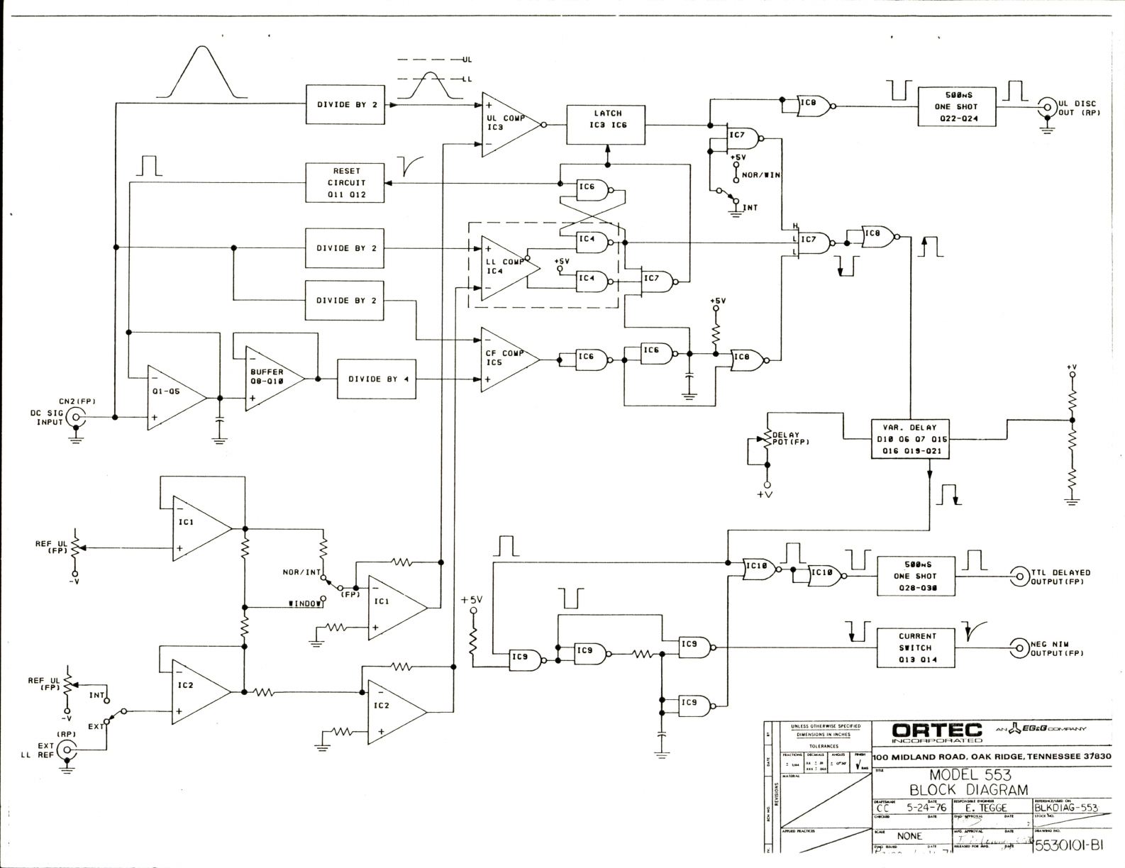
S00NS
ONE
SHOT
□22-02-4
UL
DISC
DIVIDE
BY
2
OUT
(RP)
LATCH
IC3
ICS
UL
COM
IC3
♦sv
NOR/lIN
RESET
CIRCUIT
Oil
012
U
DIVIDE
BY
2
DIVIDE
BY
2
CF
coy
ICS
BUFFER
Oe-QIB
DIVIDE
BY
4
01-05
CN2
FPl
DC
SIC
INPUT
VAR.
DELAY
010
OS
07
015
016
019-021
REF
UL
IFP)
500n8
ONE
SHOT
026-030
IC10
NOR/INT
[C10
[FPJ
■INOOi
CURRENT
SilTCH
013014
REF
UL
3!^
(RP)
LL
REF
TTL
DELAYED
OUTPUTCFP)
®NEC
NIM
OUTPUTtF
ORTEC
A
Ai
tica
100
MIDLAND
ROAD,
OAK
RIDGE,
TENNESSEE
37830
MODEL
553
BLOCK
DIAGRAM
CC
5-24-76
E.
TEGGE
UfHINCr/IMS
ON
BLKDIAG-553
C>KM»
OATI
SAII
NONE
'■
'
•
//.
^
5530101-Bi
.
r:

*C3SD-
—CUE}—
CSE)
-CSIS-
—HQ^ah-
—it^ei—
I
6?l»
>N\SJ.V3H
—i-ytai—
cmi—
k
—CsSS)—
^linlui
Mmsj-wijf,
-iUS}—
—HHD—
0
^^
0
m
ff
i
0
3
B.
-+CSS—
i£±
LM\%'L
.©
(D^.0
©
0
W
5
^
<
V-
A
'A"
Table of contents
Other EG&G Measuring Instrument manuals


