EG&G ORTEC 458 Service manual

A
iNj
^.^EEs.G
cz:
a
r\/i
F='A
rxi
N'
Model
458
Pulse
Shape
Analyzer
.5^

ORTEC
458
PULSE
SHAPE
ANALYZER
Manual
Change
Sheet
March
8,1972
ECN3
In
Fig.
3.1
on
page
3,
negative-going
pulses
are
shown
for
each
of
the
four
indicated
pulses.
This
is
in
error;
all
four
should
be
positive-going
pulses
and
are
inverted
from
the
waveforms
that
will
be
seeen
on
an
oscil
loscope.
On
Schematic
458-0201-S1,
change
the
connection
from
the
collector
of
Q21
to
the
cathode
of
D24
to
show
that
it
is
actually
connected
from
the
col
lector
of
Q21
to
the
anode
of
D24.
On
Schematic
458-0301-SI,
change
the
value
of
R74
from
1.33K
to
1.47K;
change
the
value
of
C12
from
15
pF
to
10
pF;
add
RMS,
422
ohms
1%,
1/8
W,
MFTO
in
series
between
R31
and
the
junction
of
TP3,R78,
R79,
C11,
and
the
collector
of
Q14.
L
j

Model
458
Pulse
Shape
Analyzer
Operating
and
Service
Manual
Printed
in
U.S.A.
©
ORTEC
Incorporated
1971
993
03C
1171
02

STANDARD
WARRANTY
FOR
ORTEC
INSTRUMENTS
ORTEC
warrants
its
instruments
other
than
preampl
ifier
FET
input
transistors,
vacuum
tubes,
fuses,
and
batteries
to
be
free
from
defects
in
workmanship
and
materials
for
a
period
of
twelve
months
from
date
of
shipment
provided
that
the
equipment
has
been
used
in
a
proper
manner
and
not
subjected
to
abuse.
Repairs
or
replace
ment,
at
ORTEC
option,
wil
l
be
made
on
in-warranty
instruments,
without
charge,
at
the
ORTEC
factory.
Shipping
expense.wi
l
l
be
to
the
account
of
the
customer
except
in
cases
of
defects
discovered
upon
initial
operation.
Warranties
of
vacuum
tubes
and
semiconductors
made
by
their
manufacturers
wil
l
be
extended
to
our
customers
only
to
the
extent
of
the
manufacturers'
l
iabi
l
ity
to
ORTEC.
Special
ly
selected
vacuum
tubes
or
semiconductors
cannot
be
warranted.
ORTEC
reserves
the
right
to
modify
the
design
of
its
products
without
incurring
responsibil
ity
for
modification
of
previously
manufactured
units.
Since
in
stal
lation
conditions
are
beyond
our
control,
ORTEC
does
not
assume
any
risks
or
l
iabil
ities
associated
with
methods
of
instal
lation
or
with
instal
lation
results.
QUALITY
CONTROL
Before
being
approved
for
shipment,
each
ORTEC
in
strument
must
pass
a
stringent
set
of
qual
ity
control
tests
designed
to
expose
any
flaws
in
materials
or
workmanship.
Permanent
records
of
these
tests
are
maintained
for
use
in
warranty
repair
and
as
a
source
of
statistical
information
for
design
improvements.
ORTEC
must
be
informed
in
writing
of
the
nature
of
the
fault
of
the
instrument
being
returned
and
of
the
model
and
serial
numbers.
Fai
lure
to
do
so
may
cause
unnecessary
delays
in
getting
the
unit
repaired.
Our
standard
procedure
requires
that
instruments
returned
for
repair
pass
the
same
quality
control
tests
that
are
used
for
new-production
instruments.
Instruments
that
are
returned
should
be
packed
so
that
they
wil
l
withstand
normal
transit
handling
and
must
be
shipped
PREPAID
via
Air
Parcel
Post
or
United
Parcel
Service
to
the
nearest
ORTEC
repair
center.
Instru
ments
damaged
in
transit
due
to
inadequate
packing
wi
ll
be
repaired
at
the
sender's
expense,
and
it
wil
l
be
the
sender's
responsibi
lity
to
make
claim
with
the
shipper.
Instruments
not
in
warranty
will
be
repaired
at
the
standard
charge
unless
they
have
been
grossly
misused
or
mishandled,
in
which
case
the
user
wi
ll
be
notified
prior
to
the
repair
being
done.
A
quotation
wil
l
be
sent
with
the
notification.
DAMAGE
IN
TRANSIT
Shipments
should
be
examined
immediately
upon
receipt
for
evidence
of
external
or
concealed
damage.
The
carrier
making
del
ivery
should
be
notified
immediately
of
any
such
damage,
since
the
carrier
is
normal
ly
liable
for
damage
in
shipment.
Packing
materials,
waybi
l
ls,
and
other
such
documentation
should
be
preserved
in
order
to
establ
ish
claims.
After
such
notification
to
the
carrier,
please
notify
ORTEC
of
the
circumstances
so
that
we
may
assist
in
dam
age
claims
and
in
providing
replacement
equipment
if
necessary.

Ill
CONTENTS
Page
WARRANTY
ii
PHOTOGRAPHS
iv
1.
GENERAL
DESCRIPTION
1
2.
SPECIFICATIONS
2
3.
INSTALLATION
3
3.1
General
3.2
Connection
to
Power
3.3
Connection
to
Linear
Amplifier
Output
3
3
3
4.
OPERATION
4
4.1
General
4.2
Front
Panel
Controls
4
4
5.
CIRCUIT
DESCRIPTION
5
5.1
General
5.2
Detailed
Circuit
Description
5
5
6.
MAINTENANCE
9
6.1
Testing
Performance
6.2
Calibration
Adjustments
6.3
Walk
Adjustment
6.4
Troubleshooting
9
9
9
10
7.
APPLICATIONS
11
7.1
Neutron-Gamma
Discrimination
with
Stilbene
and
Liquid
Scintillators
7.2
Neutron—Gamma-Ray
Discrimination
in
Proportional
Counters
7.3
Rise-Time
Discrimination
in
X-Ray
Proportional
Counter
11
13
14
REFERENCES
15
BLOCK
DIAGRAM
and
SCHEMATICS
458-0101-B1
458-0201-SI
458-0301-SI
LIST
OF
FIGURES
Fig.
3.1.
Waveforms
Observed
at
Test
Point
TP1
Fig.
5.1.
458
Timing
Diagram
Fig.
7.1.
Calculated
Response
for
(a)
100
keV
and
(b)
70
keV
Electron
Equivalent
3
6
Energies
Deposited
in
NE-213
12
Fig.
7.2.
Single
Delay
Line
Shaped
Signal
12
Fig.
7.3.
Block
Diagram
for
a
Typical
Neutron-Gamma
Separation
Experiment
13
Fig.
7.4.
Neutron-Gamma
Rise
Time
Spectrum
13
Fig.
7.5.
A
Typical
Neutron
and
Gamma
Rise
Time
Spectrum
from
a
Proton
Recoil
Proportional
Counter
13
Fig.
7.6.
Neutron-Gamma
Discrimination
System
with
Proportional
Counter
13
Fig.
7.7.
Background
Reduction
System
for
an
X-Ray
Proportional
Counter
14
Fig.
7.8.
Suggested
System
for
Setting
the
PSA
Window
of
the
458
14
Fig.
7.9.
Pulse
Shape
Spectrum
Taken
with
Proportional
Counter
System
Shown
in
Fig.
7.8
14

ORTEC^
^
MODEL
458
PULSE
SHAPE
ANALYZER
TIME
RANGE
0,6
0
4
,
0.8
INPUT
DISC.
»Sec
Volts
WALK
UPPER
LEVEL
LOWER
LEVEL
PSA
TIME
WINDOW
INPUT
WINDOW
'
L
Q
N
E
A
G
UL
c
OUTPUT
i
OUTPUT
1
SEIL
iriiniT
Dific.
e.
OliTiniT
y«€/
mZQ
'•fSf*
1
t
-.i-
■#
,L.-

ORTEC
458
PULSE
SHAPE
ANALYZER
1.
GENERAL
DESCRIPTION
The
ORTEC
458
Pulse
Shape
Analyzer
measures
the
fal
l
time
of
an
input
pulse
from
a
shaping
ampl
ifier
and
generates
a
l
inear
output
pulse
with
an
amplitude
that
is
proportional
to
the
fal
l
time.
It
also
includes
a
single
channel
analyzer
that
can
generate
either
of
two
logic
output
pulses,
based
on
the
measured
fal
l
time.
One
of
the
single
channel
logic
outputs
occurs
when
the
time
is
within
the
single-channel
window;
the
other
occurs
when
the
upper
level
setting
is
exceeded.
A
separate
logic
output
occurs
when
the
input
pulse
ampl
itude
exceeds
the
input
discriminator
threshold.
The
ORTEC
458
accepts
input
pulses
from
any
shaping
ampl
ifier,
RC,
active-filter,
or
delay-l
ine.
Its
l
inear
output
is
interpreted
as
a
measurement
of
the
pulse
shape
of
the
input
signal
.
The
output
is
independent
of
the
ampl
itude
of
the
input
and
depends
only
on
the
shape
(waveform)
of
the
input
signal
as
a
function
of
time.
The
shape
of
the
main
shaping
amplifier
output
varies,
depending
on
certain
experimental
conditions.
Although
there
are
several
examples
of
such
variations,
perhaps
the
best
known
is
the
neutron
and
gamma
response
in
certain
scinti
l
lators.
The
conditions
on
the
electronics
in
this
case
are
stringent
because
of
the
nonl
inear
response
of
the
scinti
l
lator
as
a
function
of
neutron
energy.
For
neutrons
with
energies
from
200
keV
to
10
MeV,
the
response
of
an
NE-213
scintil
lator
can
vary
over
a
500:1
range.
The
458
can
operate
satisfactorily
over
a
400:1
dynamic
range
in
these
neutron-gamma
appl
ications,
and
this
has
not
been
possible
heretofore.
This
unit
is
also
appl
icable
for
use
with
gaseous
detectors
for
particle
identification.
Gaseous
detectors
are
designed
so
that
the
charge
col
lection
time
(and
therefore
the
resulting
pulse
shape)
is
influenced
by
the
location
of
the
interaction
within
the
detector,
and
the
interaction
site
is
related
to
the
interacting
particle
type.
Another
appl
ication
of
pulse-shape
analysis
is
with
large
Ge(Li)
semiconductor
detectors.
With
the
458
events
that
interact
within
the
desired
portion
of
the
detector
can
be
selected,
and
those
that
occur
in
low
electric-field-strength
regions
can
be
rejected,
thereby
optimizing
the
energy
resolution
of
the
system.
Some
typical
appl
ications
of
the
458
for
timing
ex
periments
are
described
in
Section
7.
The
input
signal
from
the
main
amplifier
covers
the
0-
to
10-V
range.
The
input
discriminator
covers
the
complete,
range
from
20
mV
to
10
V.
The
input
wi
l
l
be
approxi
mately
symmetrical
for
delay-l
ine
and
active-fi
lter
amp
l
ifier
inputs.
For
classical
RC
fi
ltering
the
fal
l
time
wi
l
l
be
substantial
ly
longer
than
the
rise
time.
For
al
l
inputs
the
time
range
switch
should
be
set
to
be
equal
to
or
greater
than
the
fal
l
time
of
the
input.
Time
ranges
from
0.2
to
10
ftsec
are
selectable.
A
pulse-shape
analysis
"time
window"
is
provided
for
selection
of
a
time
region
within
the
time
range.
With
this
window
a
logic
gating
pulse
can
be
provided
for
al
l
input
pulses
that
have
a
preselected
shape
within
this
time
region.
In
this
way,
for
example,
al
l
neutron
events
can
generate
a
control
function
through
the
window
output,
whereas
the
gamma-ray
events
wi
l
l
produce
no
control
outputs.
2.
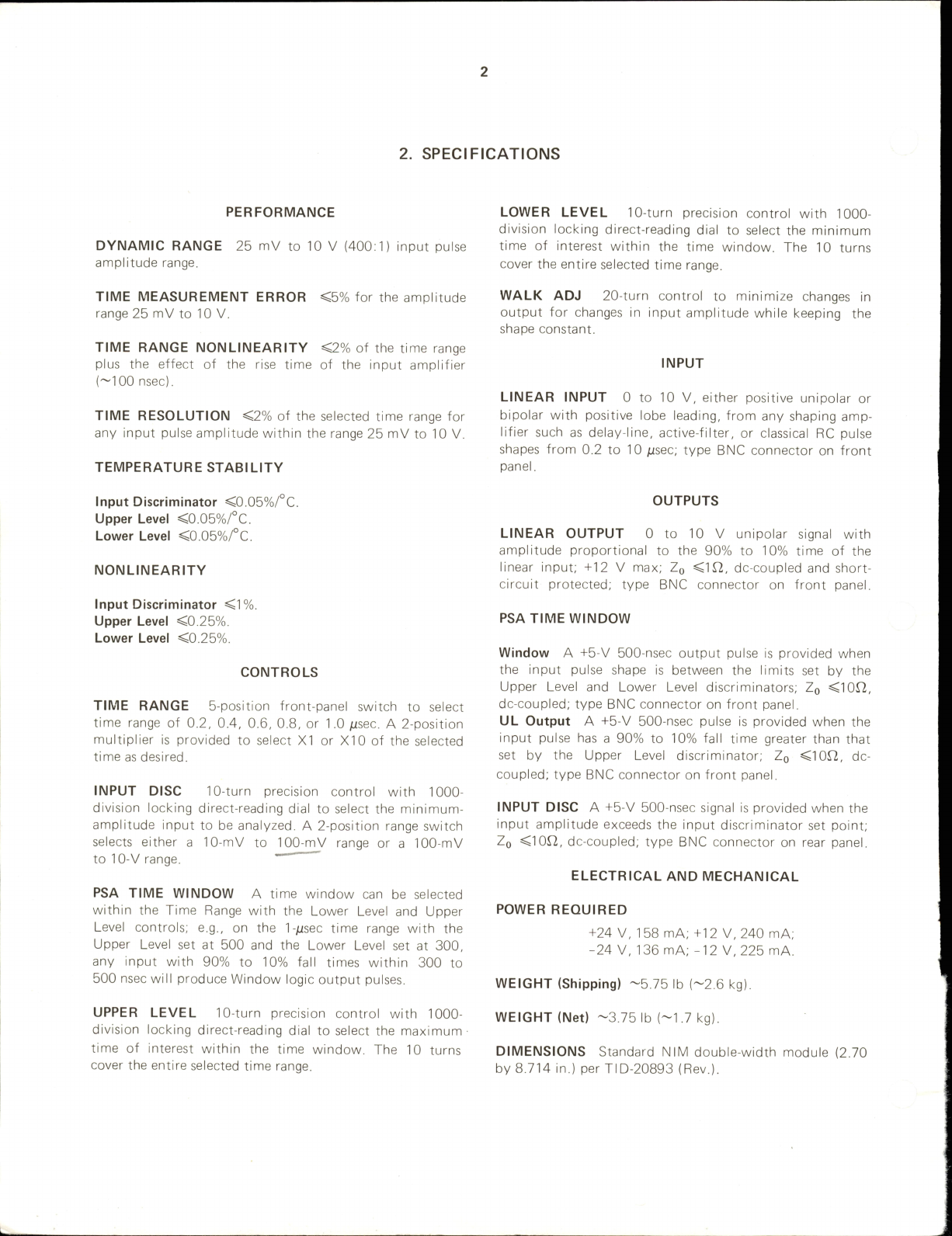
SPECIFICATIONS
PERFORMANCE
DYNAMIC
RANGE
25
mV
to
10
V
(400:1)
input
pulse
ampl
itude
range.
TIME
MEASUREMENT
ERROR
<5%
for
the
ampl
itude
range
25
mV
to
10
V.
TIME
RANGE
NONLINEARITV
<2%
of
the
time
range
plus
the
effect
of
the
rise
time
of
the
input
amplifier
(~100
nsec).
TIME
RESOLUTION
<2%
of
the
selected
time
range
for
any
input
pulse
ampl
itude
within
the
range
25
mV
to
10
V.
TEMPERATURE
STABILITY
LOWER
LEVEL
10-turn
precision
control
with
1000-
division
locking
direct-reading
dial
to
select
the
minimum
time
of
interest
within
the
time
window.
The
10
turns
cover
the
entire
selected
time
range.
WALK
ADJ
20-turn
control
to
minimize
changes
in
output
for
changes
in
input
amplitude
while
keeping
the
shape
constant.
INPUT
LINEAR
INPUT
0
to
10
V,
either
positive
unipolar
or
bipolar
with
positive
lobe
leading,
from
any
shaping
amp
l
ifier
such
as
delay-l
ine,
active-fi
lter,
or
classical
RC
pulse
shapes
from
0.2
to
10
/tsec;
type
BNC
connector
on
front
panel
.
Input
Discriminator
<0.05%/°C.
Upper
Level
<0.05%/°C.
Lower
Level
<0.05%/°C.
NONLINEARITY
Input
Discriminator
<1%.
Upper
Level
<0.25%.
Lower
Level
<0.25%.
CONTROLS
TIME
RANGE
5-position
front-panel
switch
to
select
time
range
of
0.2,
0.4, 0.6, 0.8,
or
1.0
fisec.
A
2-position
multipl
ier
is
provided
to
select
XI
or
XI0
of
the
selected
time
as
desired.
INPUT
DISC
10-turn
precision
control
with
1000-
division
locking
direct-reading
dial
to
select
the
minimum-
ampl
itude
input
to
be
analyzed.
A
2-position
range
switch
selects
either
a
10-mV
to
100-mV
range
or
a
100-mV
to
10-V
range.
'
'
PSA
TIME
WINDOW
A
time
window
can
be
selected
within
the
Time
Range
with
the
Lower
Level
and
Upper
Level
controls:
e.g.
,
on
the
1-/tsec
time
range
with
the
Upper
Level
set
at
500
and
the
Lower
Level
set
at
300,
any
input
with
90%
to
10%
fal
l
times
within
300
to
500
nsec
wi
l l
produce
Window
logic
output
pulses.
UPPER
LEVEL
10-turn
precision
control
with
1000-
division
locking
direct-reading
dial
to
select
the
maximum-
time
of
interest
within
the
time
window.
The
10
turns
cover
the
entire
selected
time
range.
OUTPUTS
LINEAR
OUTPUT
0
to
10
V
unipolar
signal
with
ampl
itude
proportional
to
the
90%
to
10%
time
of
the
linear
input;
+12
V
max;
Zq
<1^2,
dc-coupled
and
short-
circuit
protected;
type
BNC
connector
on
front
panel
.
PSA
TIME
WINDOW
Window
A
+5-V
500-nsec
output
pulse
is
provided
when
the
input
pulse
shape
is
between
the
l
imits
set
by
the
Upper
Level
and
Lower
Level
discriminators;
Zq
<1012,
dc-coupled;
type
BNC
connector
on
front
panel
.
UL
Output
A
+5-V
500-nsec
pulse
is
provided
when
the
input
pulse
has
a
90%
to
10%
fal
l
time
greater
than
that
set
by
the
Upper
Level
discriminator;
Zq
<10^2,
dc-
coupled;
type
BNC
connector
on
front
panel
.
INPUT
DISC
A
+5-V
500-nsec
signal
is
provided
when
the
input
ampl
itude
exceeds
the
input
discriminator
set
point;
Zq
<10L2,
dc-coupled;
type
BNC
connector
on
rear
panel
.
ELECTRICAL
AND
MECHANICAL
POWER
REQUIRED
+24
V,
158
mA;
+12
V,
240
mA;
-24
V,
136
mA;
-12
V,
225
mA.
WEIGHT
(Shipping)
~5.75
lb
(~2.6
kg).
WEIGHT
(Net)
-3.75
lb
(-1.7
kg).
DIMENSIONS
Standard
NIM
double-width
module
(2.70
by
8.714
in.)
per
TID-20893
(Rev.).

3.
INSTALLATION
3.1.
GENERAL
The
ORTEC
458
contains
no
internal
power
but
must
be
used
in
conjunction
with
an
ORTEC
401/402
Series
Bin
and
Power
Supply,
which
is
intended
for
rack
mounting.
Therefore
if
other
equipment
is
operated
in
the
same
rack
(particularly
vacuum
tube
equipment)
there
must
be
sufficient
cool
ing
air
circulating
to
prevent
any
local
ized
heating
of
the
al
l-transistorized
circuitry
of
the
458.
The
temperature
of
equipment
mounted
in
racks
can
easi
ly
exceed
the
recommended
maximum
unless
these
pre
cautions
are
taken.
The
458
should
not
be
subjected
to
temperatures
in
excess
of
120°F
(50°C).
To
obtain
maximum
temperature
insensitivity,
the
458
should
not
be
exposed
to
high
velocity
drafts
of
cool
ing
air,
especial
ly
if
the
temperature
of
the
cool
ing
air
is
not
stable.
3.2.
CONNECTION
TO
POWER
The
Power
Supply
to
the
401
Bin
should
be
turned
off
when
modules
are
inserted
or
removed.
ORTEC
modular
instruments
are
designed
so
that
it
is
not
possible
to
overload
the
Power
Supply
with
a
ful
l
complement
of
modules
in
the
Bin.
Since,
however,
this
may
not
be
true
if
the
Bin
contains
modules
other
than
those
of
ORTEC
design,
the
Power
Supply
voltages
should
be
checked
after
the
modules
are
inserted.
The
ORTEC
401
Series
Bin
has
test
points
on
its
Power
Supply
control
panel
to
monitor
the
dc
voltages.
The
Power
Supply
voltages
should
read
within
±0.5%
of
the
nominal
values
for
proper
operation
of
NIM-standard
instruments.
3.3.
CONNECTION
TO
LINEAR
AMPLIFIER
OUTPUT
(a)
Pulse
Shape.
(b)
Baseline
Offset
with
R46
Adjusted
Too
Far
Clockwise.
/
u-y
The
input
to
the
458
is
furnished
through
a
front
panel
BNC
connector.
The
input
circuit
can
accept
0-
to
10-V
unipolar
signals
into
a
1000T2
load.
The
input
operating
range
is
from
100
mV
to
10
V
when
the
Input
Disc
range
switch
is
set
at
10
V.
When
the
switch
is
set
at
0.1.V,
the
input
operating
range
is
from
20
mV
to
10
V,
but
precautions
must
be
observed
to
obtain
this
wider
dynamic
range.
Use
the
fol
lowing
procedure
with
the
switch
set
at
0.1
V:
1.
If
the
l
inear
amplifier
has
a
dc
output
adjustment,
adjust
the
output
level
careful
ly
to
0
+
5
mV.
The
rise
time
of
the
output
pulse
should
be
less
than
1
/tsec.
2.
Use
a
pulse
generator
to
furnish
pulses
through
the
ampl
ifier.
Adjust
the
pulse
generator
ampl
itude
and
the
ampl
ifier
gain
for
an
amplifier
output
of
2
V.
Connect
this
to
the
458
Input.
3.
Connect
an
oscil
loscope
probe
to
test
point
TP1,
accessible
through
the
top
of
the
458.
Set
the
osci
l
loscope
for
0.5
V/division
and
1
^tsec/division.
The
osci
l
loscope
trace
should
be
similar
to
that
shown
in
Fig.
3.1a.
4.
Set
the
osci
lloscope
sensitivity
to
50
mV/division
and
adjust
R46,
located
between
the
test
point
and
the
front
(c)
Baseline
Offset
with
R46
Adjusted
Correctly.
(d)
Baseline
Offset
with
R46
Adjusted
Too
Far
Counterclockwise.
Fig.
3.1.
Waveforms
Observed
at
Test
Point
TP1.
panel,
for
a
zero
basel
ine
offset
simi
lar
to
that
in
Fig.
3.1c.
If
R46
does
not
have
sufficient
range
to
obtain
the
zero
basel
ine
offset,
use
R4
as
a
coarse
adjustment
and
then
complete
the
adjustment
of
R46.
5.
The
Input
Disc
dial
has
1000
divisions,
corresponding
to
its
range
of
100
mV.
Set
the
control
as
desired,
between
100
and
1000
dial
divisions,
to
determine
the
minimum
input
pulse
amplitude
that
wi
l
l
trigger
a
time
measurement.

4.
OPERATION
4.1.
GENERAL
The
ORTEC
458
Pulse
Shape
Analyzer
measures
the
time
during
which
the
input
waveform
falls
from
90%
of
its
peak
amplitude
to
10%
of
its
peak
amplitude,
pro
viding
the
peak
amplitude
is
sufficient
to
trigger
the
458
input
discriminator.
When
the
shape
of
the
input
pulse
varies,
due
to
the
nature
of
the
information
furnished
into
the
l
inear
ampl
ifier
preceding
the
458,
the
fal
l
time
of
the
pulse
wi
l l
vary
and
wi
l l
provide
a
variation
of
the
l
inear
output
ampl
itude
that
is
proportional
to
the
measured
time.
After
the
decay
time
has
been
converted
into
a
linear
output
pulse,
with
an
ampl
itude
range
of
0
to
10
V
corresponding
to
the
selected
time
range,
the
variety
of
pulse
ampl
itudes
that
are
avai
lable
through
the
l
inear
output
wil
l
reflect
the
nature
of
the
experiment.
For
example,
there
wi
l
l
be
two
principal
concentrations
of
pulse
heights
for
the
gamma-neutron
appl
ication,
whereas
an
experiment
that
identifies
the
location
of
interaction
in
a
detector
could
provide
a
fairly
equal
distribution
of
ampl
itudes
throughout
the
range,
iftus
the
adjustment
of
the
controls
for
the
single
channel
analyzer
and
the
uses
for
its
logical
outputs
wil
l
depend
upon
the
nature
of
the
experiment.
See
the
appl
ications
in
Section
7
for
further
suggestions.
4.2.
FRONT
PANEL
CONTROLS
TIME
RANGE
The
total
range
for
the
time
measurement
can
be
as
short
as
200
nsec
or
as
long
as
10
/jsec.
The
selected
range
wi
l l
be
converted
to
a
0-
to
10-V
range
of
l
inear
outputs.
The
appropriate
range
wi
ll
be
one
that
is
long
enough
to
accommodate
the
slowest
fal
l
time
but
is
as
short
as
possible
within
this
restriction.
INPUT
DISC
The
input
discriminator
must
be
triggered
by
an
input
pulse
in
order
for
its
fall
time
to
be
measured.
The
ampl
itude
of
the
input
pulse
from
the
l
inear
amplifier
is
the
parameter
that
is
measured
by
this
function.
When
the
sl
ide
switch
is
set
at
1
V,
the
10-turn
potentiometer
can
be
set
for
any
level
between
10
and
1000
dial
divisions,
corresponding
to
an
input
ampl
itude
range
of
100
mV
through
10
V.
For
a
more
precise
setting
at
lower
levels
the
sl
ide
switch
can
be
set
at
0.1
V,
and
the
usable
range
for
the
10-turn
potentiometer
is
then
about
100
dial
divisions
through
1000
divisions,
or
about
10
mV
through
100
mV.
When
the
input
discriminator
is
trig
gered,
there
is
a
logic
output
pulse
through
the
rear
panel
BNC
designated
Input
Disc
Output.
WALK
ADJ
The
purpose
of
this
screwdriver
control
is
to
minimize
the
walk
when
measuring
decay
times
for
differing
input
pulse
ampl
itudes.
See
Section
6
for
cali
bration
information.
PSA
TIME
WINDOW
These
two
10-turn
potentiometers
are
the
controls
that
set
the
two
discriminator
levels
of
the
single
channel
analyzer
that
analyzes
the
l
inear
output
signal
of
the
458.
Since
any
selected
time
range
wil
l
be
converted
into
a
0-
to
10-V
linear
output
range,
the
1000
dial
divisions
on
each
potentiometer
are
directly
related
to
the
selected
time
range.
Whatever
their
settings
for
any
specific
appl
ication,
a
linear
output
amplitude
that
exceeds
the
Upper
Level
setting
wi
l
l
generate
a
logic
output
through
the
UL
connector
and
wil
l
inhibit
a
Window
output.
A
linear
output
ampl
itude
that
exceeds
the
Lower
Level
setting
but
does
not
also
exceed
the
Upper
Level
setting
wi
l l
generate
a
Window
output.
5.
CIRCUIT
DESCRIPTION
5.1.
GENERAL
A
block
diagram,458-0101-B1,
is
included
at
the
back
of
this
manual
.
There
are
also
three
schematics,
458-0201-SI
(Sheets
1
and
2)
and
458-0301-SI.
The
fol
lowing
circuit
description
refers
primarily
to
the
block
diagram.
The
ORTEC
458
Pulse
Shape
Analyzer
consists
of
three
basic
functions:
Input
and
Compression
Circuitry,
Dual
Constant-Fraction
Discriminator,
and
a
Time
to
Pulse
Height
Converter.
These
three
basic
functions
lead
to
the
generation
of
a
l
inear
output.
A
single
channel
analyzer
is
also
included
for
logical
analysis
of
the
l
inear
output
ampl
itudes.
The
input
and
compression
circuitry
provides
isolation
and
transforms
the
input
pulse
height
range
of
20
mV
to
10
V
into
a
range
of
100
mV
to
5
V.
The
effective
compression
is
from
500:1
down
to
only
50:1
in
pulse
height
variation.
The
Dual
Constant-Fraction
Discriminator
generates
two
time
markers.
The
first
time
marker
is
generated
at
a
point
on
the
trai
l
ing
edge
of
the
unipolar
input
pulse
when
the
pulse
has
decayed
to
approximately
90%
of
its
peak
ampl
itude.
The
second
marker
is
generated
when
the
input
pulse
has
decayed
to
approximately
10%
of
its
peak
ampl
itude.
The
Time
to
Pulse
Height
Converter
then
measures
the
time
between
the
90%
and
10%
markers
and
stores
the
time
information
on
a
capacitor.
The
voltage
on
the
capacitor
is
strobed,
shaped,
and
routed
to
the
l
inear
output.
This
voltage
is
in
the
range
of
0'to
10
V,
independent
of
the
input
ampl
itude
from
the
linear
amplifier.
The
Single
Channel
Analyzer
views
the
l
inear
output
signal
ampl
itude
and
generates
a
Window
output
at
strobe
time
if
the
output
amplitude
is
between
the
settings
of
the
Lower
Level
and
Upper
Level
controls
(UL
set
higher
than
LL).
If
the
ampl
itude
is
greater
than
the
setting
of
the
UL,
a
UL
logic
output
is
generated
at
strobe
time
and
a
Window
output
is
inhibited.
5.2.
DETAILED
CIRCUIT
DESCRIPTION
The
input
signal
is
attenuated
by
a
factor
of
2
by
R1
and
R2,
and
is
routed
to
the
input
unity-gain
ampl
ifier,
Q1
to
Q6
and
Q45.
Diodes
D1
and
D2
prevent
the
absolute
ampl
itude
of
the
signal
from
exceeding
10
V.
The
signal
at
the
emitter
of
Q45
is
routed
to
a
1-jusec
delay
l
ine
and
to
a
voltage
comparator,
IC1
.
The
purpose
of
the
com
parator
is
to
generate
a
logic
signal
when
the
input
signal
exceeds
+^
V.
When
the
Input
Disc
range
is
set
for
0.1
V,
the
logic
signal
starts
a
one-shot
multivibrator,
IC2A,
B,
and
C,
to
control
the
gain
in
the
compression
network.
For
this
condition
the
initial
gain
of
the
network
is
10
and
it
is
shifted
to
unity
when
the
input
logic
starts
the
one-shot.
The
signal
compressor
is
essentially
a
l
inear
gate
that
routes
the
signal
through
an
inverting
operational
amp
l
ifier
with
a
gain
of
10
if
the
input
signal
does
not
exceed
-1-1
V,
or
through
another
operational
amplifier
with
unity
gain
if
the
input
signal
does
exceed
-i-l
V.
The
decision
on
whether
or
not
the
input
signal
exceeds
the
-i-1-V
level
is
made
as
previously
described
by
IC1.
The
input
signal
is
delayed
1
fisec
by
DLi
and
inverted
by
operational
amp
l
ifier
0A1.
Thus
the
signal
arrives
at
the
compressor
input
after
the
decision
has
been
made
on
what
the
gain
should
be
(see
the
Timing
Diagram,
Fig.
5.1).
The
compressor
gain
is
changed
for
only
the
0.1-V
position
of
the
Input
Disc
switch.
When
the
switch
is
set
at
10
V,
IC2
Is
disabled
and
the
compressor
gain
is
fixed
at
unity.
Assume
that
the
Input
Disc
switch
is
set
at
0.1
V
and
that
the
input
signal
is
less
than
-i-1
V.
IC2C
wil
l
remain
in
its
low
state
of
approximately
zero
volts.
The
current
through
R33
is
routed
equally
through
R32
and
R34.
The
collector
of
Q9
is
at
approximately
-4
V.
The
base
of
transistor
IC3B
is
biased
at
~-3.3
V.
Thus
transistor
IC3A
is
turned
off
and
IC3B
is
turned
on.
Q10
provides
a
constant
current
through
IC3B
that
divides
approximately
equally
through
IC3E
and
IC3F.
For
these
bias
conditions
IC3E
and
IC3F
form
the
differential
input
to
a
high-gain
operational
ampl
ifier
that
includes
Q11
to
Q15.
The
negative
voltage
signal
from
pin
10
of
0A1
is
converted
to
a
current
signal
through
R27
and
generates
a
voltage
signal
across
R28
of
approximately
(R28/R27)Vio,
or
(10K/-
1
KjVio
=
lOVio.
In
other
words,
the
signal
at
pin
10
of
0A1
is
ampl
ified
by
a
factor
of
10
through
the
compressor.
If
a
signal
of
ampl
itude
greater
than
-i-1
V
is
presented
at
the
input,
the
output
of
the
one-shot
multivibrator
IC2C
is
switched
from
its
low
state
to
its
high
state
{~+2
V).
IC3A
is
turned
on
and
IC3B
is
turned
off.
The
input
signal
then
passes
through
R29
and
R30
to
the
compressor
output
with
a
gain
of
unity.
The
one-shot
IC2C
output
at
pin
8
remains
in
the
high
state
for
approximately
8
/tsec
or
until
the
input
signal
has
completely
disappeared.
This
is
dead
time
and
exists
only
for
those
input
pulses
with
ampl
itudes
between
1
and
10
V
when
the
Input
Disc
switch
is
set
at
0.1
V.
The
output
of
the
compressor
circuit
is
ac-coupled
through
C20
and
routed
to
basel
ine
restorer
Q36
to
Q39,
shown
on
schematic
458-0201-SI,
Sheet
2.
This
is
an
active
type
of
dc
restorer
where
the
signal
basel
ine
at
the
base
of
Q37
is
compared
with
the
voltage
at
the
base
of
Q38.
If
the
signal
basel
ine
is
positive
with
respect
to
ground,
Q37
is
turned
on
and
the
current
through
Q36
is
reduced
to
zero.
For
this
condition
Q39
pul
ls
the
basel
ine
back
toward

7"
90%
7
10%
7
Reset
1
TiSec
Signal
Compressor
Input
Signal
Compressor
(X1
Pos
of
Input
Disc
Only)
Baseline
Restorer
Ouptut
Stretcher
Ouptut
Pulse
Stretcher
&
Linear
Gate
Input
ICG
Timing
Comp
IC7
Timing
Comp
Input
Disc.
Output
I
7
90%
7
10%
7
Reset
TPHC
Start
TPHC
Stop
Start
Tunnel
Diode
Memory
Stop
Inhibit
Gate
Stop
Tunnel
Diode
Memory
Conversion
Cap
Voltage
Gate
Width
Generator
Linear
Output
TPHC
Reset
Window
Output
-
0.5
iusec
'1
Msec
1
Msec
b
I
1
UL
Output
(only
if
UL
Disc,
exceeded)
J
L
Fig.
5.1.
458
Timing
Diagram.

zero
volts.
If
the
basel
ine
goes
negative,
Q37
turns
off
and
approximately
3
mA
of
current
flows
through
Q36
to
bring
the
basel
ine
back
toward
zero
very
rapidly.
After
the
baseline
is
restored,
the
signal
is
routed
into
three
level
discriminators,
IC5, IC6,
and
IC7,
and
to
a
pulse
stretcher,
Q16
through
Q29.
When
the
signal
goes
positive,
stretcher
capacitor
C28
is
charged
by
the
current
through
Q25.
The
voltage
on
C28
is
control
led
by
the
closed-loop
unity-gain
amplifier,
Q23
to
Q28,
which
feeds
the
C28
voltage
back
to
the
gate
of
the
input
differential
pair.
If
the
voltage
on
C28
tries
to
exceed
that
of
the
input
signal,
Q17
turns
on
and
Q16
turns
off
to
reverse-bias
Q19
and
Q20.
With
Q19
and
Q20
turned
off,
the
voltage
on
C28
ceases
to
increase.
All
this
is
the
action
of
the
stretcher
before
the
input
reaches
its
peak.
When
the
input
signal
reaches
its
peak
and
starts
to
decrease,
diode
D24
reverse-
biases.
The
charge
on
C28,
which
is
equal
to
the
peak
amplitude
of
the
input
pulse,
wil
l
remain,
providing
that
the
gate
transistor,
Q22,
is
turned
off
before
the
peak
has
been
reached.
The
voltage
on
C28
is
routed
to
the
output
of
the
stretcher
and
to
the
base
of
Q32
through
the
unity-gain
ampl
ifier,
Q23
to
Q28.
The
gate
signal
for
the
stretcher
is
derived
from
the
level
discriminator,
IC5.
The
positive
signal
comes
from
the
baseline
restorer,
Q36
to
Q39,
to
the
IC5
discriminator.
The
ampl
itude
of
the
signal
that
is
required
to
change
the
IC5
discriminator
state
from
low
to
high
is
determined
by
the
Input
Disc
10-turn
front
panel
control
and
by
the
range
that
is
set
by
its
slide
switch
(a
function
not
shown
on
the
block
diagram).
The
Input
Disc
control
sets
a
positive
voltage
on
pin
2
of
IC5.
When
the
signal
exceeds
the
pin-2
voltage,
IC5
changes
states
from
high
to
low
and
generates
a
negative
output
pulse.
This
negative
pulse
is
inverted
through
IC4A
to
trigger
a
one-shot
multivibrator,
IC4B
and
IC4C.
The
multivibrator
output
is
routed
through
IC4D
and
transistor
Q29
to
the
base
of
Q22,
the
stretcher
gate
transistor.
The
gate
signal
reaching
the
base
of
Q22
is
negative
enough
to
turn
Q22
off.
The
output
of
IC4C
remains
in
the
positive
state
until
the
system
reset
is
generated
(see
Fig.
5.1).
The
one-shot
multivibrator,
IC4B
and
IC4C,
also
triggers
a
second
0.5-/tsec
one-shot
multivibrator,
IC2D,
Q7,
and
Q8.
The
output
at
QBE-
is
routed
to
the
rear
panel
BNC
connector.
Input
Disc
output.
The
stretcher
output
is
routed
to
a
l
inear
gate,
Q32
to
Q35,
which
is
normally
closed.
The
same
signal
that
opened
the
stretcher
is
routed
to
the
base
of
Q34,
which
is
normal
ly
on.
When
Q34
is
turned
on,
its
current
holds
the
base-emitter
junction
of
Q32
reverse-biased,
and
this
prevents
the
stretcher
signal
from
reaching
pin
2
of
IC6
and
IC7.
Before
Q34
is
turned
off
by
the
gate
signal,
a
negative
voltage
is
forced
on
the
base,
of
Q33
which
is
transferred
to
pin
2
of
IC6
and
IC7.
This
causes
discriminators
ICG
and
IC7
toassumea
low
voltage
state
before
gate
Q34
is
opened.
When
the
gate
signal
turns
Q34
off,
the
stretcher
signal
is
routed
through
Q32
and
Q34
to
pin
2
of
ICG
and
IC7.
The
stretcher
signal
at
the
emitter
of
Q33
has
an
ampl
itude
with
reference
to
ground
that
is
approximately
90%
of
the
peak
ampl
itude
of
the
signal
presented
at
pin
3
of
ICG
and
IC7.
The
stretcher
signal
is
presented
to
ICG
without
attenuation,
but
this
signal
is
attenuated
further
so
that
the
stretched
signal
at
pin
2
of
IC7
is
approximately
10%
of
the
peak
ampl
itude
of
the
signal
present
at
pin
3.
The
outputs
of
both
discriminators
remain
in
the
low
state
until
a
time
after
the
peak
of
the
input
signal
.
As
the
input
goes
beyond
the
peak
and
decays
toward
zero,
there
is
a
time
when
the
voltage
on
pin
3
of
ICG
is
equal
to
the
90%
stretched
signal
on
pin
2
of
ICG,
and
ICG
changes
from
its
low
state
to
its
high
state
as
the
pin-3
signal
goes
further
negative.
This
generates
the
first
timing
signal
to
start
the
time
measurement
of
the
input
signal
.
The
second
time
marker
is
generated
by
IC7
as
the
signal
voltage
on
pin
3
goes
more
negative
than
the
10%
stretched
signal
on
its
pin
2.
The
output
transition
of
IC7
is
then
from
its
low
state
to
its
high
state,
the
same
as
previously
described
for
ICG.
This
signal
wil
l
stop
the
time
measure
ment
of
the
input
signal
.
The
output
signals
from
both
ICG
and
IC7
are
differ
entiated,
and
the
positive
transitions
are
fed
through
separate
fast
ampl
ifiers
to
the
start
and
stop
inputs
of
the
Time
to
Pulse
Height
Converter.
The
start
time
marker
that
originated
at
ICG
is
routed
through
fast
ampl
ifier
Q1
and
Q2
(see
schematic
458-0301-S1)
to
the
start
input
tunnel
diode
D2
of
the
TPHC.
The
start
signal
triggers
D2
to
its
high
state,
where
it
remains
until
a
system
reset
is
gen
erated.
The
high
state
of
D2
is
routed
through
the
amp
l
ifier
Q3
to
Q6
to
the
conversion
clamp
Q7
to
Q9
and
to
the
stop
inhibit
clamp
Q17.
When
Q17
turns
on,
current
through
R42
is
rerouted
from
tunnel
diode
D10
through
Q17
and
this
sets
the
proper
bias
current
so
that
the
stop
signal
wil
l
be
able
to
change
the
state
of
D10.
The
start
signal
from
D2
turns
Q5
on.
This
forward-biases
Q7
to
turn
off
Q8
and
conversion
clamp
Q9.
The
conversion
current
source
is
normally
on,
providing
current
to
the
clamp
transistor
Q9E.
Before
the
clamp
Q9
is
turned
off,
the
conversion
capacitor
is
clamped
to
near
zero
volts.
When
the
clamp
is
removed,
the
conversion
current
is
rerouted
from
Q9E
to
the
conversion
capacitors
C7
to
C9.
The
voltage
on
the
conversion
capacitor
is
a
ramp
that
increases
in
a
negative
direction.
As
the
conversion
capacitor
is
being
charged,
the
stop
signal
comes
through
the
fast
ampl
ifier
Q15,
Q16
to
cause
D10
to
change
from
a
low
state
to
a
high
negative
state.
This
transition
is
routed
through
ampl
ifier
Q18
and
Q19
to
a
gate-width
generator
and
to
the
conversion
gate
transistor
Q21
.
The
D10
transition
causes
Q21
to
saturate
and
to
take
all
of
the
conversion
current
that
normal
ly
flows
through
Q22.
At
this
time
the
voltage
on
the
conversion
capacitor
ceases
to
increase.
The
capacitor
charge
is
then
proportional
to
the
time
interval
between
the
start
and
stop
signals.
This
stored
signal
is
routed
through
a
unity-gain
FET
amplifier
Q10
to
Q14
and
Q36.
The
output
at
Q36E
is
fed
to
a
fast
operational
amplifier,
OAl.
Operational
ampl
ifier
OAl
serves
two
purposes.
It
inverts
the
converter
signal
and
serves
as
an
output
l
inear
gate.
The
operational
amplifier
has
two
input
signals,
through
R88
and
R89,
and
two
feedback
paths,
R95
and
R96.
In
the
normal
state
before
a
gate
signal
is
generated,
the
current
from
the
-I-24-V
source
flows
through
034
and
R89
to
forward-bias
D14
and
clamp
the
pin-10
output
of
OAl
to
a
negative
voltage
equal
to
approximately
one
diode
junction.
Pin
10
and
the
base
of
Q37
remain
constant
and
inde
pendent
of
the
conversion
voltage
unti
l
a
gate
signal
turns
034
off.
The
gate
signal
originates
from
the
stop
input.
The
stop
input
triggers
a
gate
width
generator
O20
and
Q30
to
032.
The
gate
width
generator
produces
a
gate
signal
at
the
base
of
033
that
is
negative
and
is
about
1
/tsec
wide.
This
negative
signal
turns
033
on
and
034
off.
When
034
turns
off,
the
current
that
normally
forward-biases
D14
is
reduced
to
zero
and
the
conversion
voltage
signal
at
Q36E
causes
a
current
to
flow
through
013
in
the
direction
that
forward-biases
013.
The
current
through
R96
while
034
is
turned
off
is
proportional
to
the
conversion
voltage.
Thus
a
positive
signal,
~1
jjisec
wide,
wi
ll
appear
at
the
base
of
037
and
wi
l
l
be
proportional
to
the
conversion
voltage
during
the
gate
time.
When
034
is
turned
off
and
the
gate
signal
is
not
present,
the
voltage
on
the
base
of
037
wil
l
be
approximately
zero.
The
positive
conversion
signal
is
routed
through
a
buffer
unity-gain
amplifier
037
to
O40
and
presented
to
the
Linear
Output
connector
on
the
front
panel
.
The
conversion
signal
at
the
036E
output
of
the
FET
ampl
ifier
is
fed
to
a
single
channel
analyzer
(SCA).
The
lower
level
discriminator
of
the
SCA
is
IC1
and
the
upper
level
discriminator
is
IC2.
IC1
is
normally
in
the
high
state
and
IC2
is
in
the
low
state.
If
the
lower
level
discriminator
101
is
switched
to
the
low
state
by
the
signal
on
pin
2
and
the
output
of
the
upper
level
discriminator
102
remains
in
the
low
state,
both
Q41
and
Q42
wi
l l
be
turned
off.
If
Q41
and
Q42
are
both
off
at
the
time
that
the
gate
pulse
turns
Q43
off,
a
positive
transition
wil
l
occur
at
the
base
of
Q49
to
trigger
the
one-shot
Q49
to
Q52
and
to
thus
produce
a
standard
positive
logic
output
through
the
Window
con
nector
on
the
front
panel
.
The
logic
condition
that
produces
a
Window
output
requires
that
the
conversion
signal
be
greater
than
the
lower
level
control
setting
and
less
than
the
upper
level
control
setting.
If
the
conversion
signal
ampl
itude
exceeds
the
setting
of
the
upper
level
control,
Q42
is
turned
on
and
this
prevents
a
Window
output
from
being
generated
at
the
gate
signal
time.
102
is
then
in
a
high
state,
and
a
positive
transition
wil
l
occur
when
the
gate
pulse
turns
Q53
off.
This
positive
transition
triggers
the
one-shot
Q45
to
Q48
to
produce
a
standard
logic
pulse
through
the
UL
output
on
the
front
panel
.
A
logic
pulse
through
the
UL
connector
wil
l
be
furnished
for
each
conversion
signal
that
exceeds
the
UL
control
setting,
including
any
conversion
signal
that
exceeds
the
selected
time
range.
When
an
overrange
occurs,
there
wi
l l
be
no
l
inear
output
but
the
UL
logic
signal
wi
ll
be
strobed
and
wi
l l
furnish
an
output.
The
TPHC
is
reset
to
its
initial
state
by
the
trai
ling
edge
of
the
gate
width
generator
Q32
or
by
an
overrange
signal
from
the
conversion
capacitor
through
Q28
and
Q29.
Either
of
these
signals
wi
l
l
trigger
reset
generator
Q24
to
Q27.
When
Q26
of
the
reset
generator
is
turned
off,
D2
resets
to
its
initial
low
state;
this
resets
the
conversion
clamp
Q9E
to
zero
volts,
and
Q17
is
turned
off
to
restore
the
stop
inhibit
clamp
and
reset
D10
to
its
low
state.
D10
resets
the
conversion
gate
Q21
to
the
off
state.
A
reset
signal
from
the
reset
generator
is
also
fed
back
to
the
base
of
Q30
to
reset
the
one-shot
that
follows
the
input
discriminator.
The
reset
of
this
one-shot
closes
the
stretcher
gate
and
the
linear
gate
between
the
stretcher
and
IC6and
IC7.
%

6.
MAINTENANCE
6.1.
TESTING
PERFORMANCE
The
fol
lowing
material
wi
l l
aid
in
instal
l
ing
and
checking
out
the
458.
It
consists
of
information
on
front
panel
controls,
waveforms,
test
points,
and
output
connectors.
Test
Equipment
The
following,
or
equivalent,
test
equip
ment
is
needed:
1.
ORTEC
419
Pulse
Generator
2.
ORTEC
410
Ampl
ifier
3.
Tektronix
547
Oscilloscope
4.
100f2
attenuator
box
Preliminary
Procedures
Before
making
the
functional
checks,
take
the
following
preliminary
steps:
1.
Visually
check
module
for
possible
damage
due
to
shipment.
2.
With
power
off,
plug
module
into
an
ORTEC
401/402
Series
Nuclear-standard
Bin
and
Power
Supply,
and
check
for
proper
mechanical
al
ignment.
3.
Switch
ac
power
on,
and
check
the
dc
power
voltage
at
the
test
points
on
the
402
Power
Supply
control
panel
.
Functional
Checks
The
following
checks
should
be
made
to
assure
the
correct
function
of
the
458:
1.
Connect
the
direct
output
of
the
pulse
generator
to
the
osci
lloscope
trigger.
Connect
the
attenuated
output
of
the
pulse
generator
to
the
input
of
the
ampl
ifier.
Place
all
attenuator
switches
on
the
pulse
generator
to
the
Out
position
except
one
X2
switch.
Adjust
the
pulse
generator
output
and/or
amplifier
gain
control
to
achieve
an
amp
l
ifier
output
pulse
height
of
approximately
10
V,
single
delay
l
ine.
2.
Connect
the
ampl
ifier
output
to
the
458
input.
Set
the
458
Time
Range
at
0.2
/tsec
and
the
multipl
ier
at
XI
.
Set
the
Input
Disc
10-turn
dial
at
100
and
the
multipl
ier
at
10
V.
Set
the
Upper
Level
and
Lower
Level
10-turn
dials
at
100.
Connect
the
linear
output
to
the
osci
l
loscope
and
observe
an
output
approximately
7
V
in
amplitude.
Chang
ing
the
Time
Range
switch
in
0.2-/.isec
increments
from
0.2
to
1
.0
should
decrease
the
output
ampl
itude
by
1/2, 1/3, 1/4,
1/8
(approx.).
Changing
the
multiplier
switch
to
XI0
should
decrease
the
output
ampl
itude
by
a
factor
of
10
(approx.).
3.
Connect
the
Upper
Level
output
to
the
oscil
loscope
and
observe
a
0.5-/isec
pulse
approximately
5.0
V
in
ampl
itude.
Adjust
the
Upper
Level
dial
unti
l
the
UL
output
disap
pears.
Connect
the
Window
output
to
the
osci
lloscope
and
observe
a
0.5-/isec
pulse
approximately
5.0
V
in
ampl
itude.
Adjust
the
Lower
Level
dial
unti
l
the
Window
output
disappears.
The
UL
and
LL
dial
readings
should
be
in
direct
proportion
with
the
Linear
output
amplitude
±20
small
dial
divisions.
For
example,
if
the
Linear
output
has
an
ampl
itude
of
7
V,
the
UL
and
LL
dials
should
read
700
±20
smal
l
dial
divisions.
6.2.
CALIBRATION
ADJUSTMENTS
DC
Adjustments
1.
Adjust
R121
unti
l
the
voltage
at
the
base
of
Q35
(458-0201
board)
is-4.2
V.
This
potentiometer
is
located
near
the
rear
panel
on
the
458-0201
board.
2.
Adjust
R29
until
the
voltage
at
the
gate
of
Q11
(458-0301
board)
is
zero
volts
±10
mV.
This
potentiom
eter
is
located
at
the
bottom
of
the
458-0301
board.
3.
Adjust
R32
unti
l
the
voltage
at
TP3
(458-0301
board)
is
zero
volts
±10
mV.
This
potentiometer
is
located
approximately
midway
on
the
458-0301
board.
4.
Adjust
R92
until
the
Linear
output
voltage
is
zero
volts
±2
mV.
This
potentiometer
is
located
at
the
top
of
the
458-0301
board
and
near
the
front
panel
next
to
the
operational
amplifier.
AC
Adjustments
1.
For
adjustment
of
R4
and
R46
for
minimum
offset
at
TP1,
fol
low
the
procedure
outl
ined
in
Section
3.3.
2.
Connect
a
probe
to
the
col
lector
of
Q3
(458-0301
board)
and
adjust
R66
until
the
signal
starts
half
firing;
then
back
off
two
turns.
This
potentiometer
is
located
midway
and
to
the
rear
of
the
458-0301
board.
3.
Connect
a
probe
to
the
col
lector
of
Q18
(458-0301
board)
and
adjust
R46
unti
l
the
signal
disappears;
then
back
off
four
turns.
This
potentiometer
is
located
at
the
top
of
the
458-0301
board
and
next
to
the
rear
panel
.
These
last
two
adjustments
set
the
tunnel
diode
discrimina
tor
sensitivity
for
the
start
and
stop
inputs
to
the
TPFIC
(458-0301
board).
6.3.
WALK
ADJUSTMENT
Using
the
same
procedure
as
in
"Functional
Checks,"
insert
a
100^2
attenuator
box
between
the
amplifier
output
and
the
input
to
the
458.
Connect
the
Linear
output
to
the
oscil
loscope
with
the
waveforms
centered
on
the
osci
llo
scope
face.
Set
the
Time
Range
to
0.2,
the
multipl
ier
to
XI;
the
Input
Disc
to
100,
and
the
multipl
ier
to
0.1
V.

10
1
.
Switch
in
X10
attenuation
of
the
attenuator
box
and
adjust
C61
for
minimum
change
in
the
output
voltage
as
observed
on
the
osci
lloscope.
C61
is
located
right
above
the
operational
ampl
ifier
on
the
458-0201
board.
2.
Switch
in
X400
attenuation
and
adjust
the
front
panel
walk
adjustment
for
a
minimum
voltage
change.
3.
Switch
in
X20,
X40,
XI00,
and
X200
attenuation.
The
maximum
voltage
change
of
any
of
these
attenuations
should
be
no
more
than
0.5
V,
or
±0.25
V.
6.4.
TROULESHOOTING
If
a
malfunction
has
been
identified
and
the
associated
portions
of
the
458
circuits
have
been
located,
check
the
typical
dc
voltages
for
the
suspected
components
by
comparison
with
the
list
in
Table
6.1.
Note
that
these
are
typical
levels
observed
under
the
fol
lowing
conditions:
Time
Range
set
at
0.1
,
multiplier
set
at
XI,
Input
Disc
set
at
10
V,
UL
and
LL
dials
set
at
10,
Walk
Adj
set
at
midrange.
TABLE
6.1.
TYPICAL
DC
VOLTAGES
TIME
RANGE:
MULTIPLIER:
.2
XI
INPUT
DIS:
RANGE:
100
0.1
V
UL
AND
LL:
INPUT:
010
None
0201
BOARD
0301
BOARD
CHECKPOINT
DC
VOLTAGE
CHECKPOINT
DC
VOLTAGE
Qlb
0
Q25e
-2.98
Qle
-0.63
Q25b
-2.33
Qlc
+
10.6
Q27e
+21.7
Q2e
-0.649
Q27c
+0.57
Q2b
-0.039
Q28b
+0.58
Q2c
+13.5
Q29e
Q3b
+
12.8
Q29b
+2J8.
.
Q3c
+0.56
Q30e
+7TT
Q4e
+22.0
Q30b
+
10.7
Q6e
-8.9
Q30c
0
Q6b
-8.3
Q31b
+10.9
Q6c
-0.725
Q31c
+0.85
Q45c
-11.0
IC4
Pin
3
+0.293
OAl
Pin
10
+0.055
IC5
Pin
3
0
Pin
1
+
11
.8
Pin
2
+0,08
Pin
9
-23.3
Pin
7
+2.15
Pin
13
-11.0
Pin
8
+
10.0
Pin
14
0
Pin
4
-5.47
ICl
Pin
3
-0.39
Q7e
0
Pin
2
+0.65
Q7b
+0.74
Pin
8
+10.1
Q7c
+0.07
Pin
4
-5.71
Q8e
+0.07
Pin
7
+2.09
Q32b
-0.04
tC2
Pin
9
+
1.82
Q32e
+0.564
Pin
8
+0.236
Q33e
-0.071
Q9e
+0,726
Q34e
-4.96
Q9b
0
Q34b
-4.27
Q9c
-4.58
Q34c
+0.183
QlOe
-13.3
Q35c
QlOb
-12.6
Q36e
+
12.2
QIOc
-5.0
Q36b
+
11
.5
Qlle
-13.3
Q37e
+0.61
Qllb
-12.7
Q38e
-0.614
Qllc
-0.746
Q38b
0
Q12e
+13.2
Q39e
-11.6
Q12b
+
12.6
Q39b
-11.0
Q12c
+0.594
Q39c
-0.52
IC3
Pin
1
+20.4
ICO
Pin
3
0
Pin
11
-4.22
Pin
2
-0.047
Q13b
+
13.2
Pin
7
-0.47
Q13c
+23.2
Pin
8
+
10.1
Q16g
-0.04
Pin
4
-5.78
Q16d
+20.1
IC7
Pin
3
0
017g
-0.04
Pin
2
-0.027
017d
+21.3
Pin
7
+2.18
018e
-1.92
Pin
8
+10.2
018b
-1.25
Pin
4
-5.40
Q19e
+20.7
Q40b
0
Q19c
+22.9
Q40e
+0.763
021c
+0.169
Q40c
+0.18
Q21b
-2.32
Q41b
+0.109
021
e
-2.06
Q42b
0
Q22b
-1.37
Q42e
+0.765
022c
-0.980
Q42c
+0.20
023g
-0.03
Q43b
+0.108
023d
+1.98
Q44e
+3.67
023s
+21.1
Q44b
+4.35
024s
+23.2
CHECKPOINT
DC
VOLTAGE
CHECKPOINT
DC
VOLTAGE
Qle
-0.57
Q32c
-0.132
Qlc
0
Q33e
+11.5
Q2e
-0.60
Q33b
+11.4
Q2b
0
a33c
0
Q2c
+
1.17
Q34b
+
10.8
Q3e
+0.52
Q34c
+5.51
03b
-0.048
Q35e
0
Q3c
-11.9
Q35b
0
Q4b
-0.20
OAl
Pin
7
+0.193
Q4c
-2.22
Pin
10
-0.484
Q5e
-11
.4
Pin
1
+22.9
Q5c
+0.72
Pin
9
+23.3
Q6b
-10.7
Pin
11
+22.9
Q6c
-11.1
Pin
13
-10.5
Q7e
+0.72
.Pin
14
-0.521
Q7b
-2.47
Q37e
-0.60
Q7c
0
Q37b
+0.017
Q9c
+
1.38
037c
+10.8
Q9e
+0.01
Q38b
0
Q12e
+
11.6
Q38c
+
13.5
Q12b
+
10.9
Q39b
+
12.8
Q12c
+4.42
Q39c
+0.59
Q36b
-0.74
Q40c
+23.2
Q36c
-10.7
Q40e
0
Q15e
-0.54
ICl
Pin
7
+0.83
Q15c
0
Pin
8
+9.17
Q16e
-0.54
Pin
4
-5.60
Q16b
0
IC2
Pin
7
-0.593
Q16c
+
1.19
Pin
8
+10.4
Q17e
0'
Pin
4
-5.86
Q17c
+1.79
Q41e
0
Q18e
.
+0.50
Q41b
+0.83
Q18b
+0.013
a4ic
+0.05
Q18c
-10.7
Q42e
0
Q19b
-0,20
042b
-0.593
Q19c
-4.8
043e
-0.05
Q20c
0
Q43b
+0.69
Q21c
0
Q44e
0
Q22b
-10.0
Q44b
0
Q24e
+
10.8
Q44c
+1.54
024b
+
10.2
Q45e
0
Q24c
-10.1
Q45c
+
10.8
025b
+11.4
Q46b
0
025c
0
Q47e
0
Q26b
-10.1
Q47b
+0:75
Q26c
-2.17
Q47c
+0.086
.
Q27b
-10.7
Q48e
0
Q27c
0
Q49e
0
Q28e
+2,49
Q49b
0
Q28b
+3.19
Q49c
+
10.8
Q29c
+8.07
'
Q50b
0
030e
0
Q51e
0
Q30c
-5.07
Q51b
-+0.767
Q31e
0
Q51c
+0.089
031
b
-0.13
Q52e
0
032e
0
Q53e
0
Q32b
-0.94
Q53b
+0.64

11
7.
APPLICATIONS
7.1.
NEUTRON-GAMMA
DISCRIMINATION
WITH
STILBENE
AND
LIQUID
SCINTILLATORS
Theory
Neutrons
and
gammas
produce
l
ight
scinti
l
lation
in
NE-213,
NE-218,*
and
Sti
lbene
detectors
with
signifi
cantly
different
decay
characteristics.
The
10%
to
90%
rise
time
(tR)
of
the
integrated
l
ight
from
all
the
scintil
lators
is
approximately
130
nsec
when
excited
with
neutrons
and
approximately
10
nsec
when
excited
with
gamma
rays.'**
The
scintil
lation
is
not
a
simple
expon
ential,
as
is
il
lustrated
by
Kuchnirand
Lynch,'
but
consists
of
a
combination
of
at
least
four
components,
as
il
lustrated
by
their
results
shown
in
Table
7.1.
Table
7.1
SCINTILLATOR
MEAN
LIFE
TIME^
{nsec)
MEAN
DECAY
TIME^
(nsec)
NO.
OF
PHOTOELECTRONS
PER
keV
ENERGY
LOSS^
Tj
Stilbene
0.1
4,05
33
270
2.3
NE
213
1
.66
3.16
32.3
270
1.7
NE
213M
1.34
5.41
30.5
285
1.9
NE
218
1.76
3.58
36.5
288
2.0
Anthracene
-
_
—
3.6
Nal
(TI)
—
—
—
—
8.8
^
For
energy
transfer
from
solvent
to
solute.
^First
3
components
by
the
light
output
in
organic
scintillators.
^Represents
loss
in
the
scintillator
when
coupled
to
an
RCA-8575
photomultiplier
with
good
light
collection.
Three
parameters
determine
the
abi
l
ity
to
distinguish
between
gammas
and
neutrons:
the
total
number
R
of
photoelectrons
produced
at
the
cathode
for
a
given
energy
of
excitation,
the
shape
f(t)
of
the
l
ight
scintil
lation
for
both
neutrons
and
gammas,
and
the
photoelectron
level
/
at
which
the
pulse
shape
information
is
deduced.
If
one
assumes
that
the
neutron
and
gamma
can
be
characterized
with
an
effective
single
decay
time,
the
probabil
ity
distribution
function
for
the
/th
photoelectron
out
of
a
total
of
R
photoelectrons
is
given
by
the
statistical
order
equation^
g(t)
R\
{/■-D!
(/?-/)!
[1
The
fol
lowing
analysis
is
based
on
a
first-order
approxi
mation
of
the
pulse
shape.
If
more
exact
results
are
desired,
refer
to
the
work
of
Kuchnir
and
Lynch.
Assuming
an
effective
exponential
for
the
scinti
l
lation
permits
one
to
obtain
a
better
understanding
of
how
the
three
parameters
affect
the
neutron-gamma
separation.
The
mean
time
for
the
/th
photoelectron
is
given
by^
T
In
R
R-j
=
T
In
1
1
-
F
(2)
*
Nuclear
Enterprises,
Ltd.,
San
Carlos,
California.
**See
"References"
at
the
end
of
this
section.
where
F
is
the
ratio
of
j/R
or
the
fraction.
The
variance
in
time
of
the
/th
photoelectrons
is
given
by
a.
=
J
(3)
The
width
of
the
time
distribution
varies
directly
with
t
and
the
photoelectron
level
/,
but
inversely
with
R,
the
total
number
of
electrons.
Therefore
as
the
fraction
at
which
the
time
information
is
derived
increases
toward
unity,
the
separation
of
the
neutron
and
gamma
increases,
but
the
time
resolution
is
poorer.
The
object
is
to
choose
a
photoelectron
level
that
wi
ll
minimize
the
overlap
of
rise
time
of
the
neutron
and
gamma-ray
signals.
Kuchnir
and
Lynch'
by
using
the
measured
distributions
and
a
more
general-order
equation
predicted
the
optimum
separation
to
exist
when
the
fraction
of
pulse
height
used
is
between
0.8
and
0.9.
The
458
was
designed
to
take
advantage
of
the
optimum
trigger
point.
Consider
a
typical
example
where
Eqs.
(2)
and
(3)
can
be
used
to
predict
the
separation
of
neutrons
and
gamma
rays.
Assume
the
fol
lowing
experimental
conditions:
1.
The
neutron
pulse
height
is
equal
to
the
gamma-ray
pulse-height
equivalent
of
100
keV
electron
energy
or
500
keV
neutrons.
2.
The
scintil
lator
is
NE-213
on
an
RCA-8575
photo-
multiplier
producing
1.7
photoelectrons/keV
of
electron
energy.
3.
The
effective
decay
of
NE-213
is
130
nsec
for
neutrons
and
10
nsec
for
gamma
rays.
The
variance
for
the
neutron
rise
time
is
calculated
by
"n
"
''10%
*^90%
-'^90%
/
(4)
In
Eq.
(4)
/?
is
1.7
x
100
keV
or
170;
/
=
0.9
x
170,
or
152.
Substituting
the
values
of
R
and
k
in
Eq.
(4)
yields
=
(56x10-')"
n
(tw)
(i?)
56
x
10"'
X
0.22
=
12.2
nsec.
At
=
2.35
X
12.2
=
29
nsec
(FWHM),
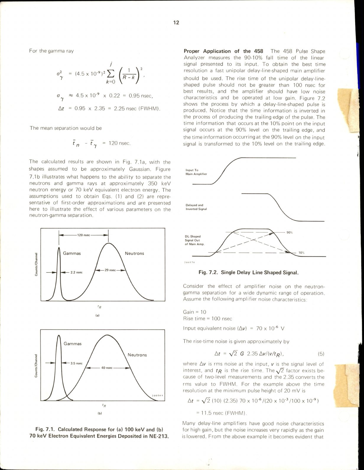
12
For
the
gamma
ray
.
I4,5x.0-'I'E
k=Q
a
4.5
X
10
X
0.22
=
0.95
nsec,
y
At
=
0.95
X
2.35
=
2.25
nsec
(FWHM).
The
mean
separation
would
be
f
„
-
f
y
=
120
nsec.
The
calculated
results
are
shown
in
Fig.
7.1a,
with
the
shapes
assumed
to
be
approximately
Gaussian.
Figure
7.1b
i l
lustrates
what
happens
to
the
abi
lity
to
separate
the
neutrons
and
gamma
rays
at
approximately
350
keV
neutron
energy
or
70
keV
equivalent
electron
energy.
The
assumptions
used
to
obtain
Eqs.
(1)
and
(2)
are
repre
sentative
of
first-order
approximations
and
are
presented
here
to
illustrate
the
effect
of
various
parameters
on
the
neutron-gamma
separation.
Gammas
/
\
Neutrons
—
2.2
nsec
/
J
<a)
Gammas
Neutrons
3.5
nsec
40
nsec
(b)
Fig.
7.1.
Calculated
Response
for
(a)
100
keV
and
(b)
70
keV
Electron
Equivalent
Energies
Deposited
in
NE-213.
L_
Proper
Application
of
the
458
The
458
Pulse
Shape
Analyzer
measures
the
90-10%
fall
time
of
the
l
inear
signal
presented
to
its
input.
To
obtain
the
best
time
resolution
a
fast
unipolar
delay-line-shaped
main
amplifier
should
be
used.
The
rise
time
of
the
unipolar
delay-l
ine-
shaped
pulse
should
not
be
greater
than
100
nsec
for
best
results,
and
the
ampl
ifier
should
have
low
noise
characteristics
and
be
operated
at
low
gain.
Figure
7.2
shows
the
process
by
which
a
delay-line-shaped
pulse
is
produced.
Notice
that
the
time
information
is
inverted
in
the
process
of
producing
the
trai
ling
edge
of
the
pulse.
The
time
information
that
occurs
at
the
10%
point
on
the
input
signal
occurs
at
the
90%
level
on
the
trailing
edge,
and
the
time
information
occurring
at
the
90%
level
on
the
input
signal
is
transformed
to
the
10%
level
on
the
trail
ing
edge.
Input
To
Main
Amplifier
Delayed
and
Inverted
Signal
DL-Shaped
Signal
Out
of
Main
Amp.
Fig.
7.2.
Single
Delay
Line
Shaped
Signal.
Consider
the
effect
of
ampl
ifier
noise
on
the
neutron-
gamma
separation
for
a
wide
dynamic
range
of
operation.
Assume
the
fol
lowing
ampl
ifier
noise
characteristics:
Gain
=
10
Rise
time
=
100
nsec
Input
equivalent
noise
(Av)
=
70
x
10"^
V
The
rise-time
noise
is
given
approximately
by
At
=
yjl
G
2.3bAvl{v/tpi),
(5)
where
Av
is
rms
noise
at
the
input,
v
is
the
signal
level
of
interest,
and
tpt
is
the
rise
time.
The
factor
exists
be
cause
of
two-level
measurements
and
the
2.35
converts
the
rms
value
to
FWHIVl.
For
the
example
above
the
time
resolution
at
the
minimum
pulse
height
of
20
mV
is
At
=
\/2
(10)
(2.35)
70
X
10"®/(20
x
lO'VlOO
x
10"')
=
11.5
nsec
(FWHM).
Many
delay-line
amplifiers
have
good
noise
characteristics
for
high
gain,
but
the
noise
increases
very
rapidly
as
the
gain
is
lowered.
From
the
above
example
it
becomes
evident
that
I

13
the
ampl
ifier
must
be
operated
at
minimum
gain
and
must
have
good
noise
characteristic
before
neutrons
and
gammas
can
be
separated
over
the
entire
ranqe
of
20
mV
to
10
V.
The
ORTEC
460
is
the
only
known
delay-l
ine-shaped
amplifier
with
these
characteristics.
The
458
should
be
operated
in
the
X0.1
V
input
discriminator
range
for
the
400:1
dynamic
range.
In
this
position
1000
divisions
is
equivalent
to
100
mV
at
the
input
to
the
458.
The
458
input
discriminator
control
should
be
set
above
the
input
noise
but
not
lower
than
100
divisions
on
the
control
.
The
setup
procedure
in
Section
3.3
should
be
careful
ly
followed
when
using
the
458
in
the
X0.1
V
range.
In
addition,
the
Walk
Adj
should
be
adjusted
for
optimum
walk
over
the
entire
dynamic
range
of
interest.
-
NEUTRON-GAMMA
DISCRIMINATION
EXPERIMENT
NEUTRON
ENERGY
3
■
0.5
MeV
GAMMA
ENERGY
600
keV
COUNT
RATE
=
25,000
cts/sec.
-
GAMMA
:
^^NEUTRON
—.
A
typical
block
diagram
for
a
neutron—gamma-ray
dis
crimination
system
is
shown
in
Fig.
7.3.
The
458
Pulse
Shape
Analyzer
(PSA)
time
window
is
set
on
the
gamma
peak
and
above
any
extraneous
peaks
in
the
time
spectrum
caused
by
amplitude
saturation
of
the
main
amplifier.
A
UL
logic
pulse
is
generated
for
al
l
events
with
rise
times
greater
than
the
UL
control
setting.
Figure
7.4
is
a
typical
spectrum
of
the
458
output
with
a
plutonium-beryll
ium
source.
ORTEC
456
HIGH
VOLTAGE
POWER
SUPPLY
ORTEC
265
PM
BASE
£
^
ORTEC
ORTEC
z
2
ORTEC
458
113
460
PULSE
SHAPE
PREAMP
AMPLIFIER
ANALYZER
WINDOW
OUTPUT
GAMMA
ROUTING
UL.
OUTPUT
NEUTRON
ROUTING
NEUTRONS
GAMMAS
ENERGY
SIGNAL
Fig.
7.3.
Block
Diagram
for
a
Typical
Neutron-Gamma
Separation
Experiment.
Fig.
7.4.
Neutron-Gamma
Rise
Time
Spectrum.
The
suggested
block
diagram
for
the
proportional
counter
system
for
neutron-gamma
discrimination
is
shown
in
Fig.
7.6.
The
460
delay-line-shaped
ampl
ifier
should
have
a
2-;usec
shaped
line
for
optimum
performance.
The
Lower
Level
control
of
the
window
should
be
set
just
below
the
peak
corresponding
to
the
neutron
rise
time
(see
Fig.
7.5),
and
the
UL
control
should
be
set
just
above
the
neutron
peak.
The
majority
of
the
events
causing
a
window
output
wi
l l
correspond
to
neutrons,
and
the
events
causing
a
UL
output
will
correspond
to
gamma
rays.
NEUTRON
EVENT
GAMMA-RAY
EVENT
RISE
TIME
(Asec)
Fig.
7.5.
A
Typical
Neutron
and
Gamma
Rise
Time
Spectrum
from
a
Proton
Recoil
Proportional
Counter.
7.2.
NEUTRON-GAMMA-RAY
DISCRIMINATION
IN
PROPORTIONAL
COUNTERS
Gamma-ray
discrimination
in
proton-recoi
l
proportional
counters
has
been
accomplished
by
several
experimenters.''
Recently
Dbu'
reported
excel
lent
separation
of
neutrons
and
gammas
at
energies
of
10
keV
and
lower.
The
basic
principle
is
that
the
proton
recoi
ls
from
the
neutrons
produce
a
very
short
ionization
path,
whereas
the
electrons
produced
by
the
gammas
wil
l
occur
over
a
relatively
long
path
in
the
chamber.
Thus
the
rise
time
associated
with
the
neutrons
wi
ll
be
less
than
and
also
better
defined
than
the
rise
time
of
the
gamma
event.
This
is
il
lustrated
in
Fig.
7.5.
ORTEC
459
ORTEC ORTEC
Z
D
ORTEC
HIGH
109
PC
460
458
VOLTAGE
PULSE
SHAPE
POWER
PREAMP
AMPLIFIER
ANALYZER
SUPPLY
PROPOR-
TIONAL
ORTEC
427A
DELAY
AMPLIFIER
WINDOW
OUTPUT
NEUTRON
ROUTING
U.L.
OUTPUT
GAMMA
ROUTING
LINEAR
INPUT
Fig.
7.6.
Neutron-Gamma
Discrimination
System
with
Proportional
Counter.

14
7.3.
RISE-TIME
DISCRIMINATION
IN
X-RAY
PROPORTIONAL
COUNTER
Several
experimenters
have
demonstrated
the
abil
ity
to
distinguish
between
soft
x-rays
and
signals
producing
Compton
electrons
by
observing
the
difference
in
the
2-Msec
SHAPING
8-(.isec
TIME
RANGE
rise
time
of
the
generated
signals.
10-13
Lewyn
in
a
recent
publ
ication
attributed
the
major
portion
of
background
in
proportional
counters
to
high-energy
charged
particles
and
to
Compton
electrons
from
gamma
rays
interacting
with
chamber
wal
ls.
Both
sources
of
background
are
reported
to
have
significantly
longer
col
lection
times
than
soft
x-rays.
A
system
for
distinguishing
between
the
x-ray
events
and
the
non-x-ray
background
is
shown
in
Fig.
7.7.
To
set
the
system
shown
in
Fig.
7.7
the
pulse
shape
distribution
of
2
lisec
SHAPING
ORTEC
459
HIGH
VOLTAGE
POWER
SUPPLY
ORTEC
109PC
PREAMP
ORTEC
451
AMPLIFIER
ORTEC
458
PULSE
SHAPE
ANALYZER
WINDOW
OUTPUT
PROPOR
TIONAL
COUNTER
ORTEC
427A
DELAY
AMPLIFIER
LINEAR
INPUT
MCA
Fig.
7.7.
Background
Reduction
System
for
an
X-Ray
Proportional
Counter.
the
x-rays
and
the
background
must
be
determined.
Once
the
distribution
of
pulse
shapes
is
known,
the
PSA
window
of
the
458
can
be
properly
adjusted.
The
suggested
system
for
setting
the
PSA
window
is
shown
in
Fig.
7.8.
In
this
system
the
pulse
shape
spectrum
should
first
be
accumulated
from
the
458
by
exposing
an
x-ray
source
to
the
chamber
with
the
MCA
in
the
nongated
mode.
The
x-ray
pulse
shape
spectrum
should
be
stored
in
one-half
of
the
memory,
and
then
in
the
second
half
of
the
memory
a
pulse
shape
spectrum
should
be
accumulated
by
exposing
a
gamma-ray
source
(^°Co)
to
the
chamber
with
the
MCA
still
In
the
ungated
mode.
If
the
two
spectra
can
be
overlapped,
a
spectrum
such
as
that
shown
in
Fig.
7.9
should
result.
At
this
point
the
decision
must
be
made
on
where
to
set
the
ORTEC
459
ORTEC ORTEC
ORTEC
HIGH
109
PC
451
458
VOLTAGE
PULSE
SHAPE
POWER
PREAMP
AMPLIFIER
ANALYZER
SUPPLY
PROPOR
TIONAL
WINDOW
OUTPUT
GATE
INPUT
'
4.INEAR
INPUT
Fig.
7.8.
Suggested
System
for
Setting
the
PSA
Window
of
the
458.
BACKGROUND
4
Msec
I
8
Msec
I
Fig.
7.9.
Pulse
Shape
Spectrum
Taken
with
Proportional
Counter
System
Shown
in
Fig.
7.8.
PSA
window.
The
Lower
Level
control
should
clearly
be
set
between
the
lowest
peak
and
the
x-ray
peak.
The
Upper
Level
control
then
must
be
set
somewhere
be
tween
the
x-ray
peak
and
the
background
peak.
The
background
efficiency
rejection
can
never
be
100%;
so
other
parameters
of
the
experiment
should
dictate
how
much
of
the
background
to
reject
with
some
sacrifice
of
x-ray
counting
efficiency.
After
the
decision
is
made
as
to
what
point
on
the
pulse
shape
spectrum
the
window
should
set,
the
MCA
should
display
the
unfolded
x-ray
pulse
shape
spectrum.
Place
the
MCA
in
the
gated
mode
and
expose
the
x-ray
source
to
the
chamber.
The
lower
level
and
upper
level
controls
can
now
be
adjusted
to
preselected
points
in
the
spectrum
by
observing
the
minimum
channel
and
maximum
channel
being
stored
in
the
analyzer.
Once
the
PSA
window
is
set,
the
gated
energy
spectrum
(Fig.
7.7)
can
be
taken.
Table of contents
Other EG&G Measuring Instrument manuals


