ElevATE Semiconductor Whitney User manual

Whitney EVM Guide Rev A: 10/14/2022
Copyright ©Elevate Semiconductor Page 1 of 39
Whitney EVM Guide
Rev A: October 14, 2022
This document contains information on a product under development. The parametric information contains target
parameters that are subject to change.

Whitney EVM Guide Rev A: 10/14/2022
Copyright ©Elevate Semiconductor Page 2 of 39
Document Revision History
Revision
Date
Description
A
10/14/2022
Initial Draft.
Table of Contents
1INTRODUCTION..................................................................................................................................... 5
2EVM GUI INSTALLATION MEDIA............................................................................................................. 6
2.1 Software Installation..............................................................................................................................................................6
2.2 Support Files ..........................................................................................................................................................................8
3WARNINGS............................................................................................................................................ 9
4HARDWARE......................................................................................................................................... 10
4.1 Power Supplies ....................................................................................................................................................................10
4.2 EVM USB Cable ....................................................................................................................................................................11
4.3 External Hardware Required for GPIB Use ...........................................................................................................................11
5GUI OVERVIEW.................................................................................................................................... 12
5.1 Starting the GUI ...................................................................................................................................................................12
5.2 Powering up the Whitney Device .........................................................................................................................................13
5.3 Channel 0 Register Map Display After Loading Default Register Settings .............................................................................13
5.4 Loading Calibration Factors..................................................................................................................................................14
5.5 Editing Registers ..................................................................................................................................................................14
6INITIAL DEFAULT CHANNEL 0 FORCE VOLTAGE SETTINGS ..................................................................... 15
7MODIFYING VRNG AND VCNTR............................................................................................................ 16
8DIGITAL RAMP FUNCTION ................................................................................................................... 16
9WHITNEY DAC NON-LINEARITY AND FORCE VOLTAGE ACCURACY ........................................................ 17
10 SUGGESTED VCNTR AND VRNG SETTINGS FOR TYPICAL SUPPLY VOLTAGE RANGES .............................. 18
11 OPTIONAL CONTROL: OPEN AND CLOSE EVM RELAYS .......................................................................... 19
12 MEASURE VOLTAGE............................................................................................................................. 20
13 CALIBRATION ...................................................................................................................................... 21
13.1 Manual Calibration of Whitney EVM....................................................................................................................................21
13.2 Verifying DAC Calibration Accuracy –Uncalibrated DAC ......................................................................................................22
13.3 Verifying FV_A DAC Calibration Accuracy.............................................................................................................................23
13.4 Verifying FV and MV Calibration Accuracy ...........................................................................................................................24
13.5 Verifying FI and MI Calibration Accuracy..............................................................................................................................25
14 CONNECT MON_A_0 (CH0 MONITOR OUTPUT) TO SMA CONNECTOR J20 ............................................ 26
15 FORCE VOLTAGE SLEW RATE CONTROL AND MEASURE CURRENT MONITORING .................................. 27
15.1 Step 1: FV Slew Rate and MI Monitoring..............................................................................................................................27
15.2 Step 2: FV Slew Rate and MI Monitoring..............................................................................................................................28
16 AUTOMATIC VS. MANUAL SELECTION OF COMPENSATION AND FF CAPS ............................................. 29

Whitney EVM Guide Rev A: 10/14/2022
Copyright ©Elevate Semiconductor Page 3 of 39
17 FORCE CURRENT SLEW RATE CONTROL AND MEASURE CURRENT MONITORING .................................. 30
17.1 Step 1: FI Slew Rate Control and MI Monitoring...................................................................................................................30
17.2 Step 2: FI Slew Rate Control and MI Monitoring...................................................................................................................31
17.3 Step 3: FI Slew Rate Control and MI Monitoring...................................................................................................................32
18 ENABLING AND SETTING ACCURATE VOLTAGE CLAMPS ....................................................................... 33
18.1 Step 1: Enabling and Setting Accurate Voltage Clamps.........................................................................................................33
18.2 Step 2: Enabling and Setting Accurate Voltage Clamps.........................................................................................................34
19 ENABLING AND SETTING ACCURATE CURRENT CLAMPS ....................................................................... 35
19.1 Step 1: Enabling and Setting Accurate Current Clamps.........................................................................................................35
19.2 Step 2: Enabling and Setting Accurate Current Clamps.........................................................................................................36
20 FORCE VOLTAGE GANGING AND MEASURE CURRENT MONITORING .................................................... 37
20.1 Step 1: FV Ganging and MI Monitoring.................................................................................................................................37
20.2 Step 2: FV Ganging and MI Monitoring.................................................................................................................................37
20.3 Step 3: FV Ganging and MI Monitoring.................................................................................................................................38
20.4 Step 4: FV Ganging and MI Monitoring.................................................................................................................................38
21 MEASURING DIE TEMPERATURE.......................................................................................................... 39
22 EXPERIMENTING WITH HIGHER SUPPLY VOLTAGES.............................................................................. 39
23 CONCLUSION....................................................................................................................................... 39
23.1 Additional Support...............................................................................................................................................................39

Whitney EVM Guide Rev A: 10/14/2022
Copyright ©Elevate Semiconductor Page 4 of 39
Table of Tables
TABLE 1: RECOMMENDED DIODE LOCATIONS FOR THE BAS70SW-AU_R1_000A1...................................................................................9
TABLE 2: VCNTR AND VRNG.....................................................................................................................................................................18
TABLE 3: RECOMMENDED COMP AND FF CAPS ......................................................................................................................................29
Table of Figures
FIGURE 1: EVM AND DIGITAL CONTROLLER BOARD .................................................................................................................................5
FIGURE 2: INSTALLER DIRECTORY .............................................................................................................................................................6
FIGURE 3: INSTALLATION DIRECTORY.......................................................................................................................................................6
FIGURE 4: GUI DIRECTORY ........................................................................................................................................................................7
FIGURE 5: GUI INSTALLATION ...................................................................................................................................................................7
FIGURE 6: SUPPORT FILES .........................................................................................................................................................................8
FIGURE 7: EVM POWER SUPPLY BANANA JACKS ....................................................................................................................................10
FIGURE 8: MICRO-USB CONNECTOR.......................................................................................................................................................11
FIGURE 9: GUI STARTUP..........................................................................................................................................................................12
FIGURE 10: POWER UP............................................................................................................................................................................13
FIGURE 11: DEFAULT REGISTER MAP......................................................................................................................................................13
FIGURE 12: LOADING CALIBRATION FILES...............................................................................................................................................14
FIGURE 13: REGISTER BITS ......................................................................................................................................................................14
FIGURE 14: ENABLE/DISABLE CHANNELS................................................................................................................................................15
FIGURE 15: CHANNEL CONNECT .............................................................................................................................................................15
FIGURE 16: FV RAMP...............................................................................................................................................................................16
FIGURE 17: UNCALIBRATED DAC.............................................................................................................................................................17
FIGURE 18: CALIBRATED DAC..................................................................................................................................................................17
FIGURE 19: EVM RELAYS .........................................................................................................................................................................19
FIGURE 20: MEASURE VOLTAGE .............................................................................................................................................................20
FIGURE 21: CALIBRATION........................................................................................................................................................................21
FIGURE 22: DAC VERIFICATION UNCALIBRATED .....................................................................................................................................22
FIGURE 23: DAC CALIBRATION VERIFICATION ........................................................................................................................................23
FIGURE 24: FV AND MV VERIFICATION ...................................................................................................................................................24
FIGURE 25: FI AND MI CALIBRATION VERIFICATION...............................................................................................................................25
FIGURE 26: CONNECT MON_A_0 TO SMA ..............................................................................................................................................26
FIGURE 27: FV RAMP STEP SIZE 8............................................................................................................................................................27
FIGURE 28: FV RAMP STEP SIZE 6............................................................................................................................................................27
FIGURE 29: FV RAMP REGISTER BITS ......................................................................................................................................................28
FIGURE 30: COMPENSATION CAPACITOR ...............................................................................................................................................29
FIGURE 31: FI SLEW RATE CONTROL AND MI MONITORING ..................................................................................................................30
FIGURE 32: FEED FORWARD CAPACITOR 100NF.....................................................................................................................................31
FIGURE 33: FEED FORWARD CAPACITOR 1μF .........................................................................................................................................31
FIGURE 34: REGISTER BITS FI RAMP........................................................................................................................................................32
FIGURE 35: VOLTAGE CLAMPS ................................................................................................................................................................33
FIGURE 36: RISING FORCE CURRENT.......................................................................................................................................................34
FIGURE 37: FALLING FORCE CURRENT ....................................................................................................................................................34
FIGURE 38: GUI CURRENT CLAMP CONTROL ..........................................................................................................................................35
FIGURE 39: RISING FV .............................................................................................................................................................................36
FIGURE 40: FALLING FV ...........................................................................................................................................................................36
FIGURE 41: FV GANGING AND MI MONITORING STEP 1 ........................................................................................................................37
FIGURE 42: FV GANGING AND MI MONITORING STEP 2 ........................................................................................................................37
FIGURE 43: FV GANGING AND MI MONITORING STEP 3 ........................................................................................................................38
FIGURE 44: FV GANGING AND MI MONITORING STEP 4 ........................................................................................................................38
FIGURE 45: MEASURE TEMP ...................................................................................................................................................................39
Whitney EVM Guide Rev A: 10/14/2022
Copyright ©Elevate Semiconductor Page 5 of 39
1Introduction
Congratulations on your purchase of an Elevate Semiconductor Whitney evaluation system! You will find that it serves as an
invaluable development platform to help get your product to market in the shortest possible time. The Whitney evaluation
board and GUI (Graphical User Interface) allow the customer to demonstrate and evaluate Whitney performance and
functionality.
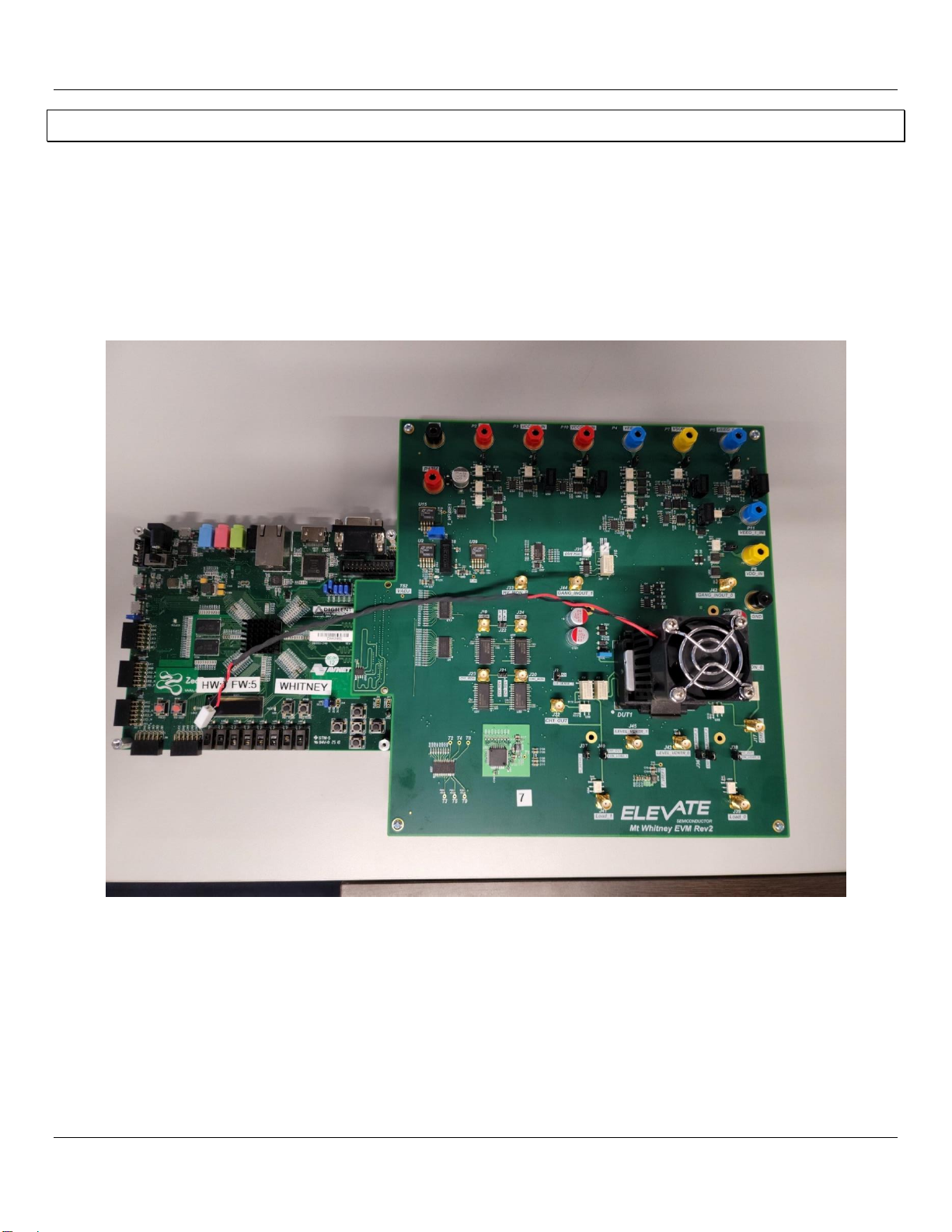
The Whitney EVM and digital controller board with USB interface are mounted to a baseboard. For detailed assembly
instructions, please see the Elevate Whitney Setup Video.
FIGURE 1: EVM AND DIGITAL CONTROLLER BOARD
Whitney EVM Guide Rev A: 10/14/2022
Copyright ©Elevate Semiconductor Page 6 of 39
2EVM GUI Installation Media
The Whitney EVM ships with self-installing software on the included flash drive. To ensure the evaluation board is correctly
recognized when connected to the PC, the software should be installed before connecting the board to the Evaluation PC’s
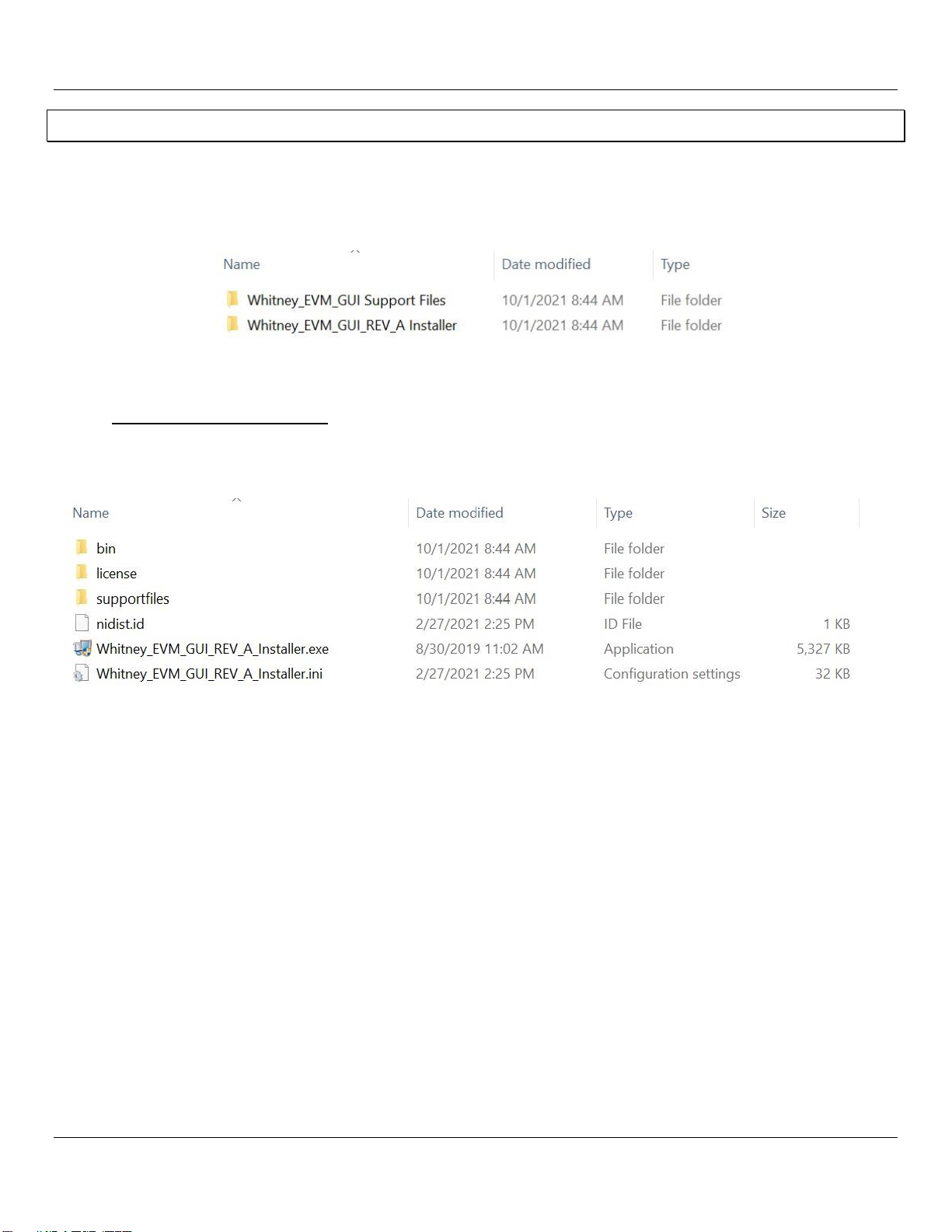
USB port. The installation media (flash drive) includes the Installer directory, and a directory with support files and the most
recent version of the Whitney EVM GUI.
FIGURE 2: INSTALLER DIRECTORY
2.1 Software Installation
To begin the installation of the EVM GUI, open the “Whitney_EVM_GUI_REV_A Installer”directory and double-click on
“Whitney_EVM_GUI_REV_A_Installer.exe”.
FIGURE 3: INSTALLATION DIRECTORY
Whitney EVM Guide Rev A: 10/14/2022
Copyright ©Elevate Semiconductor Page 7 of 39
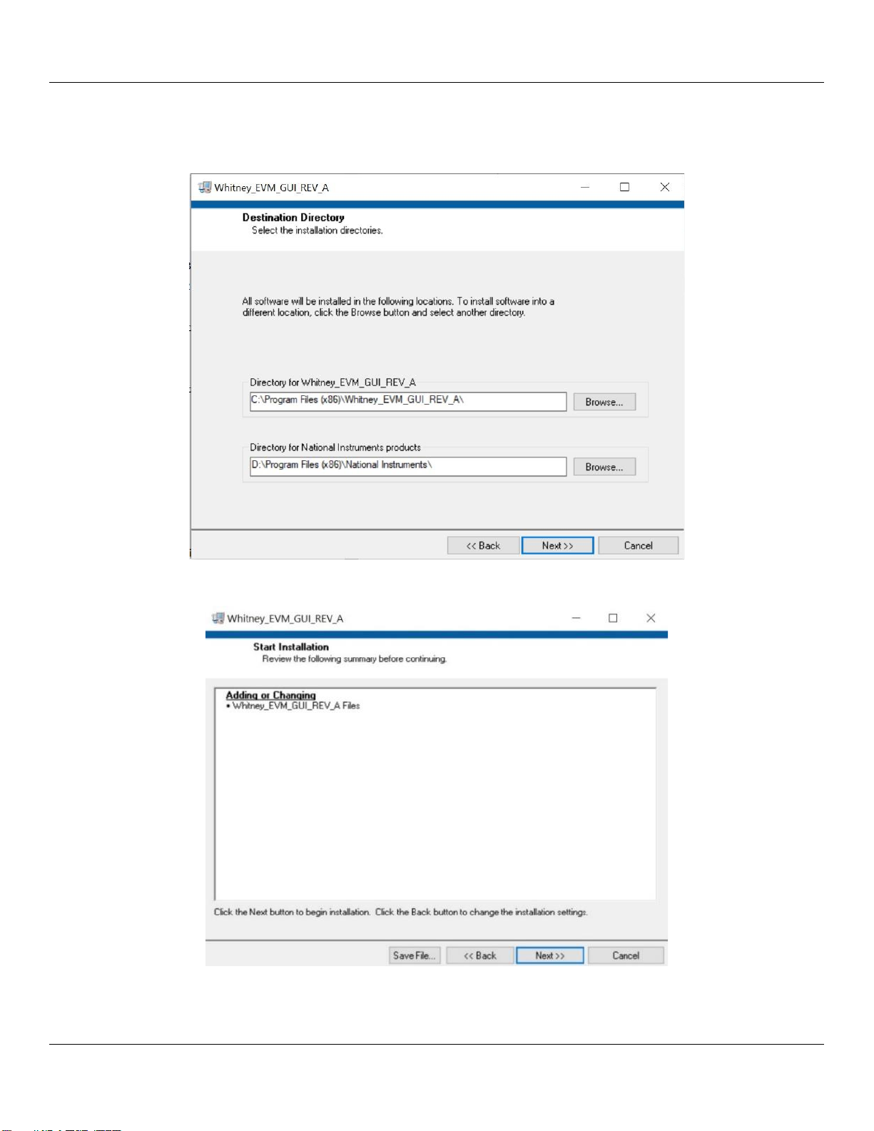
The default installation directory is “C:\Program Files(x86)\Whitney_EVM_GUI_REV_A”. However, the EVM GUI can be installed
to any directory on any drive where the user has full rights to read, write, and modify files. Click Next to begin installation.
FIGURE 4: GUI DIRECTORY
FIGURE 5: GUI INSTALLATION
Whitney EVM Guide Rev A: 10/14/2022
Copyright ©Elevate Semiconductor Page 8 of 39
2.2 Support Files
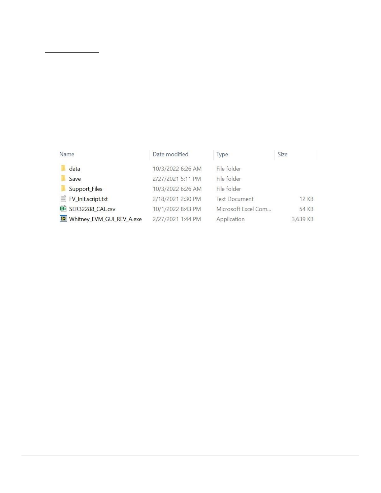
Following installation, you will be asked to re-boot your computer. After re-booting, navigate to the directory where
“Whitney_EVM_GUI_REV_A.exe”has been installed, and copy the files from the “Whitney_EVM_GUI Support Files”directory on
the installation media into the same directory. The directory should now contain the files shown below, although there may be
additional “SERxxxxx_CAL.csv” files. If you have been provided with additional SERxxxxx_CAL.csv files, copy the files into this
directory.
The ”Whitney_EVM_GUI Support Files” directory will also include a more recent revision of the Whitney EVM GUI. Copy this
revision (Whitney_EVM_GUI_REV_x.exe) into this directory and delete Whitney_EVM_GUI_REV_A.exe.
FIGURE 6: SUPPORT FILES
Whitney EVM Guide Rev A: 10/14/2022
Copyright ©Elevate Semiconductor Page 9 of 39
3Warnings
Whitney is a high voltage part with the ability to source significantly over 200mA of current. Special care must be taken when
using this product to ensure the safety of the device, board, and user. Please read the following cautions carefully and make
sure that the hardware and software comply with the restrictions listed. Failure to adhere to the restrictions below can result
in severe damage to the device. Users must read the datasheet and quick start guide thoroughly. In the event of confusion or
uncertainty please reach out to the Elevate Applications Team for guidance. For REVB Silicon see the errata for additional
warnings and clarifications.
1) Power supply order MUST be followed exactly. Allow minimum 5mS between supplies. The power up order and minimum
time sequence is by default, adhered to by the Whitney EVM power on sequence.
2) Output may NEVER go below VEEO.
3) VSUB must ALWAYS be the lowest supply in the system (as low as VEEO or VEE, whichever is lower).
4) The clamps CANNOT be engaged if the output is already over the clamp limit. Clamps should be set when the part is not
outputting (HiZ).
5) Clamps will NOT prevent damage to the Whitney device from an external source, clamps will only limit what the chip itself
will try to output. Do not use clamps to limit external current or voltage.
6) Fast transient voltages or currents can damage the output due to a large mismatch between internal and external nodes.
Settling time may be needed (or a discharge path) to ensure that there is not a large difference between internal and
external voltages.
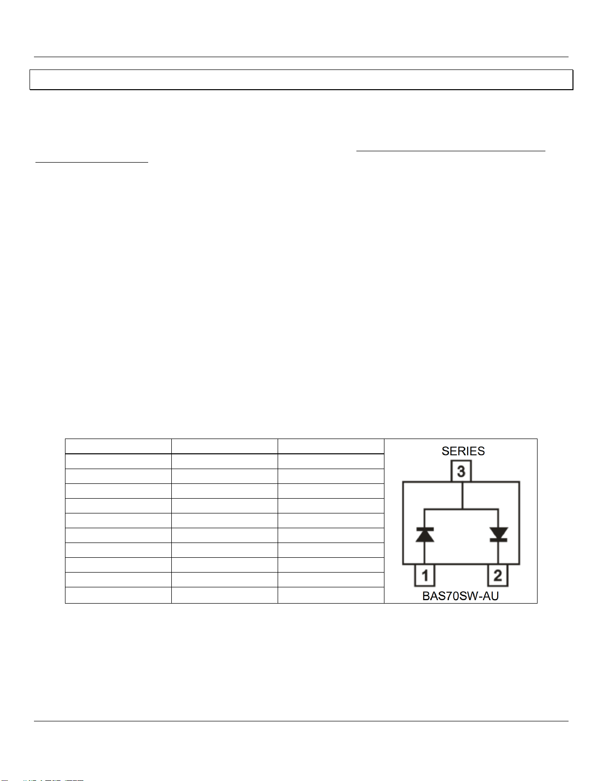
External Schottky diodes (Elevate recommends something like the BAS70SW-AU_R1_000A1) on high voltage pins may help
reduce the possibility of transients or out-of-compliance voltages from damaging the Whitney device and should be
considered in design. These diodes are already installed on the Whitney EVM. If using these specific diodes, below is the way
the 3 pins should be set up for best protection:
TABLE 1: RECOMMENDED DIODE LOCATIONS FOR THE BAS70SW-AU_R1_000A1
Pin 1 (Left)
Pin 2 (right)
Pin 3 (top)
VEEO_0
VCCO_0
Force0_0 (pin 56, 57)
VEEO_0
VCCO_0
Force1_0 (pin 45)
VEEO_0
VCCO_0
HI_Sense_0 (pin 43)
VSUB
VCCO_0
Lo_Sense_0 (pin 41)
VSUB
VCCO_0
HV_Mon_0 (pin 64)
VSUB
VCCO_1
Lo_Sense_1 (pin 126)
VSUB
VCCO_1
HV_Mon_1 (pin 103)
VEEO_1
VCCO_1
Force0_1 (pin 110,111)
VEEO_1
VCCO_1
Force1_1 (pin 122)
VEEO_1
VCCO_1
HI_Sense_1 (pin 124)

Whitney EVM Guide Rev A: 10/14/2022
Copyright ©Elevate Semiconductor Page 10 of 39
4Hardware
4.1 Power Supplies
The following power supply settings are a safe condition selected when the Whitney EVM is initially powered up but any rails
within the valid operating condition can be powered up to:
1. Common ground return for all supplies (Black Banana jack labeled GND)
2. Whitney VDD and VDDA (+1.8V @ 25mA MAX, Yellow Banana jack labeled VDD)
3. Whitney VCC (+2.75V @ 70mA MAX, Red Banana jack labeled VCC)
4. Whitney VEE (-2.75V @ 95mA MAX, Blue Banana jack labeled VEE)
5. +12V @ 1A (Red Banana Jack labeled +12V, also powers ZED board)
6. Whitney CH1 VEEO (-5V @ 1A MAX, Blue banana jack labeled VEEO_1)
7. Whitney CH0 VEEO (-5V @ 1A MAX, Blue banana jack labeled VEEO_0)
8. Whitney CH1 VCCO (+10V @ 1A MAX, Red banana jack labeled VCCO_1)
9. Whitney CH0 VCCO (+10V @ 1A MAX, Red banana jack labeled VCCO_0)
10. Whitney VSUB (-5V @ 10mA MAX VSUB supply, Yellow banana jack labeled VSUB)
Note: VSUB must always be the most negative supply. Although VEEO can be more positive than VSUB, during initial
evaluation this absolute requirement is most easily met by powering VSUB, VEEO_0, and VEEO_1 from the same -5V supply.
FIGURE 7: EVM POWER SUPPLY BANANA JACKS
Whitney EVM Guide Rev A: 10/14/2022
Copyright ©Elevate Semiconductor Page 11 of 39
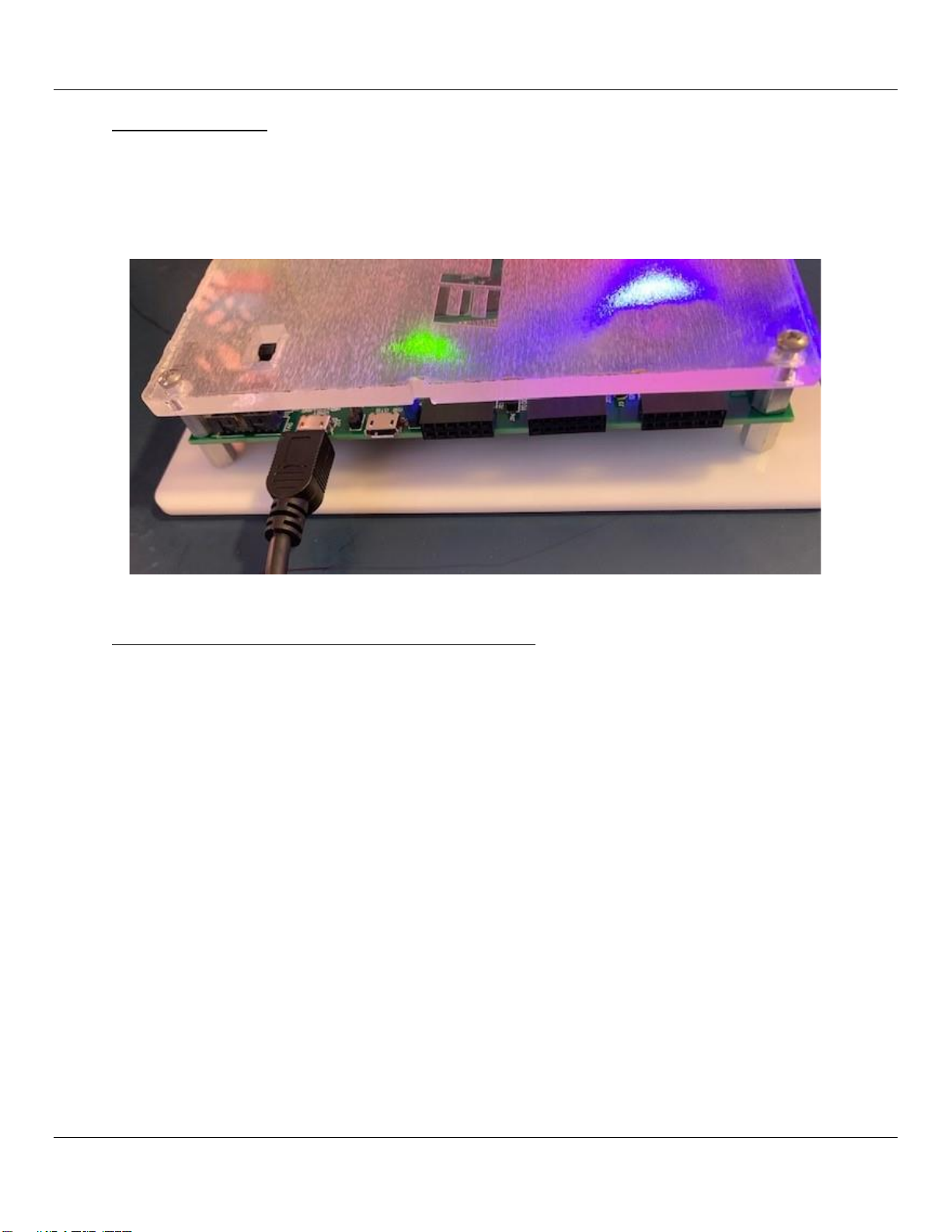
4.2 EVM USB Cable
Plug the USB type-A connector of the included USB cable into your computer and carefully plug the Micro-USB connector into
the EVM connector UART (J14) as shown below.
Caution: The UART USB connector is soldered to the PCB with small surface mount pads and can be damaged or completely
detached from the EVM if the USB cable is accidentally pulled up, down, or sideways.
FIGURE 8: MICRO-USB CONNECTOR
4.3 External Hardware Required for GPIB Use
In order to run the Whitney EVM with the GPIB enabled, you are required to have connected:
•3 BK Precision 9132B- Triple Output Programable DC Power Supplies (for controlling the supplies)
•1 Agilent 34401A Digital Multimeter (for voltage calibration)
•1 Keithley 238 High Current Source Measure Unit (for the current calibration)
A subset of these instruments cannot be used. It is all or nothing.

Whitney EVM Guide Rev A: 10/14/2022
Copyright ©Elevate Semiconductor Page 12 of 39
5GUI Overview
5.1 Starting the GUI
The external supplies should be enabled prior to starting the GUI (the digital controller board is powered from the external
+12V supply). Double click on “Whitney_EVM_GUI_REV_[A..Z].exe” to start the GUI. The Whitney EVM GUI initial default display:
GPIB is disabled by default and may not be used unless the instruments in section 4.3 are connected.
FIGURE 9: GUI STARTUP
Whitney EVM Guide Rev A: 10/14/2022
Copyright ©Elevate Semiconductor Page 13 of 39
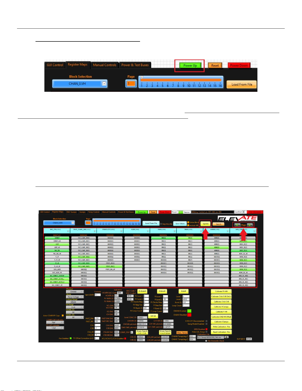
5.2 Powering up the Whitney Device
Click on the green “Power Up” button to apply power to the Whitney device:
FIGURE 10: POWER UP
Power supply currents should be checked from the front of the power supplies. Please make sure current limits are set as to
not cause excessive damage to the EVM in the event of a failure before power up. Whitney EVM initial power supply current
(typical values):
IDD (+1.8V): 38mA
VCC (+2.75V): 14mA
VEE (-2.75V): -24mA
VCCO_0 (+10V): 9mA
VCCO_1 (+10V): 9mA
VEEO_0 (-5V): 1mA
VEEO_1 (-5V): 1mA
VSUB (-5V): 13mA
+12V: 600mA
5.3 Channel 0 Register Map Display After Loading Default Register Settings
The default register settings select Voltage Range 0 (VRNG0) and the 2mA current range (IRNG3). Click on the yellow Update
button to update the display. Click on the Page left arrow or Page right arrow to scroll horizontally through the Register Map.
FIGURE 11:DEFAULT REGISTER MAP
Whitney EVM Guide Rev A: 10/14/2022
Copyright ©Elevate Semiconductor Page 14 of 39
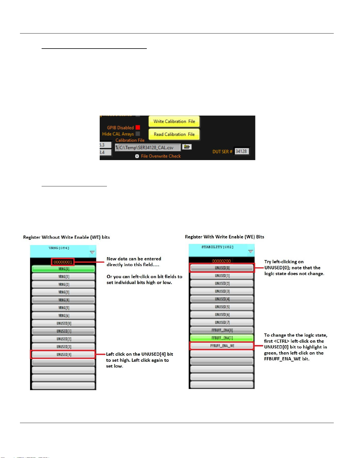
5.4 Loading Calibration Factors
Each EVM has a unique set of calibration factors optimized for the Whitney device that was shipped with the EVM. These
calibration factors are contained in a file with the name format “SERxxxxx_CAL.csv”, where “xxxxx” is the serial number of the
Whitney device shipped with the EVM. The unique Whitney serial number is read from a device register and is displayed as an
integer in the lower right-hand corner of the GUI display called “DUT SER #”. If the incorrect calibration factors are loaded or
the part is not calibrated, the voltages and currents forced and measured by the EVM will be less accurate. The calibration
files are read-only to prevent them from being accidentally over-written. You may find it convenient to copy the
“SER_xxxxx_CAL.csv” calibration file associated with your EVM to “c:\temp\”. Type the Calibration File name and click the
“Read Calibration File” button to load the correct calibration factors for your EVM.
FIGURE 12:LOADING CALIBRATION FILES
5.5 Editing Registers
A bit highlighted in green is a logic high; a bit that is not highlighted is a logic low. Experiment with editing the VRNG and
STABILITY registers. All changes are immediately written to the device in real time (there is no risk of damage to the Whitney
device at this point as both channels are disabled). The contents of the VRNG and STABILITY registers will be updated
automatically whenever the Whitney voltage or current ranges are changed from the GUI front panel. There are two different
types of registers, one with write enables and one without; see below to use the two types of registers.
FIGURE 13: REGISTER BITS

Whitney EVM Guide Rev A: 10/14/2022
Copyright ©Elevate Semiconductor Page 15 of 39
6Initial Default Channel 0 Force Voltage Settings
Connect a voltmeter to Whitney PMU Channel 0 output (SMA connector J17, silkscreen label CHAN0_OUT) and click on the red
CHAN0 Disabled button. The button color will change from red to green, and the text will be updated to CHAN0 Enabled. The
voltmeter should now read +2.00V.
FIGURE 14:ENABLE/DISABLE CHANNELS
Click on the yellow Update button. Note that the PMU_CFG register bit CONNECT has changed state from a logic low to a logic
high (the CONNECT register bit text box is now highlighted in green). The GUI updated this register bit when you clicked on the
red CHAN0 Disabled button.
FIGURE 15:CHANNEL CONNECT
Whitney EVM Guide Rev A: 10/14/2022
Copyright ©Elevate Semiconductor Page 16 of 39
7Modifying VRNG and VCNTR
The minimum and maximum Force Voltage and Measure Voltage for the VRNG are calculated by LabView and indicated by FV
VMIN (V) and FV VMAX (V). The Force Voltage and Measure Voltage range can be shifted up or down by entering a new value
into the Set VCNTR control and pressing <Enter>; LabView will calculate the required digital offset and update the VCNTR DAC
register and the VCNTR DAC Code indicator. See the datasheet for how to manually calculate the voltage output based on your
VCNTR. If you have a Revision B parts, see the Errata as well.
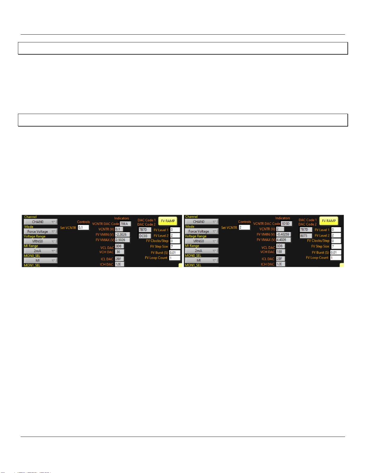
8Digital Ramp Function
Whenever the “FV RAMP” button is clicked, the DAC Code 1 and DAC Code 2 indicators are updated to reflect the voltage
levels set by controls FV Level 1 and FV Level 2. Note that with Set VCNTR = 0.1, DAC Code 2 is 0xDC03. Change Set VCNTR to
2(+2V) and press <Enter>; FV VMIN (V) is updated from -2.3026 to -0.40259, FV VMAX (V) is updated from 2.5026 to 4.4026,
VCNTR DAC Code is updated from 0x78EA to 0x1D5D, and DAC Code 2 is now 0x8073 (actual FV and VCNTR DAC codes will
vary from device to device, depending on the Force Voltage gain and offset). Note that the voltmeter reading is unchanged at
+2.000V; when you modified VCNTR, the LabView code automatically updated Whitney registers to maintain the voltage set
by FV Level 2. Return Set VCNTR to 0.1 and press <Enter> before proceeding to the next step.
Note that with Set VCNTR = 0.1, DAC Code 2 value displayed in Figure 16 is 0xDC03 (actual DAC codes will vary from device to
device)
FIGURE 16:FV RAMP
Whitney EVM Guide Rev A: 10/14/2022
Copyright ©Elevate Semiconductor Page 17 of 39
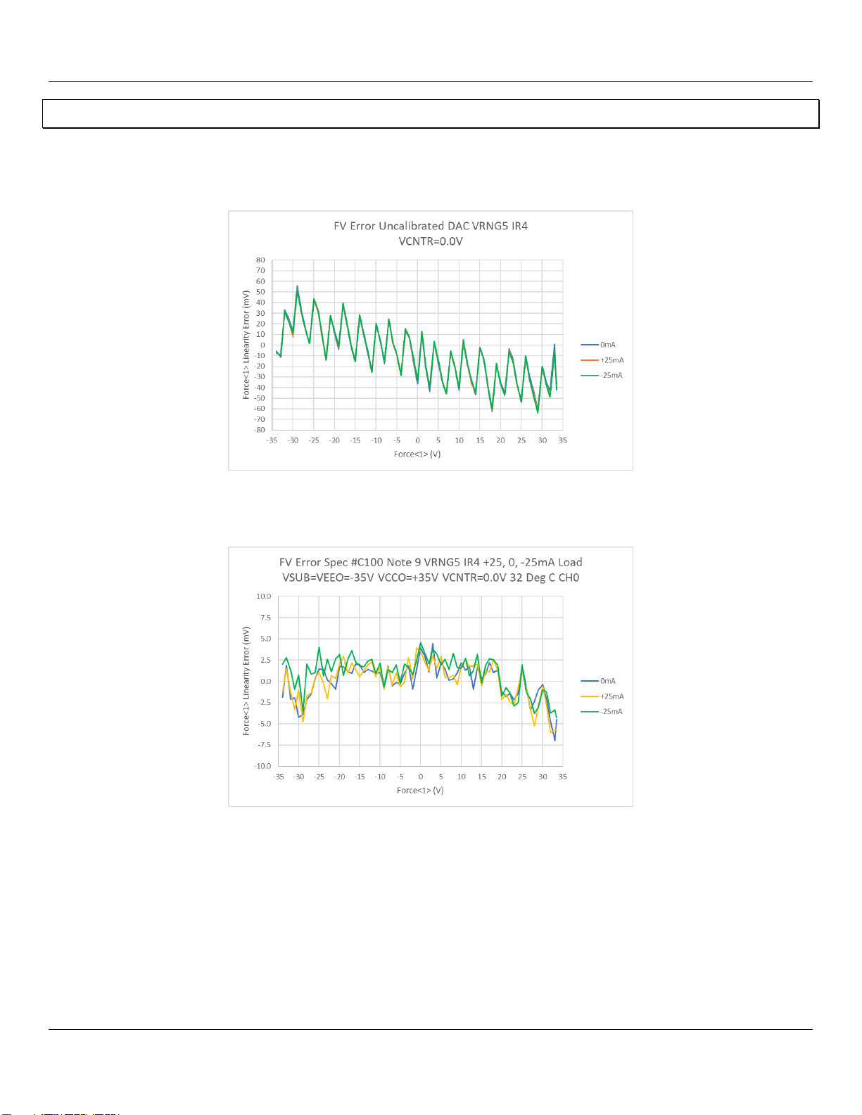
9Whitney DAC Non-Linearity and Force Voltage Accuracy
The Whitney 16-bit DACs are non-monotonic and require a multi-point calibration to achieve the specified Force Voltage
accuracy. The Whitney GUI implements a full multi-point DAC calibration. Note that in Figure 17the scale goes from ± 80mV
but in Figure 18, the scale is from ±10mV
FIGURE 17: UNCALIBRATED DAC
FIGURE 18: CALIBRATED DAC

Whitney EVM Guide Rev A: 10/14/2022
Copyright ©Elevate Semiconductor Page 18 of 39
10 Suggested VCNTR and VRNG Settings for Typical Supply Voltage
Ranges
The internal DACs have a nominal range of -2.4V to +2.4V; in VRNG5 the nominal Force Voltage (FV) and Measure Voltage
(MV) gain is 16.67. Use the lowest possible VRNG setting to minimize output noise and improve FV and MV accuracy and drift
over temperature. The chart below demonstrates how VCNTR can be shifted up or down to maximize the coverage of each
voltage range. The DAC codes shown are for reference only and will vary from channel to channel and device to device.
Note that the FV DAC code is 0x7FFF when Force Voltage = VCNTR; LabView uses the VCNTR DAC to compensate for any Force
Voltage offset.
TABLE 2: VCNTR AND VRNG
VSUB
VEEO
VCCO
VRNG
Usable Range at ±IMAX
Force Voltage
VCNTR
FV DAC Code
VCNTR DAC Code
-6
-6
6
0
VCCO -1.5V
4.5
2.25
0xEC39
0x1361
-6
-6
6
0
((VCCO-VEEO/2)+VEEO
0
0
0x7FFF
0x7F87
-6
-6
6
0
VEEO+1V
-5
-2.5
0x07BF
0xF7B2
-6
-6
7.5
1
VCCO -1.5V
6
3.2
0xF004
0x0405
-6
-6
7.5
1
((VCCO-VEEO/2)+VEEO
0.75
0.75
0x7FFF
0x60CB
-6
-6
7.5
1
VEEO+1V
-5
-2.8
0x2B0A
0xEB4F
-6
-6
13
2
VCCO -1.5V
1.5
5.7
0xF004
0x1182
-6
-6
13
2
((VCCO-VEEO/2)+VEEO
3.5
3.5
0x7FFF
0x3C0B
-6
-6
13
2
VEEO+1V
-5
-2
0x460E
0xA660
-16
-16
16
3
VCCO -1.5V
14.5
7.3
0xEF40
0x0ECE
-16
-16
16
3
((VCCO-VEEO/2)+VEEO
0
0
0x7FFF
0x7FB6
-16
-16
16
3
VEEO+1V
-15
-7.3
0x0904
0xF09E
-30
-30
30
4
VCCO -1.5V
28.5
14.6
0xEB5B
0x0ED5
-30
-30
30
4
((VCCO-VEEO/2)+VEEO
0
0
0x7FFF
0x7FB4
-30
-30
30
4
VEEO+1V
-29
-14.6
0x10C6
0xF093
-5
-5
65
5
VCCO -1.5V
63.5
30
0xE109
0x28B7
-5
-5
65
5
((VCCO-VEEO/2)+VEEO
30
30
0x7FFF
0x28B7
-5
-5
65
5
VEEO+1V
-4
30
0x1D82
0x28B7
-64
-64
6
5
VCCO -1.5V
4.5
-29
0xE109
0xD3C9
-64
-64
6
5
((VCCO-VEEO/2)+VEEO
-29
-29
0x7FFF
0xD3C9
-64
-64
6
5
VEEO+1V
-63
-29
0x1D82
0xD3C9
Whitney EVM Guide Rev A: 10/14/2022
Copyright ©Elevate Semiconductor Page 19 of 39
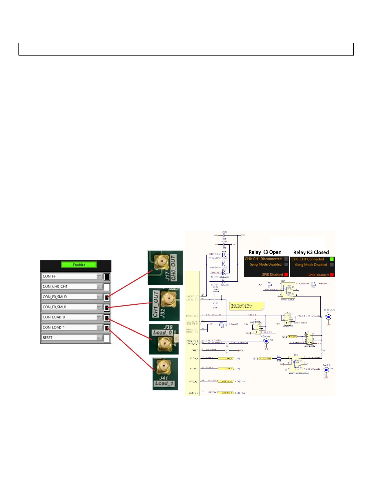
11 Optional control: Open and Close EVM Relays
Navigate to the “Manual Controls” tab (located in the upper left-hand corner). EVM relays can be opened or closed by selecting
or de-selecting a relay name and clicking on the green “Enables” button. Relays are selected or de-selected by clicking on the
box the right of the relay name until the box color changes from black to white (de-selected) or until the color changes from
white to black (selected). The following relays were automatically closed when you clicked on the “Power Up” button:
CON_F0_SMU0: Connects the Whitney FORCE_HI_0 output and SENSE_HI_0 input to the center pin of SMA connector J17.
CON_F0_SMU1: Connects the Whitney FORCE_HI_1 output and SENSE_HI_1 input to the center pin of SMA connector J32.
CON_LOAD_0: Connects the center pin of SMA J39 to the center pin of SMA J17 to allow the controlled connection of external
loads.
CON_LOAD_1: Connects the center pin of SMA J41 to the center pin of SMA J32 to allow the controlled connection of external
loads.
CON_FF: Closes relays K2 and K5 to connect the 100nf and 1μf feed-forward capacitors. Also connects the CH0 and CH1 high
current FORCE_HI_# outputs to the low current FORCE_LI_# outputs. Opening K2 and K5 to disconnect the feed-forward
capacitors in the 2μA and 20μA current ranges allows for faster measure current settling time and will also reduce the HiZ
leakage by a small number of nanoamps. The GUI will open and close relays K2 and K5 automatically depending on the
current range selected.
CON_CH0_CH1: Closes relay K3, connecting FORCE_HI_0 output to FORCE_HI_1. This relay can also be controlled by clicking
on CH0-CH1 Disconnected or CH0-CH1 Connected
FIGURE 19: EVM RELAYS
Whitney EVM Guide Rev A: 10/14/2022
Copyright ©Elevate Semiconductor Page 20 of 39
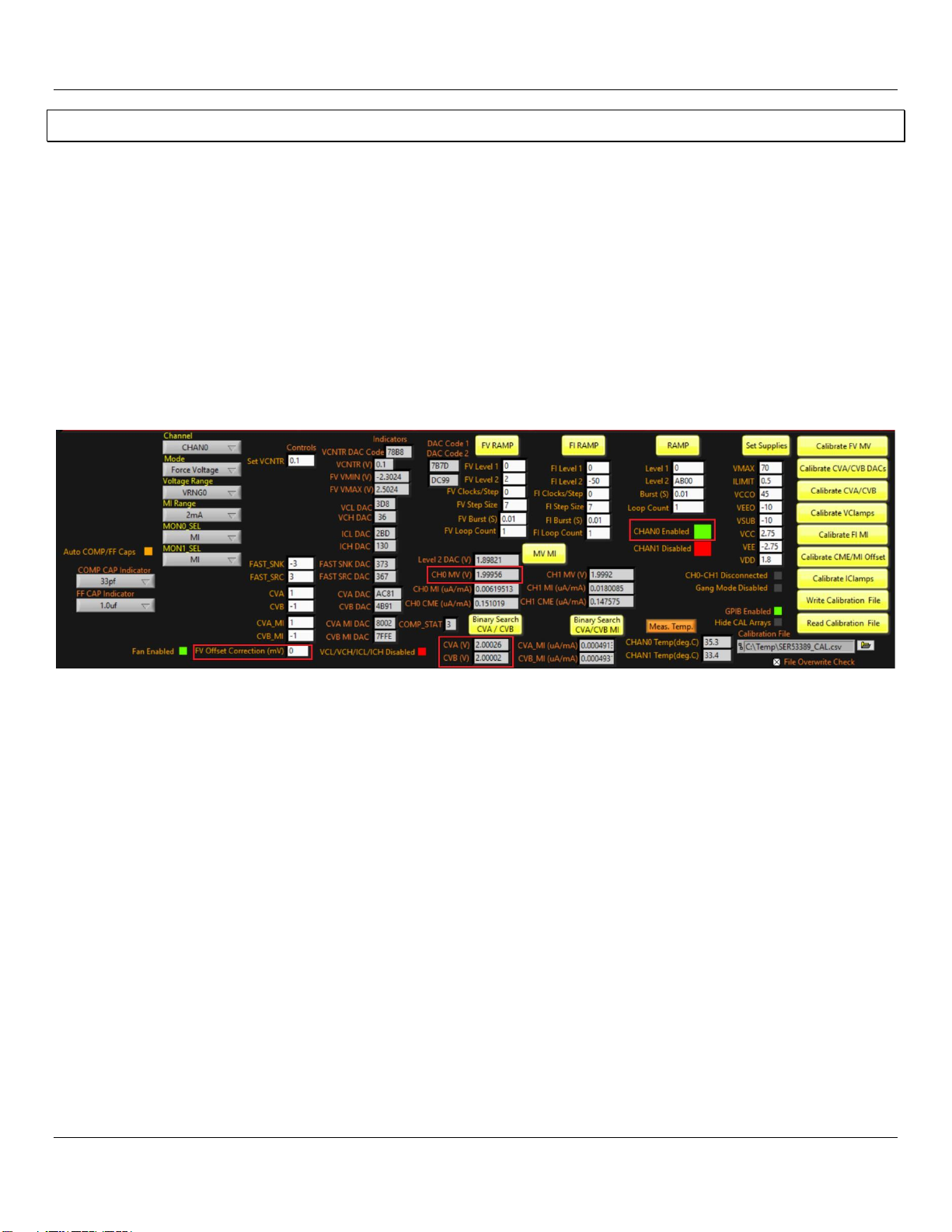
12 Measure Voltage
Navigate back to the “Register Maps” tab (located in the upper left-hand corner). CH0 is enabled; your voltmeter should read
+2.0V.
1. The FV Offset Correction (mV) control can be used to “null out” any residual Force Voltage offset on a per-voltage
range basis. For example, if your voltmeter reads +1.3mV when FV Level 2 is set to 0.0, enter 1.3 into FV Offset
Correction (mV) and press <Enter>. The offset correction will be applied, and you should now read 0.0mV on your
voltmeter.
2. Click the “MV MI” button; the CH0 MV (V) indicator will update to the measured voltage at SENSE_HIGH_0. The CH1
MV (V) indicator will also update to the measured voltage at SENSE_HIGH_1 However, CH1 is not enabled, so the
reading will be invalid.
3. Click on the “Binary Search CVA / CVB” button to perform binary searches of the CVA and CVB comparator thresholds;
the CVA (V) and CVB (V) indicators will be updated accordingly and should read the same as the external DMM.
FIGURE 20:MEASURE VOLTAGE
Table of contents
Other ElevATE Semiconductor Motherboard manuals


