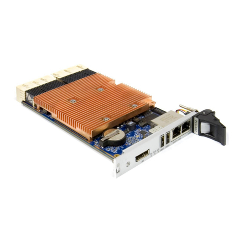
CPC505
C P C 5 0 5 U s e r M a n u a l 4 © 2 0 2 2 F a s t w e l v . 0 0 1
A8: RIO587 connectors………………………………………………………………………………………………….64
A9: Configuring and preparing the RIO587 module for operation………………………………………………….72
A10: RIO587 operating conditions and MTBF………………………………………………………………………….74
ANNEX B: MIC1901 mezzanine module…………………………….…………………………………………………………..75
B1: Introduction…………………………………………………………………………………………………………..75
B2: I/O Channel Structure of the MIC1901……………………………………………………………………………75
B3: Temperature range of the MIC1901………………………………………………………………………………75
B4: Appearance of the MIC1901 and layout of main elements……………………………………………………..76
B5: Information on MIC1901 packaging……………………………………………………………………………….79
B6: Delivery checklist of the MIC1901…………………………………………………………………………………79
B7: Specific performance features of the MIC1901 functional nodes……………………………………………...79
B8: Pinout charts of the MIC1901 connectors………………………………………………………………………..79
B9: Installation and preparation of the MIC1901 for operation……………………………………………………...80
B10: Operating Conditions of the MIC1901 and MTBF……………………………………………………………….83
ANNEX C: Terms and abbreviations ……………………………………………………………………………………….....84
ANNEX D: DISCLAIMER………………………………………………………………………………………………………….87
List of Tables
Table 2-1: Supply voltage of +5 V, +3.3 V from the CPCI bus..........................................................................14
Table 2-2: Maximum permissible consumption currents...................................................................................14
Table 2-3: Module versions ..............................................................................................................................15
Table 2-4: System information ……………………………………………………………..………………………….16
Table 3-1: Assignment of XMC XS4 (P15) connector pins ...……………………………………………………….22
Table 3-2: Assignment of XMC XS5 (P16) connector pins ……………………………………………………...….23
Table 3-3: Assignment of pins of the PMC XS2 (P1), XS3 (P3), XS6 (P2) and XS7 (P4) connectors ………...24
Table 3-4: Assignment of the M.2 XP5 connector pins ……………….…………………………………………….25
Table 3-5: Assignment of USB connectors pins on the front panel of the CPC505……..……………………….26
Table 3-6: Assignment of the Gigabit Ethernet connector pins …………………………………………………….27
Table 3-7: Assignment of the XS5 connector pins (DVI) of the CPC505 module …………………………….….28
Table 3-8: Assignment of the XS6 DisplayPort connector pins of the CPC505 module ………………………...29
Table 3-9: State of the SYS LED ………………………………...…………………………………………………....29
Table 3-10: Color code designations of connectors………….………………………………………………………..32
Table 3-11: Assignment of pins of the CompactPCI XS18 (J1) system connector …..……………………………32
Table 3-12: Assignment of the pins of XS16 (J2) system connector of 64-bit CompactPCI bus …..………….…33
Table 3-13: Assignment of XS11 (J3) connector pins of the CPC505…..…………………………………………..34
Table 3-14: Assignment of the XS8 (J4) connector pins of the CPC505……... ...………………………………....34
Table 3-15: Assignment of the XS1 (J5) connector pins of the CPC505……………………. ……………………..35
Table 3-16: Registers of SPI controller……………………………………. ……..……………………………………38
Table 3-17: Addresses of devices on SMBus ……………………………………………….…..………………….…40
Table 7-1: CPC505 fault causes and their troubleshooting ……………………………………………………..….50
Table 9-1: Processor frequency vs. temperature (for CPC505-01)……………………………………………...…52
Table 9-2: Environmental exposure when operating CPC505 ……………………………………………………..53
Table A-1: RIO587 versions ...………………………………..……………............................................................54
Table A-2: RIO587 temperature range (industrial and commercial version)………………………….…………..54
Table A-3: Weight of the RIO587-01 and RIO587-02 modules………………... ……..…………………………...55
Table A-4: Interfaces on rear panel of the RIO587-01 version…………...…………………..………………….…56
Table A-5: Additional interfaces on the rear panel of the RIO587-02 version ...………………………………….57
Table A-6: Additional interfaces at mezzanine connection …..………………. ...………………………………....59
Table A-7: Assignment of pins of the TH-4M connectors (XP3 and XP4) for feeding power to the CPC505....64
Table A-8: Assignment of pins of the PS/2 connector (XS4) for keyboard/mouse..……...………………………64
Table A-9: Assignment of the XP6 connector pins: COM1 port (RS232)………..…………..………………….…65
Table A-10: Assignment of pins of the XS11 connector: LPT port (IDC-26)….…………………………………….65
Table A-11: Assignment of pins of the XP10-XP12 connectors (COM2-COM4)………………………………...…66
Table A-12: Assignment of pins of the XP7 connector (COM5, RS485)………………………..…………………..66
Table A-13: Assignment of pins of the XP8 connector (COM6, RS485)…..………………………..……………....66
Table A-14: Assignment of the XP15 (SATA) connector pins ……..…………………………………….…………..67
Table A-15: Assignment of the ХS8 HDD …………………………….…………... ……..…………………………...67
Table A-16: Assignment of the CFast (XS5) card connector pins ….……..…………………..………………….…69
Table A-17: Assignment of the XP5 connector pins (GPIO and 3.3V power supply)………………………... ..….70
Table A-18: Assignment of the XP16 connector pins (LVDS) .…………………………………………..…………..71
Table A-19: Assignment of the XP19 connector pins (LCD panel backlight)………………………………….…....72
Table A-20: Power supply requirements for the RIO587…………………………………………..….….…………..73


